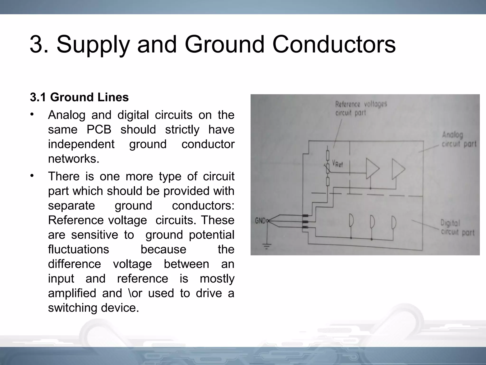
This document discusses design rules for analog circuit printed circuit boards (PCBs). It outlines three major factors: 1) component placing, 2) signal conductors, and 3) supply and ground conductors. For component placing, it recommends arranging components for access, adjustment, and heat dissipation. For signal conductors, it advises keeping lengths short to minimize interference and carefully laying out high frequency, feedback, and high gain circuits. For supply and ground conductors, it suggests keeping them independent for analog and digital circuits and reference voltages.
Single Stage Differential Folded Cascode AmplifierAalay Kapadia
The purpose of this project is to design a single-stage differential input and single-ended output) Amplifier. 0.35-um CMOS process and a supply voltage of 1.8 V is required in this design. The desired specifications is given. Among the single-stage topologies, the folded-cascade topology is chosen to meet the requirement for a high output swing design.
Introducing higher dielectric constant (k > 10) insulators [mainly transition metal (TM) oxides] is therefore indispensable for the 70 nm technology node and beyond
TM silicates such as HfSiOx have been preferred because they have better thermal stability compared to their oxides. The dielectric constant of TM silicates is less than TM oxides but higher than silicon oxide.
This presentation describes to you the very basic introduction of PN junction diode. All the topics and contents are presented in such a manner that students can understand it very easily and prepare it for final exam. At the end of this presentation, a few multiple choice questions (MCQ) are also there to test your knowledge on a particular topic that would be discussed in presentation.
GaN RF Market: Applications, Players, Technology and Substrates 2020Yole Developpement
Driven by military applications and 5G telecom infrastructure, the GaN RF market continues growing.
Learn more about the report here: https://www.i-micronews.com/products/gan-rf-market-applications-players-technology-and-substrates-2020/
The BGA category is set up to process area array devices
with interconnect spheres that are on common row and column pitches. It is optimized
for ease of programming and processing speed.
Threshold Voltage & Channel Length ModulationBulbul Brahma
Design and Technology of Electronic Devices:
Review of microelectronic devices, introduction to MOS technology and related devices.
MOS transistor theory, scaling theory related to MOS circuits, short channel effect and its
consequences, narrow width effect, FN tunnelling, Double gate MOSFET, Cylindrical
MOSFET, Basic concept of CMOS circuits and logic design. Circuit characterization and
performance estimation, important issues in real devices. PE logic, Domino logic, Pseudo
N-MOS logic-dynamic CMOS and Clocking, layout design and stick diagram, CMOS
analog circuit design, CMOS design methods. Introduction to SOI, Multi layer circuit
design and 3D integration. CMOS processing technology: Crystal grown and Epitaxy, Film
formation, Lithography and Etching, Impurity doping, Integrated Devices.
COMPLETE VIDEO IS AVAILABLE IN YOUTUBE
DOWNLOAD KICAD FROM https://kicad-pcb.org/
click here ----- https://www.youtube.com/channel/UCEMrYdeA40vFxjeNFjhEpRg?sub_confirmation=1
SUBSCRIBE TO THE CHANNEL
The performance obtainable from a single-stage amplifier is often insufficient for many applications, hence several stages may be combined forming a multistage amplifier. These stages are connected in cascade, i.e. output of the first stage is connected to form input of second stage, whose output becomes input of third stage, and so on.
thank u
Hansraj MEENA
Cmos fabrication is a part of semiconductor electronics that deals with the designing and fabrication process with NMOS and Cmos and other processes like Twin tub techniques and etc.
Phased Array Ultrasonic Testing (PAUT) is an advanced method of ultrasonic testing that has applications in medical imaging and industrial nondestructive testing. Common applications are to non-invasively examine the heart or to find flaws in manufactured materials such as welds.
Creative Hi-Tech would like to share some basics of Printed Circuit Boards which will help you to gain some knowledge before going to any vendor. This power point presentation will clear your basic doubts regarding the PCB.
Laser marking cell (I450) eliminates the doubt between a labelling or laser marking system!!
This option allows the machine to either directly mark the code on the solder resist, apply a label on which a code is marked or a mix of both. Please contact me through email: angela_kuo@126.com or angelaguo1688@gmail.com if you have interesting for this Laser Marking Machine.
We provide totally solution for LED lighting SMT PCB assembly.
Worldwide Installation and on site support.
Factory (machine and lighting assembly) training.
PCBA Assembly Process Flow / PCB Assembly Manufacturing introduces the basic manufacturing process of PCBA / PCB assembly in different condition of component.It is about PCBA manufacture production.
All the applications of ferrites is described in this presentation very briefly and presciously.
It would surely help you.
Please share it with your friends also.
a mosquito repellent circuit to generate a frequency range between 20-38 kHz. As this particular frequency is known as ultra sound it distracts the female mosquitoes .To make this circuit we are using here IC-555 timer, variable resistor, capacitor and to generate this ultrasound frequency we are using piezzo buzzer.
Sachpazis:Terzaghi Bearing Capacity Estimation in simple terms with Calculati...Dr.Costas Sachpazis
Terzaghi's soil bearing capacity theory, developed by Karl Terzaghi, is a fundamental principle in geotechnical engineering used to determine the bearing capacity of shallow foundations. This theory provides a method to calculate the ultimate bearing capacity of soil, which is the maximum load per unit area that the soil can support without undergoing shear failure. The Calculation HTML Code included.
Water scarcity is the lack of fresh water resources to meet the standard water demand. There are two type of water scarcity. One is physical. The other is economic water scarcity.
Student information management system project report ii.pdfKamal Acharya
Our project explains about the student management. This project mainly explains the various actions related to student details. This project shows some ease in adding, editing and deleting the student details. It also provides a less time consuming process for viewing, adding, editing and deleting the marks of the students.
Explore the innovative world of trenchless pipe repair with our comprehensive guide, "The Benefits and Techniques of Trenchless Pipe Repair." This document delves into the modern methods of repairing underground pipes without the need for extensive excavation, highlighting the numerous advantages and the latest techniques used in the industry.
Learn about the cost savings, reduced environmental impact, and minimal disruption associated with trenchless technology. Discover detailed explanations of popular techniques such as pipe bursting, cured-in-place pipe (CIPP) lining, and directional drilling. Understand how these methods can be applied to various types of infrastructure, from residential plumbing to large-scale municipal systems.
Ideal for homeowners, contractors, engineers, and anyone interested in modern plumbing solutions, this guide provides valuable insights into why trenchless pipe repair is becoming the preferred choice for pipe rehabilitation. Stay informed about the latest advancements and best practices in the field.
About
Indigenized remote control interface card suitable for MAFI system CCR equipment. Compatible for IDM8000 CCR. Backplane mounted serial and TCP/Ethernet communication module for CCR remote access. IDM 8000 CCR remote control on serial and TCP protocol.
• Remote control: Parallel or serial interface.
• Compatible with MAFI CCR system.
• Compatible with IDM8000 CCR.
• Compatible with Backplane mount serial communication.
• Compatible with commercial and Defence aviation CCR system.
• Remote control system for accessing CCR and allied system over serial or TCP.
• Indigenized local Support/presence in India.
• Easy in configuration using DIP switches.
Technical Specifications
Indigenized remote control interface card suitable for MAFI system CCR equipment. Compatible for IDM8000 CCR. Backplane mounted serial and TCP/Ethernet communication module for CCR remote access. IDM 8000 CCR remote control on serial and TCP protocol.
Key Features
Indigenized remote control interface card suitable for MAFI system CCR equipment. Compatible for IDM8000 CCR. Backplane mounted serial and TCP/Ethernet communication module for CCR remote access. IDM 8000 CCR remote control on serial and TCP protocol.
• Remote control: Parallel or serial interface
• Compatible with MAFI CCR system
• Copatiable with IDM8000 CCR
• Compatible with Backplane mount serial communication.
• Compatible with commercial and Defence aviation CCR system.
• Remote control system for accessing CCR and allied system over serial or TCP.
• Indigenized local Support/presence in India.
Application
• Remote control: Parallel or serial interface.
• Compatible with MAFI CCR system.
• Compatible with IDM8000 CCR.
• Compatible with Backplane mount serial communication.
• Compatible with commercial and Defence aviation CCR system.
• Remote control system for accessing CCR and allied system over serial or TCP.
• Indigenized local Support/presence in India.
• Easy in configuration using DIP switches.
CFD Simulation of By-pass Flow in a HRSG module by R&R Consult.pptxR&R Consult
CFD analysis is incredibly effective at solving mysteries and improving the performance of complex systems!
Here's a great example: At a large natural gas-fired power plant, where they use waste heat to generate steam and energy, they were puzzled that their boiler wasn't producing as much steam as expected.
R&R and Tetra Engineering Group Inc. were asked to solve the issue with reduced steam production.
An inspection had shown that a significant amount of hot flue gas was bypassing the boiler tubes, where the heat was supposed to be transferred.
R&R Consult conducted a CFD analysis, which revealed that 6.3% of the flue gas was bypassing the boiler tubes without transferring heat. The analysis also showed that the flue gas was instead being directed along the sides of the boiler and between the modules that were supposed to capture the heat. This was the cause of the reduced performance.
Based on our results, Tetra Engineering installed covering plates to reduce the bypass flow. This improved the boiler's performance and increased electricity production.
It is always satisfying when we can help solve complex challenges like this. Do your systems also need a check-up or optimization? Give us a call!
Work done in cooperation with James Malloy and David Moelling from Tetra Engineering.
More examples of our work https://www.r-r-consult.dk/en/cases-en/
NO1 Uk best vashikaran specialist in delhi vashikaran baba near me online vas...Amil Baba Dawood bangali
Contact with Dawood Bhai Just call on +92322-6382012 and we'll help you. We'll solve all your problems within 12 to 24 hours and with 101% guarantee and with astrology systematic. If you want to take any personal or professional advice then also you can call us on +92322-6382012 , ONLINE LOVE PROBLEM & Other all types of Daily Life Problem's.Then CALL or WHATSAPP us on +92322-6382012 and Get all these problems solutions here by Amil Baba DAWOOD BANGALI
#vashikaranspecialist #astrologer #palmistry #amliyaat #taweez #manpasandshadi #horoscope #spiritual #lovelife #lovespell #marriagespell#aamilbabainpakistan #amilbabainkarachi #powerfullblackmagicspell #kalajadumantarspecialist #realamilbaba #AmilbabainPakistan #astrologerincanada #astrologerindubai #lovespellsmaster #kalajaduspecialist #lovespellsthatwork #aamilbabainlahore#blackmagicformarriage #aamilbaba #kalajadu #kalailam #taweez #wazifaexpert #jadumantar #vashikaranspecialist #astrologer #palmistry #amliyaat #taweez #manpasandshadi #horoscope #spiritual #lovelife #lovespell #marriagespell#aamilbabainpakistan #amilbabainkarachi #powerfullblackmagicspell #kalajadumantarspecialist #realamilbaba #AmilbabainPakistan #astrologerincanada #astrologerindubai #lovespellsmaster #kalajaduspecialist #lovespellsthatwork #aamilbabainlahore #blackmagicforlove #blackmagicformarriage #aamilbaba #kalajadu #kalailam #taweez #wazifaexpert #jadumantar #vashikaranspecialist #astrologer #palmistry #amliyaat #taweez #manpasandshadi #horoscope #spiritual #lovelife #lovespell #marriagespell#aamilbabainpakistan #amilbabainkarachi #powerfullblackmagicspell #kalajadumantarspecialist #realamilbaba #AmilbabainPakistan #astrologerincanada #astrologerindubai #lovespellsmaster #kalajaduspecialist #lovespellsthatwork #aamilbabainlahore #Amilbabainuk #amilbabainspain #amilbabaindubai #Amilbabainnorway #amilbabainkrachi #amilbabainlahore #amilbabaingujranwalan #amilbabainislamabad
Hierarchical Digital Twin of a Naval Power SystemKerry Sado
A hierarchical digital twin of a Naval DC power system has been developed and experimentally verified. Similar to other state-of-the-art digital twins, this technology creates a digital replica of the physical system executed in real-time or faster, which can modify hardware controls. However, its advantage stems from distributing computational efforts by utilizing a hierarchical structure composed of lower-level digital twin blocks and a higher-level system digital twin. Each digital twin block is associated with a physical subsystem of the hardware and communicates with a singular system digital twin, which creates a system-level response. By extracting information from each level of the hierarchy, power system controls of the hardware were reconfigured autonomously. This hierarchical digital twin development offers several advantages over other digital twins, particularly in the field of naval power systems. The hierarchical structure allows for greater computational efficiency and scalability while the ability to autonomously reconfigure hardware controls offers increased flexibility and responsiveness. The hierarchical decomposition and models utilized were well aligned with the physical twin, as indicated by the maximum deviations between the developed digital twin hierarchy and the hardware.
Welcome to WIPAC Monthly the magazine brought to you by the LinkedIn Group Water Industry Process Automation & Control.
In this month's edition, along with this month's industry news to celebrate the 13 years since the group was created we have articles including
A case study of the used of Advanced Process Control at the Wastewater Treatment works at Lleida in Spain
A look back on an article on smart wastewater networks in order to see how the industry has measured up in the interim around the adoption of Digital Transformation in the Water Industry.
1. Design Rules For Analog Circuit PCB
Presented By:-
Shovana Khan Yusufzai
M.Tech in E.D&T
NIELIT, Gorakhpur
2. Major Factors in Designing Analog Circuit PCB
• 1 Component Placing
• 2 Signal Conductors
• 3 Supply and Ground Conductors
3. 1. Component Placing
• Components which need access from the front plate
have to be exactly according to the instructions of the
equipment designer.
• Components for internal adjustment such as,
potentiometer , trimmer, switches etc have to be
arranged near the board edge and oriented in the proper
direction.
• Component with metal case should not be placed very
near to the access path that is needed for adjustment of
screw driver other wise short circuit may occur.
4. • Heat producing components are regularly distributed
over the entire board area, as far as it is feasible. This is
to avoid a locally overheated board.
• Hot components have to be separated from the board
surface by suitable surfacers.
• The locating of heat sensitive components must avoid a
close proximity to hot components as well as a place in a
flow of already warmed up air.
5. 2. Signal Conductors
• Signal Conductors in analog circuit PCBs have to fulfill a
variety of different tasks, e.g. input, reference level,
feedback, output, etc.
• The length of any signal conductor should be made as
short as possible.This is because the magnitude of the
undesired inductive and capacitive coupling effects
increases more or less proportionally to the length of the
particular conductor.
• Apart from making of a good PCB, there are also other
techniques such as shielding or guarding with metallic
enclosures which have to be employed for a satisfactory
operation of equipment.
6. The signal conductor layout has to be done
particularly carefully for the following type of
circuits:
2.1 High Frequency Amplifiers/oscillators:
• At higher frequencies and with a long voltage supply line,
the circuit may oscillate because the voltage gain in an
emitter follower can be high i.e.,
Gain= Zcollector/Zemitter
• For precaution a capacitor is placed between the collector
and ground.
7. • And in case of oscillator similar problem occurs ,so to
avoid this, the layout has to be carefully made in order to
reduce the capacitive coupling.
8. • An improper layout of a high frequency
amplifier can also result in a reduced
bandwidth of the amplifier. If the input and
output conductors are close to each other ,
there can be a feedback resulting in
oscillations.
10. • If the ground and voltage conductors are long , a large
current I drawn by the high-power stage will flow through
the conductors with their own resistivity R.
• This additional resistance can modulate the Vcc and
GND of the input stage resulting in low frequency
oscillations which is called motorboating effect.
• To overcome this effect decoupling of the power supply
conductors with sufficiently large capacitor must be
done.
• Also separate Vcc and GND conductors can be provided
for two different stages.
11. 2.3 Feedback Amplifiers
• In designing high-wattage power supplies considerable
care in PCB layout design as well as in planning of the
remote sensing line to the front panel is necessary to
meet the regulation factor.
• A star grounding technique is used for the feedback
amplifier PCBs. The rectifier/capacitor circuit must be
connected to the star point for good cicuit performance.
12.
13. 2.4 High Gain DC Amplifiers(Thermal
Effects):
• When a device(transistor, DC amplifier) is soldered onto
the PCB, a thermocouple junction is formed between
copper( i.e. PCB conductor) and the kovar lead of the
transistor.
• If a temperature gradient exists, then different junctions
will create different voltages, thus effecting a noisy signal
to the amplifier.
14. 2.5 Amplifier handling low level signals
a) Low level, high impedance:
Due to high impedance the capacitive coupling occurs . For
reducing the coupling , it is necessary to provide
sufficient distance between the high impedance
conductors and other interfering signal lines.
b) Low level, low Impedance:
If the impedance is low one has to be careful about induced
voltage due to magnetic fields or inductive coupling.
15. 3. Supply and Ground Conductors
3.1 Ground Lines
• Analog and digital circuits on the
same PCB should strictly have
independent ground conductor
networks.
• There is one more type of circuit
part which should be provided with
separate ground conductors:
Reference voltage circuits. These
are sensitive to ground potential
fluctuations because the
difference voltage between an
input and reference is mostly
amplified and or used to drive a
switching device.
16. 3.2 Supply Lines
• Supply lines have to be provided with sufficient width to
keep resistance and inductivity low.
• Supply lines are connceted to the circuit end with the
highest signal power level.
• Reference voltage circuits should tap with the supply
lines directly at the input to the PCB.