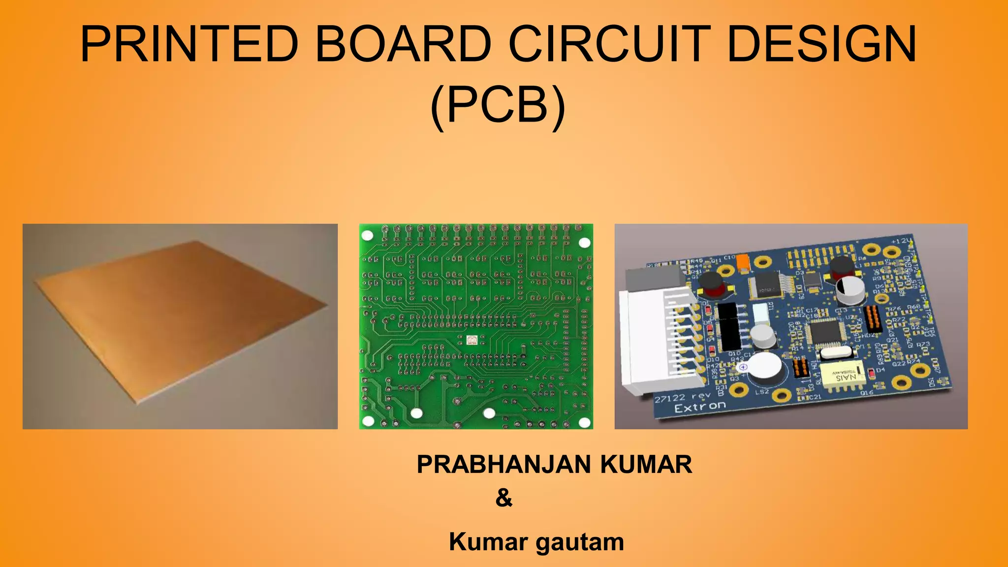
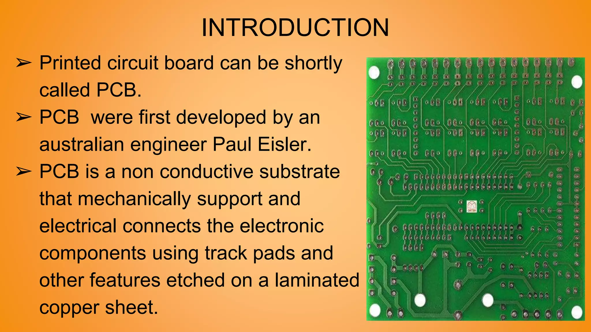
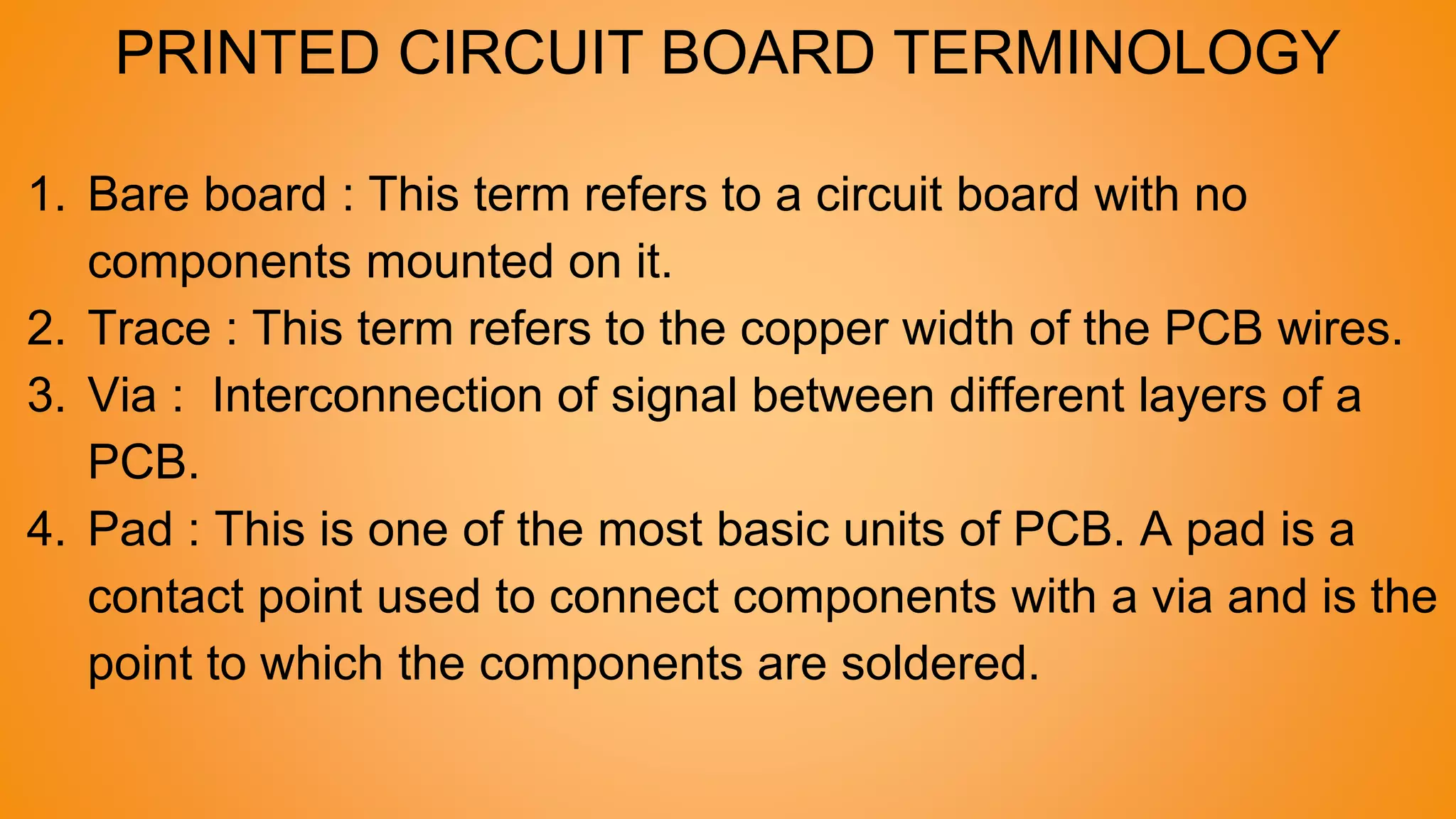
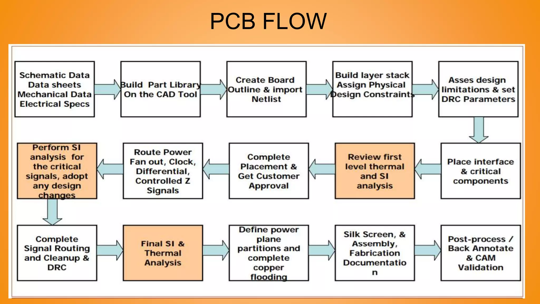
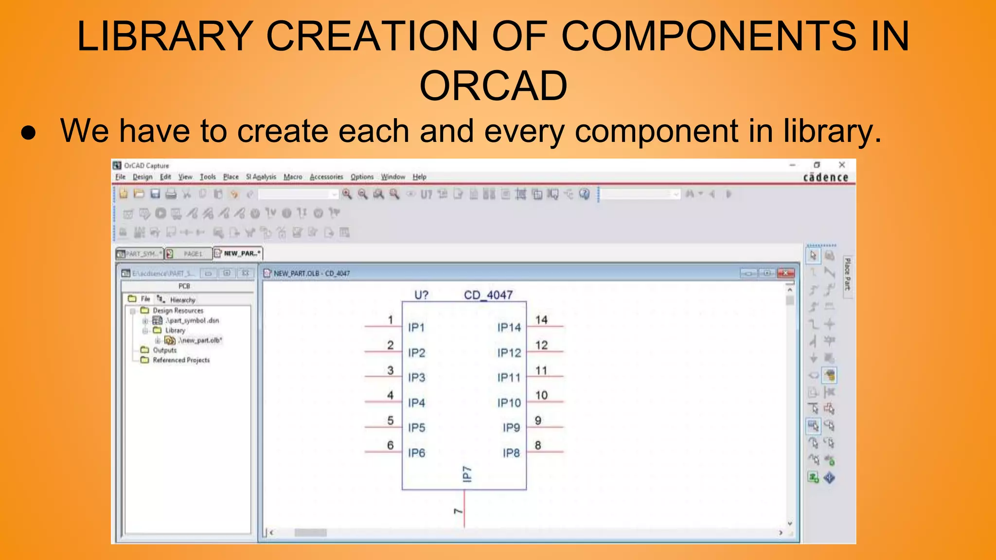
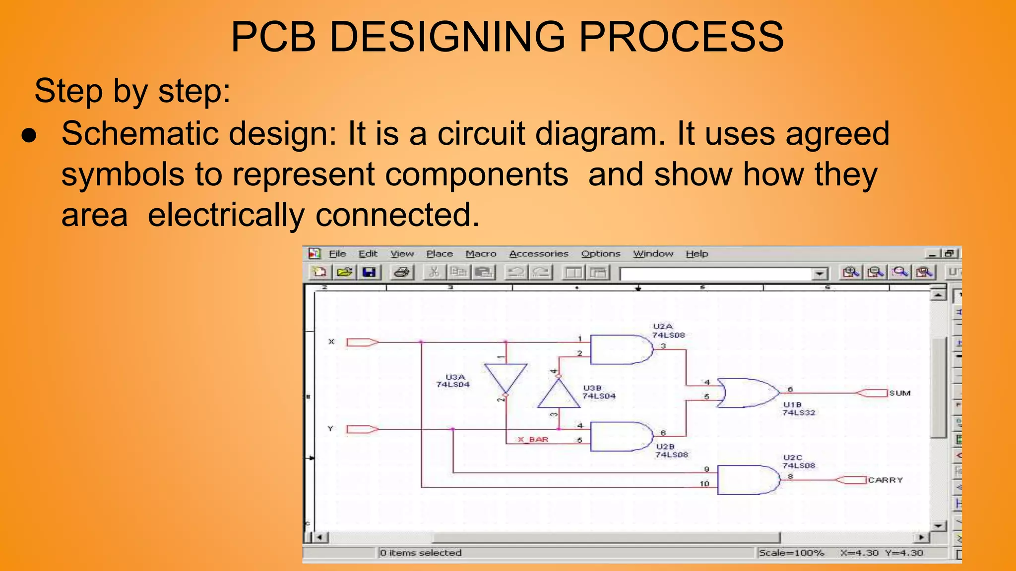
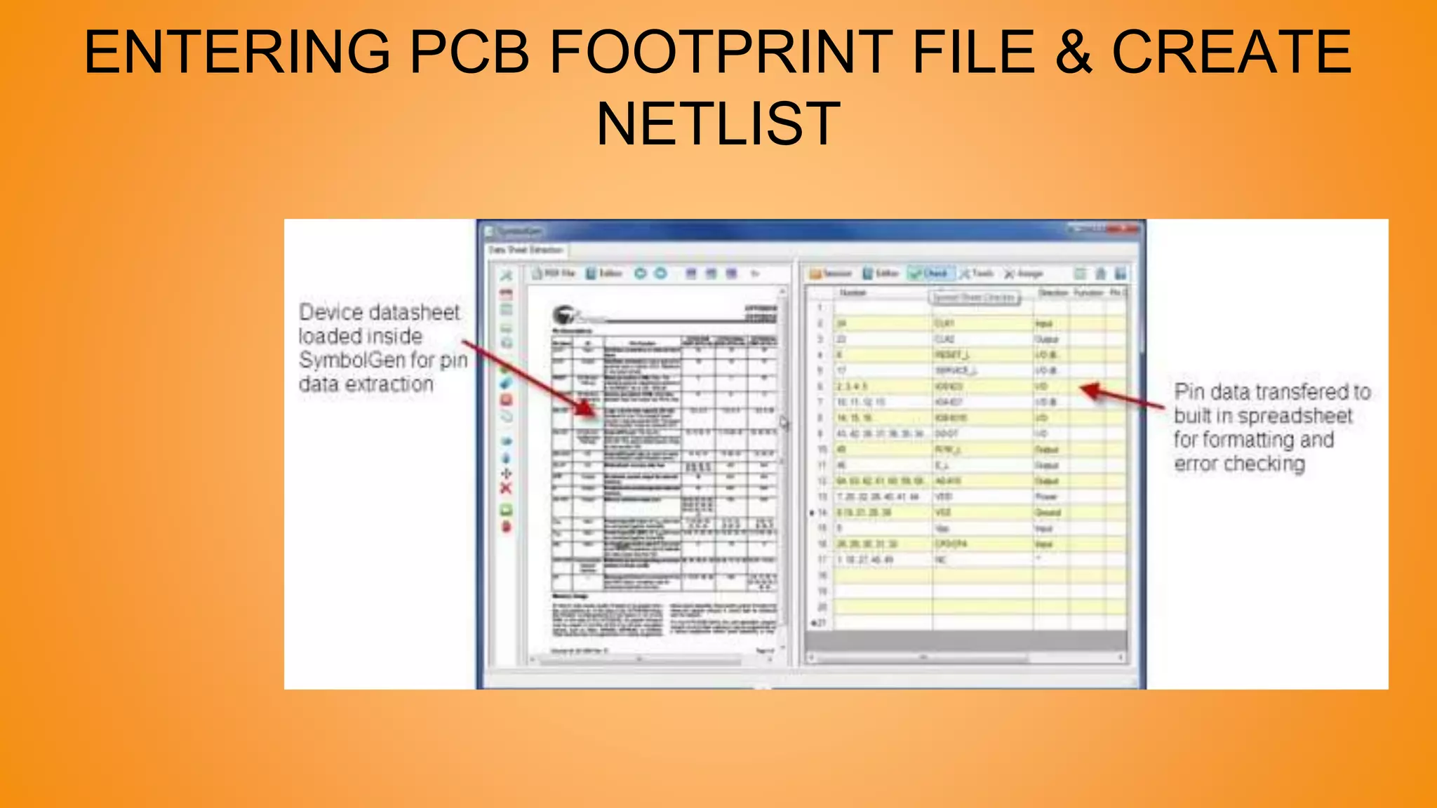
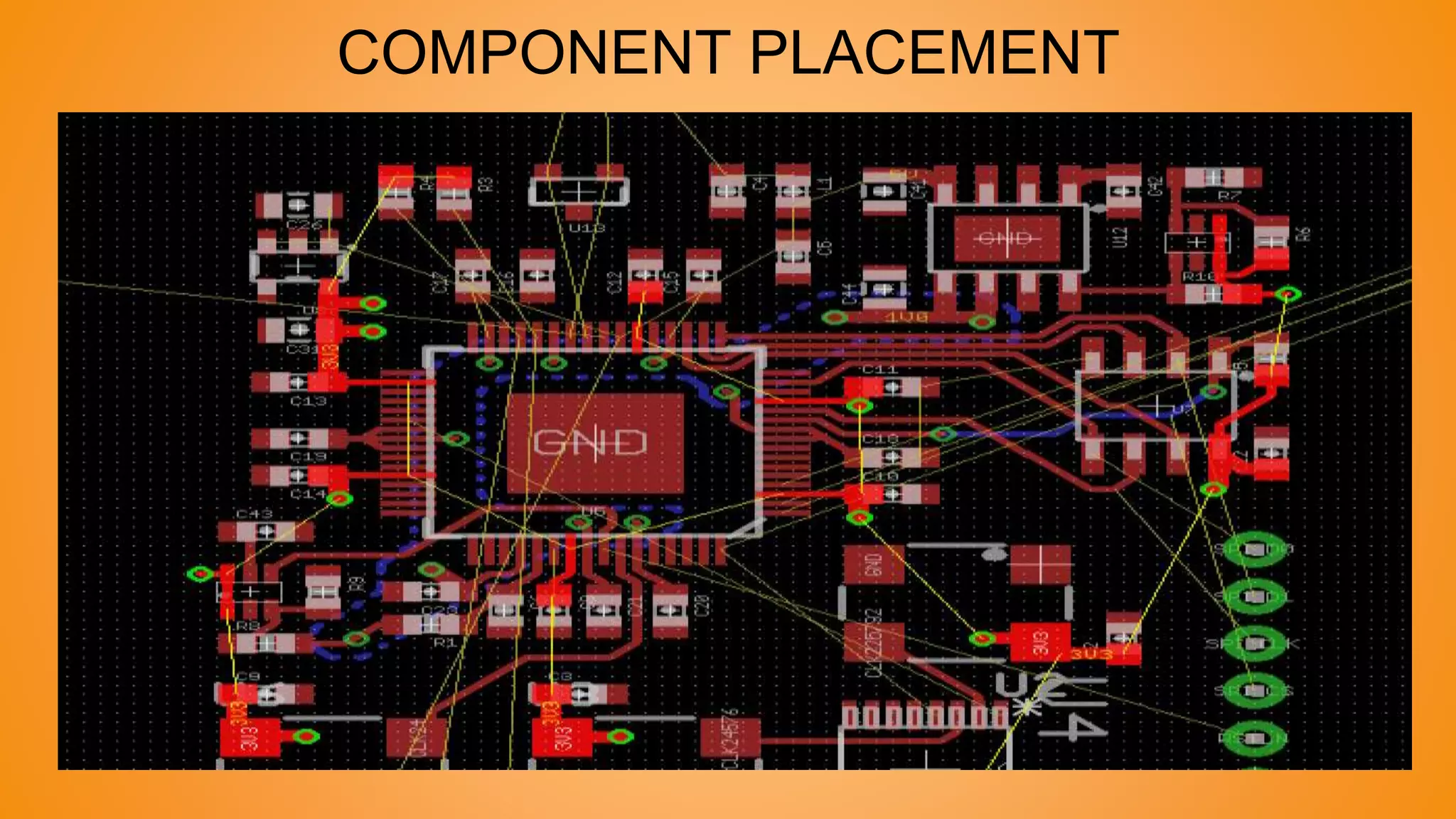
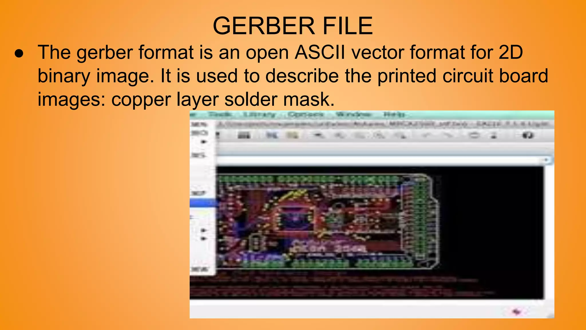
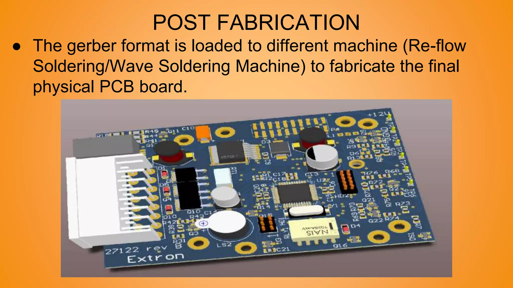
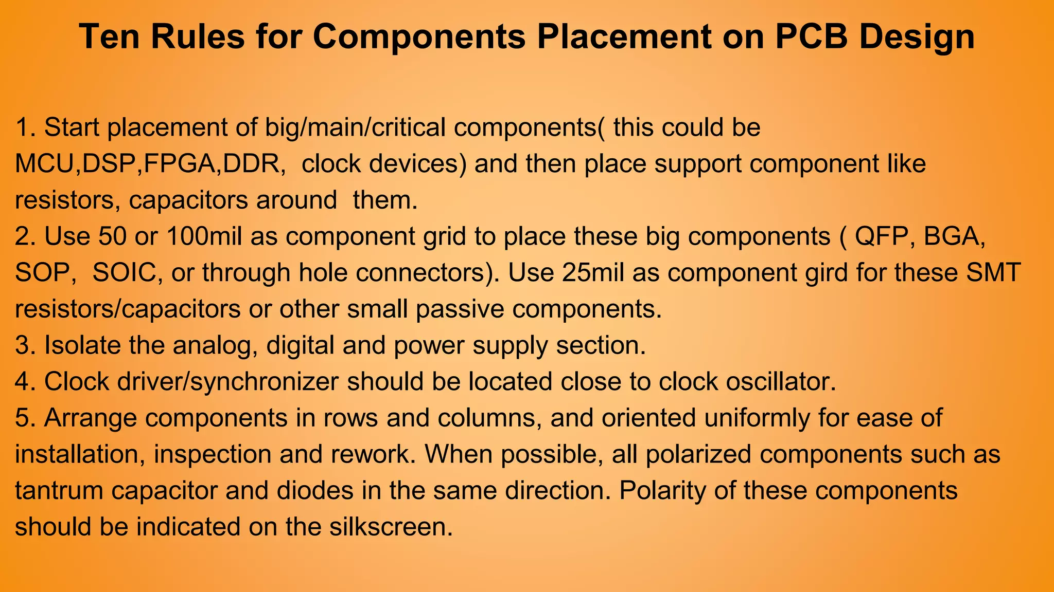
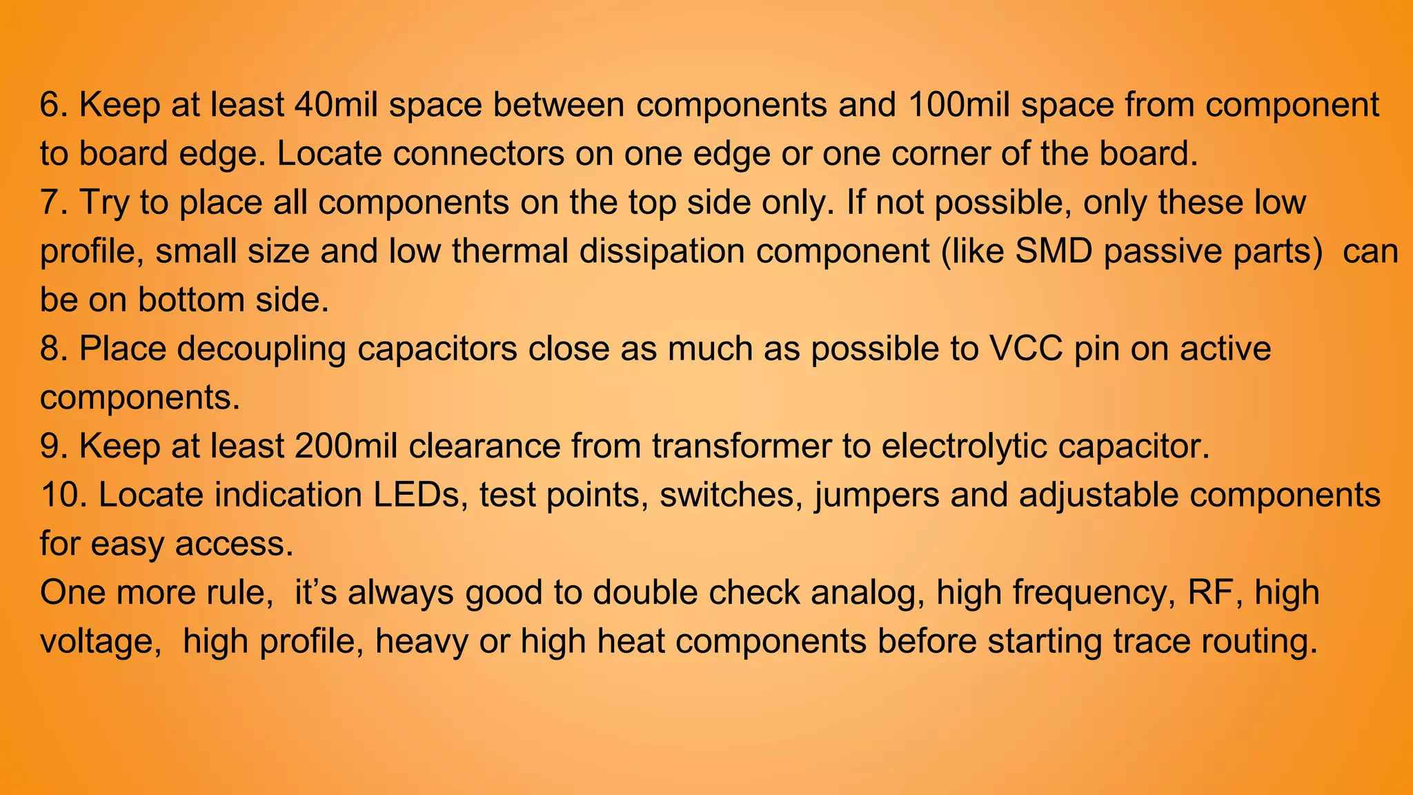
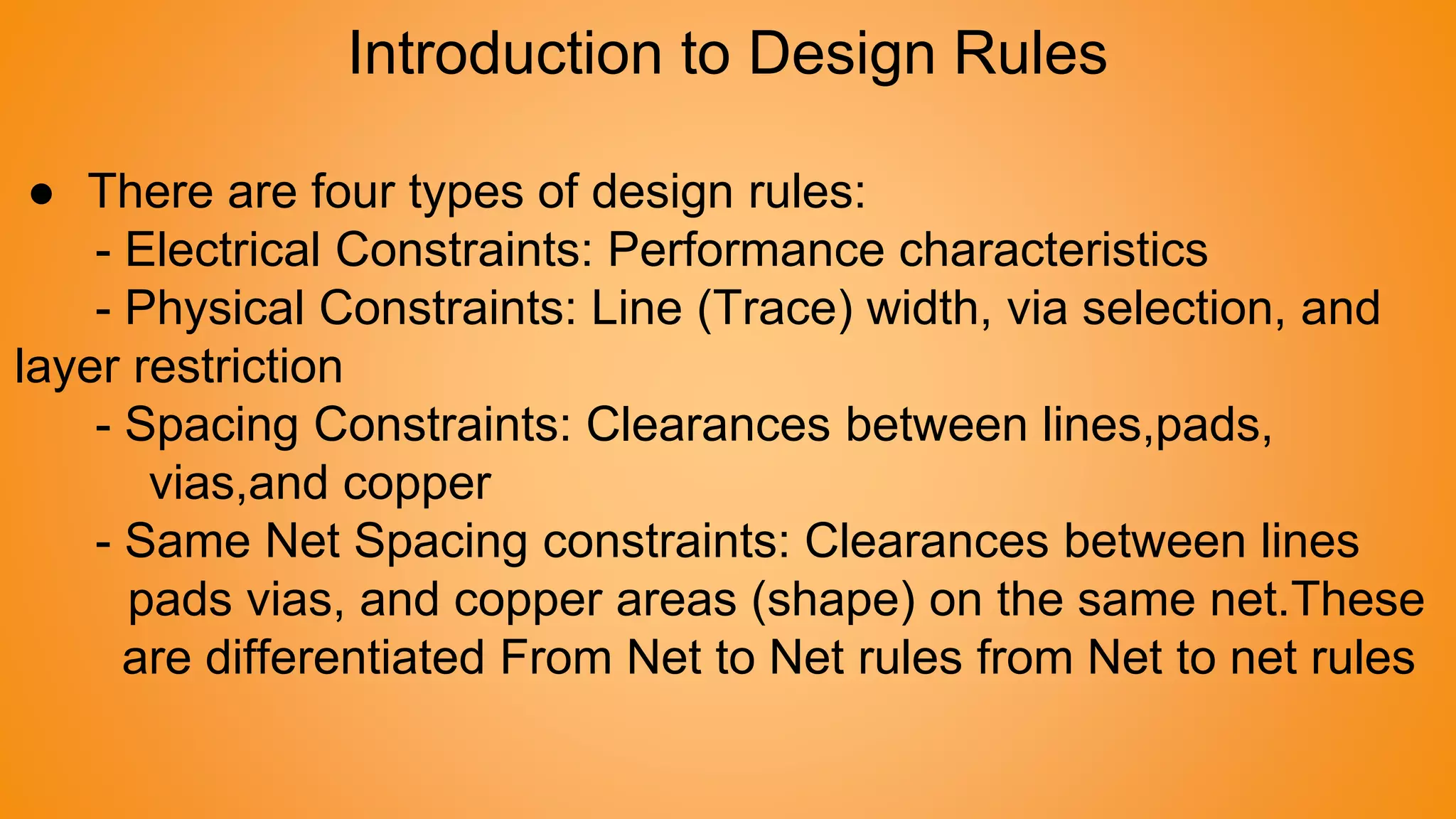
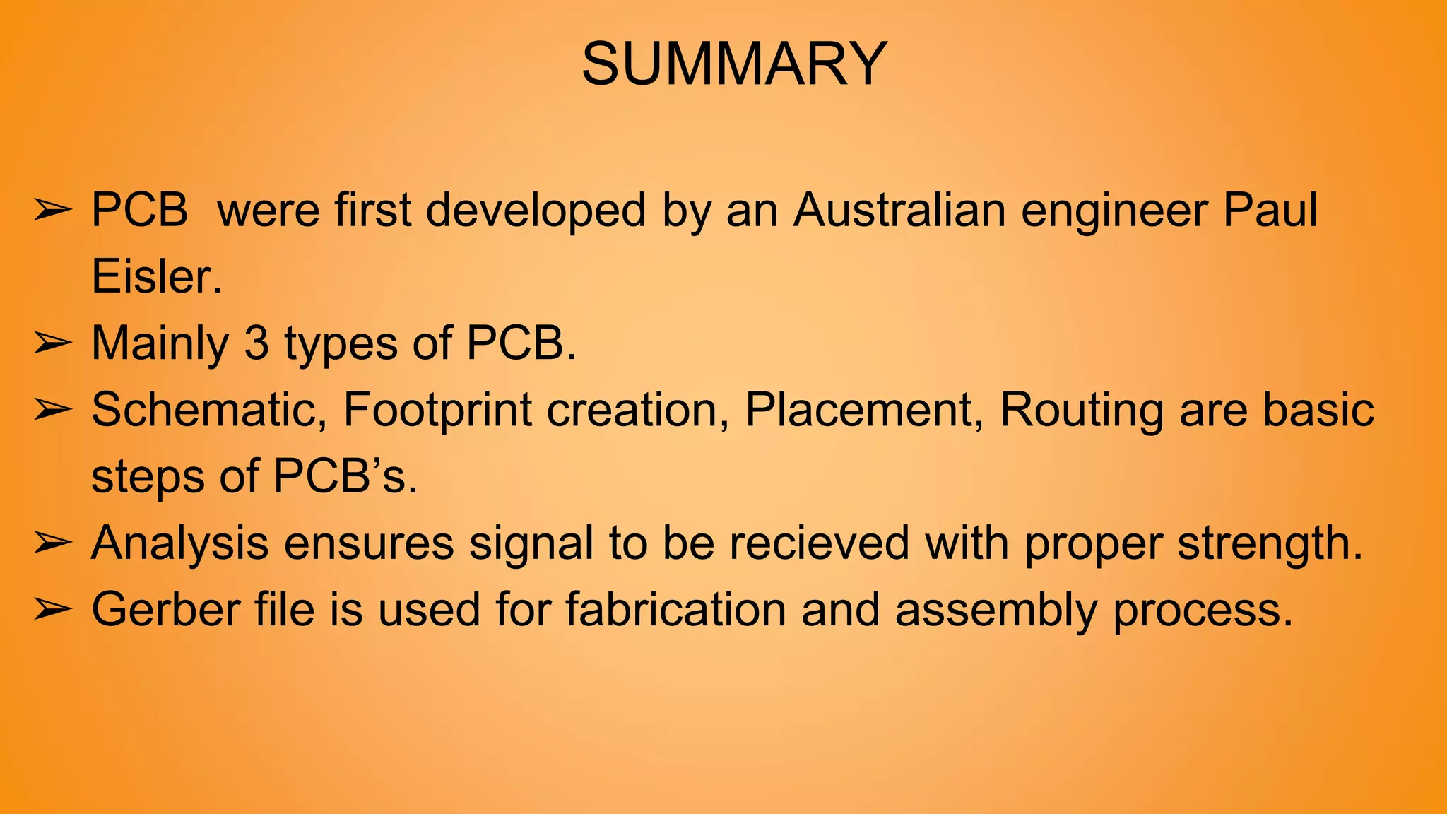
SlideShare a Scribd company logo
PRINTED BOARD CIRCUIT DESIGN
(PCB)
PRABHANJAN KUMAR
&
Kumar gautam
CONTENT
1. INTRODUCTION
2. TYPES OF PCB
3. PCB TERMINOLOGY
4. PCB FLOW
5. PLACEMENT RULES
6. INTRODUCTION TO DESIGN RULE
7. FABRICATED PCB BOARD
8. SUMMARY
INTRODUCTION
➢ Printed circuit board can be shortly
called PCB.
➢ PCB were first developed by an
australian engineer Paul Eisler.
➢ PCB is a non conductive substrate
that mechanically support and
electrical connects the electronic
components using track pads and
other features etched on a laminated
copper sheet.
TYPES OF PCB
There are mainly three types of PCBs
1. Single-sided PCB----- Component placement/Routing only on
one side (TOP/BOTTOM)
2. Double-sided PCB--- Component placement/Routing only on
both side (TOP & BOTTOM)
3. Multilayer PCB----Component placement on both side and
Routing also internal layers.
PRINTED CIRCUIT BOARD TERMINOLOGY
1. Bare board : This term refers to a circuit board with no
components mounted on it.
2. Trace : This term refers to the copper width of the PCB wires.
3. Via : Interconnection of signal between different layers of a
PCB.
4. Pad : This is one of the most basic units of PCB. A pad is a
contact point used to connect components with a via and is the
point to which the components are soldered.
PCB FLOW
LIBRARY CREATION OF COMPONENTS IN
ORCAD
● We have to create each and every component in library.
PCB DESIGNING PROCESS
Step by step:
● Schematic design: It is a circuit diagram. It uses agreed
symbols to represent components and show how they
area electrically connected.
ENTERING PCB FOOTPRINT FILE & CREATE
NETLIST
COMPONENT PLACEMENT
ROUTING & LENGTH MATCHING
● In electronic design, wire routing, commonly called
simply routing, is a step in the design of printed circuit
board and integrated circuit.
GERBER FILE
● The gerber format is an open ASCII vector format for 2D
binary image. It is used to describe the printed circuit board
images: copper layer solder mask.
POST FABRICATION
● The gerber format is loaded to different machine (Re-flow
Soldering/Wave Soldering Machine) to fabricate the final
physical PCB board.
Ten Rules for Components Placement on PCB Design
1. Start placement of big/main/critical components( this could be
MCU,DSP,FPGA,DDR, clock devices) and then place support component like
resistors, capacitors around them.
2. Use 50 or 100mil as component grid to place these big components ( QFP, BGA,
SOP, SOIC, or through hole connectors). Use 25mil as component gird for these SMT
resistors/capacitors or other small passive components.
3. Isolate the analog, digital and power supply section.
4. Clock driver/synchronizer should be located close to clock oscillator.
5. Arrange components in rows and columns, and oriented uniformly for ease of
installation, inspection and rework. When possible, all polarized components such as
tantrum capacitor and diodes in the same direction. Polarity of these components
should be indicated on the silkscreen.
6. Keep at least 40mil space between components and 100mil space from component
to board edge. Locate connectors on one edge or one corner of the board.
7. Try to place all components on the top side only. If not possible, only these low
profile, small size and low thermal dissipation component (like SMD passive parts) can
be on bottom side.
8. Place decoupling capacitors close as much as possible to VCC pin on active
components.
9. Keep at least 200mil clearance from transformer to electrolytic capacitor.
10. Locate indication LEDs, test points, switches, jumpers and adjustable components
for easy access.
One more rule, it’s always good to double check analog, high frequency, RF, high
voltage, high profile, heavy or high heat components before starting trace routing.
Introduction to Design Rules
● There are four types of design rules:
- Electrical Constraints: Performance characteristics
- Physical Constraints: Line (Trace) width, via selection, and
layer restriction
- Spacing Constraints: Clearances between lines,pads,
vias,and copper
- Same Net Spacing constraints: Clearances between lines
pads vias, and copper areas (shape) on the same net.These
are differentiated From Net to Net rules from Net to net rules
SUMMARY
➢ PCB were first developed by an Australian engineer Paul
Eisler.
➢ Mainly 3 types of PCB.
➢ Schematic, Footprint creation, Placement, Routing are basic
steps of PCB’s.
➢ Analysis ensures signal to be recieved with proper strength.
➢ Gerber file is used for fabrication and assembly process.
QUESTIONS???
Thank you

More Related Content

What's hot

pcb
pcbpcb
Types of PCB Designing Layers
Types of PCB Designing LayersTypes of PCB Designing Layers
Types of PCB Designing Layers
Sharan kumar
 
Introduction to PCB Design
Introduction to PCB DesignIntroduction to PCB Design
Introduction to PCB DesignSharan kumar
 
Pcb design powerpoint
Pcb design powerpointPcb design powerpoint
Pcb design powerpoint
Prashant329822
 
SURFACE MOUNT TECHNOLOGY
SURFACE MOUNT TECHNOLOGYSURFACE MOUNT TECHNOLOGY
SURFACE MOUNT TECHNOLOGYSubhendra Singh
 
Printed circuit Board Description
Printed circuit Board DescriptionPrinted circuit Board Description
Printed circuit Board DescriptionRUBY DIKSHIT
 
Introduction to Surface Mount Technology
Introduction to Surface Mount TechnologyIntroduction to Surface Mount Technology
Introduction to Surface Mount Technology
ABDUL MUNAFF
 
PCB Designing
PCB Designing PCB Designing
PCB Designing
kaleem Ullah
 
Fabrication steps of IC
Fabrication steps of ICFabrication steps of IC
Fabrication steps of IC
Gowri Kishore
 
Introduction to PCB Designing
Introduction to PCB DesigningIntroduction to PCB Designing
Introduction to PCB Designing
Sharan kumar
 
Surface mount technology(smt)
Surface mount technology(smt)Surface mount technology(smt)
Surface mount technology(smt)
AshutoshKumar1262
 
Introduction to active and passive components
Introduction to active and passive components Introduction to active and passive components
Introduction to active and passive components
DeependraGoswami
 
Printed circuit board
Printed circuit boardPrinted circuit board
Printed circuit board
Suhail Ahmed
 
Electronic components
Electronic componentsElectronic components
Electronic components
Unsa Shakir
 
PPT ON PCB DESIGN INTERNSHIP
PPT ON PCB DESIGN INTERNSHIPPPT ON PCB DESIGN INTERNSHIP
PPT ON PCB DESIGN INTERNSHIP
SujoyHalder4
 
Introduction to PCB Design (Eagle)
Introduction to PCB Design (Eagle)Introduction to PCB Design (Eagle)
Introduction to PCB Design (Eagle)
yeokm1
 

What's hot (20)

pcb
pcbpcb
pcb
 
Types of PCB Designing Layers
Types of PCB Designing LayersTypes of PCB Designing Layers
Types of PCB Designing Layers
 
Introduction to PCB Design
Introduction to PCB DesignIntroduction to PCB Design
Introduction to PCB Design
 
WelcomePCB
WelcomePCBWelcomePCB
WelcomePCB
 
Pcb design powerpoint
Pcb design powerpointPcb design powerpoint
Pcb design powerpoint
 
INTRODUCTION TO PCB
INTRODUCTION TO PCBINTRODUCTION TO PCB
INTRODUCTION TO PCB
 
SURFACE MOUNT TECHNOLOGY
SURFACE MOUNT TECHNOLOGYSURFACE MOUNT TECHNOLOGY
SURFACE MOUNT TECHNOLOGY
 
Printed circuit Board Description
Printed circuit Board DescriptionPrinted circuit Board Description
Printed circuit Board Description
 
Introduction to Surface Mount Technology
Introduction to Surface Mount TechnologyIntroduction to Surface Mount Technology
Introduction to Surface Mount Technology
 
PCB Designing
PCB Designing PCB Designing
PCB Designing
 
Fabrication steps of IC
Fabrication steps of ICFabrication steps of IC
Fabrication steps of IC
 
Introduction to PCB Designing
Introduction to PCB DesigningIntroduction to PCB Designing
Introduction to PCB Designing
 
Surface mount technology(smt)
Surface mount technology(smt)Surface mount technology(smt)
Surface mount technology(smt)
 
Introduction to active and passive components
Introduction to active and passive components Introduction to active and passive components
Introduction to active and passive components
 
PCB
PCB PCB
PCB
 
Printed circuit board
Printed circuit boardPrinted circuit board
Printed circuit board
 
Electronic components
Electronic componentsElectronic components
Electronic components
 
PPT ON PCB DESIGN INTERNSHIP
PPT ON PCB DESIGN INTERNSHIPPPT ON PCB DESIGN INTERNSHIP
PPT ON PCB DESIGN INTERNSHIP
 
Introduction to PCB Design (Eagle)
Introduction to PCB Design (Eagle)Introduction to PCB Design (Eagle)
Introduction to PCB Design (Eagle)
 
PCB
PCBPCB
PCB
 

Similar to Printed board circuit design (Pcb) PPT

Design of Printed Circuit Boards
Design of Printed Circuit BoardsDesign of Printed Circuit Boards
Design of Printed Circuit Boards
Chandana129742
 
Pcb design using_eagle
Pcb design using_eaglePcb design using_eagle
Pcb design using_eagle
ABDUL MUNAFF
 
PCB fabrication.pptx
PCB fabrication.pptxPCB fabrication.pptx
PCB fabrication.pptx
RavinaBishnoi8
 
Electronic circuit design and component selection.pptx
Electronic circuit design and component selection.pptxElectronic circuit design and component selection.pptx
Electronic circuit design and component selection.pptx
maheshmp16
 
ACHAL NEET PPT OF PCB-1.pptx
ACHAL NEET PPT OF PCB-1.pptxACHAL NEET PPT OF PCB-1.pptx
ACHAL NEET PPT OF PCB-1.pptx
Tusharchauhan939328
 
Pcb layout
Pcb layoutPcb layout
Pcb layout
panchal_jay
 
Surface mount technology (smt) and smd packages
Surface mount technology (smt) and smd packagesSurface mount technology (smt) and smd packages
Surface mount technology (smt) and smd packages
karen zou
 
PCB
PCBPCB
PCB desine final.pdf
PCB desine final.pdfPCB desine final.pdf
PCB desine final.pdf
Tusharchauhan939328
 
Pcbdesign 140510145153-phpapp01
Pcbdesign 140510145153-phpapp01Pcbdesign 140510145153-phpapp01
Pcbdesign 140510145153-phpapp01
ssantosh1234
 
Pcb design
Pcb designPcb design
Pcb design
Abu Bakker
 
Pcb design
Pcb designPcb design
Pcb design
Abu Bakker
 
PCB Terminologies in PCB designing
PCB Terminologies in PCB designingPCB Terminologies in PCB designing
PCB Terminologies in PCB designing
MSHOAIBASLAM1
 
PCB Fabrication, China PCB Circuit Board Manufacturing from China
PCB Fabrication, China PCB Circuit Board Manufacturing from ChinaPCB Fabrication, China PCB Circuit Board Manufacturing from China
PCB Fabrication, China PCB Circuit Board Manufacturing from China
Leah-Hitech PCB
 
PCB Assembly Manufacturer Hitech circuits
PCB Assembly Manufacturer Hitech circuitsPCB Assembly Manufacturer Hitech circuits
PCB Assembly Manufacturer Hitech circuits
Karen--PCBA Manufacturer--Hitech Circuits
 
Learning outcome 2 prepare make pcb modules
Learning outcome 2 prepare make pcb modulesLearning outcome 2 prepare make pcb modules
Learning outcome 2 prepare make pcb modules
Ar Kyu Dee
 
Importance of PCB assembly in Various Industries | Suntronic Inc |
Importance of PCB assembly in Various Industries | Suntronic Inc |Importance of PCB assembly in Various Industries | Suntronic Inc |
Importance of PCB assembly in Various Industries | Suntronic Inc |
SuntronicInc
 
Chapter12 manufacturing-processes
Chapter12 manufacturing-processesChapter12 manufacturing-processes
Chapter12 manufacturing-processesVin Voro
 
presentation1-131031235854-phpapp02.pptx
presentation1-131031235854-phpapp02.pptxpresentation1-131031235854-phpapp02.pptx
presentation1-131031235854-phpapp02.pptx
SirachartChuto
 
Printed Circuit Board Design Techniques for EMC Compliance_20240220_145105_00...
Printed Circuit Board Design Techniques for EMC Compliance_20240220_145105_00...Printed Circuit Board Design Techniques for EMC Compliance_20240220_145105_00...
Printed Circuit Board Design Techniques for EMC Compliance_20240220_145105_00...
AlanGustavo13
 

Similar to Printed board circuit design (Pcb) PPT (20)

Design of Printed Circuit Boards
Design of Printed Circuit BoardsDesign of Printed Circuit Boards
Design of Printed Circuit Boards
 
Pcb design using_eagle
Pcb design using_eaglePcb design using_eagle
Pcb design using_eagle
 
PCB fabrication.pptx
PCB fabrication.pptxPCB fabrication.pptx
PCB fabrication.pptx
 
Electronic circuit design and component selection.pptx
Electronic circuit design and component selection.pptxElectronic circuit design and component selection.pptx
Electronic circuit design and component selection.pptx
 
ACHAL NEET PPT OF PCB-1.pptx
ACHAL NEET PPT OF PCB-1.pptxACHAL NEET PPT OF PCB-1.pptx
ACHAL NEET PPT OF PCB-1.pptx
 
Pcb layout
Pcb layoutPcb layout
Pcb layout
 
Surface mount technology (smt) and smd packages
Surface mount technology (smt) and smd packagesSurface mount technology (smt) and smd packages
Surface mount technology (smt) and smd packages
 
PCB
PCBPCB
PCB
 
PCB desine final.pdf
PCB desine final.pdfPCB desine final.pdf
PCB desine final.pdf
 
Pcbdesign 140510145153-phpapp01
Pcbdesign 140510145153-phpapp01Pcbdesign 140510145153-phpapp01
Pcbdesign 140510145153-phpapp01
 
Pcb design
Pcb designPcb design
Pcb design
 
Pcb design
Pcb designPcb design
Pcb design
 
PCB Terminologies in PCB designing
PCB Terminologies in PCB designingPCB Terminologies in PCB designing
PCB Terminologies in PCB designing
 
PCB Fabrication, China PCB Circuit Board Manufacturing from China
PCB Fabrication, China PCB Circuit Board Manufacturing from ChinaPCB Fabrication, China PCB Circuit Board Manufacturing from China
PCB Fabrication, China PCB Circuit Board Manufacturing from China
 
PCB Assembly Manufacturer Hitech circuits
PCB Assembly Manufacturer Hitech circuitsPCB Assembly Manufacturer Hitech circuits
PCB Assembly Manufacturer Hitech circuits
 
Learning outcome 2 prepare make pcb modules
Learning outcome 2 prepare make pcb modulesLearning outcome 2 prepare make pcb modules
Learning outcome 2 prepare make pcb modules
 
Importance of PCB assembly in Various Industries | Suntronic Inc |
Importance of PCB assembly in Various Industries | Suntronic Inc |Importance of PCB assembly in Various Industries | Suntronic Inc |
Importance of PCB assembly in Various Industries | Suntronic Inc |
 
Chapter12 manufacturing-processes
Chapter12 manufacturing-processesChapter12 manufacturing-processes
Chapter12 manufacturing-processes
 
presentation1-131031235854-phpapp02.pptx
presentation1-131031235854-phpapp02.pptxpresentation1-131031235854-phpapp02.pptx
presentation1-131031235854-phpapp02.pptx
 
Printed Circuit Board Design Techniques for EMC Compliance_20240220_145105_00...
Printed Circuit Board Design Techniques for EMC Compliance_20240220_145105_00...Printed Circuit Board Design Techniques for EMC Compliance_20240220_145105_00...
Printed Circuit Board Design Techniques for EMC Compliance_20240220_145105_00...
 

Recently uploaded

ethical hacking in wireless-hacking1.ppt
ethical hacking in wireless-hacking1.pptethical hacking in wireless-hacking1.ppt
ethical hacking in wireless-hacking1.ppt
Jayaprasanna4
 
WATER CRISIS and its solutions-pptx 1234
WATER CRISIS and its solutions-pptx 1234WATER CRISIS and its solutions-pptx 1234
WATER CRISIS and its solutions-pptx 1234
AafreenAbuthahir2
 
The role of big data in decision making.
The role of big data in decision making.The role of big data in decision making.
The role of big data in decision making.
ankuprajapati0525
 
Runway Orientation Based on the Wind Rose Diagram.pptx
Runway Orientation Based on the Wind Rose Diagram.pptxRunway Orientation Based on the Wind Rose Diagram.pptx
Runway Orientation Based on the Wind Rose Diagram.pptx
SupreethSP4
 
Top 10 Oil and Gas Projects in Saudi Arabia 2024.pdf
Top 10 Oil and Gas Projects in Saudi Arabia 2024.pdfTop 10 Oil and Gas Projects in Saudi Arabia 2024.pdf
Top 10 Oil and Gas Projects in Saudi Arabia 2024.pdf
Teleport Manpower Consultant
 
CFD Simulation of By-pass Flow in a HRSG module by R&R Consult.pptx
CFD Simulation of By-pass Flow in a HRSG module by R&R Consult.pptxCFD Simulation of By-pass Flow in a HRSG module by R&R Consult.pptx
CFD Simulation of By-pass Flow in a HRSG module by R&R Consult.pptx
R&R Consult
 
Immunizing Image Classifiers Against Localized Adversary Attacks
Immunizing Image Classifiers Against Localized Adversary AttacksImmunizing Image Classifiers Against Localized Adversary Attacks
Immunizing Image Classifiers Against Localized Adversary Attacks
gerogepatton
 
RAT: Retrieval Augmented Thoughts Elicit Context-Aware Reasoning in Long-Hori...
RAT: Retrieval Augmented Thoughts Elicit Context-Aware Reasoning in Long-Hori...RAT: Retrieval Augmented Thoughts Elicit Context-Aware Reasoning in Long-Hori...
RAT: Retrieval Augmented Thoughts Elicit Context-Aware Reasoning in Long-Hori...
thanhdowork
 
weather web application report.pdf
weather web application report.pdfweather web application report.pdf
weather web application report.pdf
Pratik Pawar
 
Architectural Portfolio Sean Lockwood
Architectural Portfolio Sean LockwoodArchitectural Portfolio Sean Lockwood
Architectural Portfolio Sean Lockwood
seandesed
 
ethical hacking-mobile hacking methods.ppt
ethical hacking-mobile hacking methods.pptethical hacking-mobile hacking methods.ppt
ethical hacking-mobile hacking methods.ppt
Jayaprasanna4
 
NO1 Uk best vashikaran specialist in delhi vashikaran baba near me online vas...
NO1 Uk best vashikaran specialist in delhi vashikaran baba near me online vas...NO1 Uk best vashikaran specialist in delhi vashikaran baba near me online vas...
NO1 Uk best vashikaran specialist in delhi vashikaran baba near me online vas...
Amil Baba Dawood bangali
 
J.Yang, ICLR 2024, MLILAB, KAIST AI.pdf
J.Yang,  ICLR 2024, MLILAB, KAIST AI.pdfJ.Yang,  ICLR 2024, MLILAB, KAIST AI.pdf
J.Yang, ICLR 2024, MLILAB, KAIST AI.pdf
MLILAB
 
Pile Foundation by Venkatesh Taduvai (Sub Geotechnical Engineering II)-conver...
Pile Foundation by Venkatesh Taduvai (Sub Geotechnical Engineering II)-conver...Pile Foundation by Venkatesh Taduvai (Sub Geotechnical Engineering II)-conver...
Pile Foundation by Venkatesh Taduvai (Sub Geotechnical Engineering II)-conver...
AJAYKUMARPUND1
 
Student information management system project report ii.pdf
Student information management system project report ii.pdfStudent information management system project report ii.pdf
Student information management system project report ii.pdf
Kamal Acharya
 
Final project report on grocery store management system..pdf
Final project report on grocery store management system..pdfFinal project report on grocery store management system..pdf
Final project report on grocery store management system..pdf
Kamal Acharya
 
MCQ Soil mechanics questions (Soil shear strength).pdf
MCQ Soil mechanics questions (Soil shear strength).pdfMCQ Soil mechanics questions (Soil shear strength).pdf
MCQ Soil mechanics questions (Soil shear strength).pdf
Osamah Alsalih
 
power quality voltage fluctuation UNIT - I.pptx
power quality voltage fluctuation UNIT - I.pptxpower quality voltage fluctuation UNIT - I.pptx
power quality voltage fluctuation UNIT - I.pptx
ViniHema
 
一比一原版(SFU毕业证)西蒙菲莎大学毕业证成绩单如何办理
一比一原版(SFU毕业证)西蒙菲莎大学毕业证成绩单如何办理一比一原版(SFU毕业证)西蒙菲莎大学毕业证成绩单如何办理
一比一原版(SFU毕业证)西蒙菲莎大学毕业证成绩单如何办理
bakpo1
 
AKS UNIVERSITY Satna Final Year Project By OM Hardaha.pdf
AKS UNIVERSITY Satna Final Year Project By OM Hardaha.pdfAKS UNIVERSITY Satna Final Year Project By OM Hardaha.pdf
AKS UNIVERSITY Satna Final Year Project By OM Hardaha.pdf
SamSarthak3
 

Recently uploaded (20)

ethical hacking in wireless-hacking1.ppt
ethical hacking in wireless-hacking1.pptethical hacking in wireless-hacking1.ppt
ethical hacking in wireless-hacking1.ppt
 
WATER CRISIS and its solutions-pptx 1234
WATER CRISIS and its solutions-pptx 1234WATER CRISIS and its solutions-pptx 1234
WATER CRISIS and its solutions-pptx 1234
 
The role of big data in decision making.
The role of big data in decision making.The role of big data in decision making.
The role of big data in decision making.
 
Runway Orientation Based on the Wind Rose Diagram.pptx
Runway Orientation Based on the Wind Rose Diagram.pptxRunway Orientation Based on the Wind Rose Diagram.pptx
Runway Orientation Based on the Wind Rose Diagram.pptx
 
Top 10 Oil and Gas Projects in Saudi Arabia 2024.pdf
Top 10 Oil and Gas Projects in Saudi Arabia 2024.pdfTop 10 Oil and Gas Projects in Saudi Arabia 2024.pdf
Top 10 Oil and Gas Projects in Saudi Arabia 2024.pdf
 
CFD Simulation of By-pass Flow in a HRSG module by R&R Consult.pptx
CFD Simulation of By-pass Flow in a HRSG module by R&R Consult.pptxCFD Simulation of By-pass Flow in a HRSG module by R&R Consult.pptx
CFD Simulation of By-pass Flow in a HRSG module by R&R Consult.pptx
 
Immunizing Image Classifiers Against Localized Adversary Attacks
Immunizing Image Classifiers Against Localized Adversary AttacksImmunizing Image Classifiers Against Localized Adversary Attacks
Immunizing Image Classifiers Against Localized Adversary Attacks
 
RAT: Retrieval Augmented Thoughts Elicit Context-Aware Reasoning in Long-Hori...
RAT: Retrieval Augmented Thoughts Elicit Context-Aware Reasoning in Long-Hori...RAT: Retrieval Augmented Thoughts Elicit Context-Aware Reasoning in Long-Hori...
RAT: Retrieval Augmented Thoughts Elicit Context-Aware Reasoning in Long-Hori...
 
weather web application report.pdf
weather web application report.pdfweather web application report.pdf
weather web application report.pdf
 
Architectural Portfolio Sean Lockwood
Architectural Portfolio Sean LockwoodArchitectural Portfolio Sean Lockwood
Architectural Portfolio Sean Lockwood
 
ethical hacking-mobile hacking methods.ppt
ethical hacking-mobile hacking methods.pptethical hacking-mobile hacking methods.ppt
ethical hacking-mobile hacking methods.ppt
 
NO1 Uk best vashikaran specialist in delhi vashikaran baba near me online vas...
NO1 Uk best vashikaran specialist in delhi vashikaran baba near me online vas...NO1 Uk best vashikaran specialist in delhi vashikaran baba near me online vas...
NO1 Uk best vashikaran specialist in delhi vashikaran baba near me online vas...
 
J.Yang, ICLR 2024, MLILAB, KAIST AI.pdf
J.Yang,  ICLR 2024, MLILAB, KAIST AI.pdfJ.Yang,  ICLR 2024, MLILAB, KAIST AI.pdf
J.Yang, ICLR 2024, MLILAB, KAIST AI.pdf
 
Pile Foundation by Venkatesh Taduvai (Sub Geotechnical Engineering II)-conver...
Pile Foundation by Venkatesh Taduvai (Sub Geotechnical Engineering II)-conver...Pile Foundation by Venkatesh Taduvai (Sub Geotechnical Engineering II)-conver...
Pile Foundation by Venkatesh Taduvai (Sub Geotechnical Engineering II)-conver...
 
Student information management system project report ii.pdf
Student information management system project report ii.pdfStudent information management system project report ii.pdf
Student information management system project report ii.pdf
 
Final project report on grocery store management system..pdf
Final project report on grocery store management system..pdfFinal project report on grocery store management system..pdf
Final project report on grocery store management system..pdf
 
MCQ Soil mechanics questions (Soil shear strength).pdf
MCQ Soil mechanics questions (Soil shear strength).pdfMCQ Soil mechanics questions (Soil shear strength).pdf
MCQ Soil mechanics questions (Soil shear strength).pdf
 
power quality voltage fluctuation UNIT - I.pptx
power quality voltage fluctuation UNIT - I.pptxpower quality voltage fluctuation UNIT - I.pptx
power quality voltage fluctuation UNIT - I.pptx
 
一比一原版(SFU毕业证)西蒙菲莎大学毕业证成绩单如何办理
一比一原版(SFU毕业证)西蒙菲莎大学毕业证成绩单如何办理一比一原版(SFU毕业证)西蒙菲莎大学毕业证成绩单如何办理
一比一原版(SFU毕业证)西蒙菲莎大学毕业证成绩单如何办理
 
AKS UNIVERSITY Satna Final Year Project By OM Hardaha.pdf
AKS UNIVERSITY Satna Final Year Project By OM Hardaha.pdfAKS UNIVERSITY Satna Final Year Project By OM Hardaha.pdf
AKS UNIVERSITY Satna Final Year Project By OM Hardaha.pdf
 

Printed board circuit design (Pcb) PPT

  • 1. PRINTED BOARD CIRCUIT DESIGN (PCB) PRABHANJAN KUMAR & Kumar gautam
  • 2. CONTENT 1. INTRODUCTION 2. TYPES OF PCB 3. PCB TERMINOLOGY 4. PCB FLOW 5. PLACEMENT RULES 6. INTRODUCTION TO DESIGN RULE 7. FABRICATED PCB BOARD 8. SUMMARY
  • 3. INTRODUCTION ➢ Printed circuit board can be shortly called PCB. ➢ PCB were first developed by an australian engineer Paul Eisler. ➢ PCB is a non conductive substrate that mechanically support and electrical connects the electronic components using track pads and other features etched on a laminated copper sheet.
  • 4. TYPES OF PCB There are mainly three types of PCBs 1. Single-sided PCB----- Component placement/Routing only on one side (TOP/BOTTOM) 2. Double-sided PCB--- Component placement/Routing only on both side (TOP & BOTTOM) 3. Multilayer PCB----Component placement on both side and Routing also internal layers.
  • 5. PRINTED CIRCUIT BOARD TERMINOLOGY 1. Bare board : This term refers to a circuit board with no components mounted on it. 2. Trace : This term refers to the copper width of the PCB wires. 3. Via : Interconnection of signal between different layers of a PCB. 4. Pad : This is one of the most basic units of PCB. A pad is a contact point used to connect components with a via and is the point to which the components are soldered.
  • 7. LIBRARY CREATION OF COMPONENTS IN ORCAD ● We have to create each and every component in library.
  • 8. PCB DESIGNING PROCESS Step by step: ● Schematic design: It is a circuit diagram. It uses agreed symbols to represent components and show how they area electrically connected.
  • 9. ENTERING PCB FOOTPRINT FILE & CREATE NETLIST
  • 11. ROUTING & LENGTH MATCHING ● In electronic design, wire routing, commonly called simply routing, is a step in the design of printed circuit board and integrated circuit.
  • 12. GERBER FILE ● The gerber format is an open ASCII vector format for 2D binary image. It is used to describe the printed circuit board images: copper layer solder mask.
  • 13. POST FABRICATION ● The gerber format is loaded to different machine (Re-flow Soldering/Wave Soldering Machine) to fabricate the final physical PCB board.
  • 14. Ten Rules for Components Placement on PCB Design 1. Start placement of big/main/critical components( this could be MCU,DSP,FPGA,DDR, clock devices) and then place support component like resistors, capacitors around them. 2. Use 50 or 100mil as component grid to place these big components ( QFP, BGA, SOP, SOIC, or through hole connectors). Use 25mil as component gird for these SMT resistors/capacitors or other small passive components. 3. Isolate the analog, digital and power supply section. 4. Clock driver/synchronizer should be located close to clock oscillator. 5. Arrange components in rows and columns, and oriented uniformly for ease of installation, inspection and rework. When possible, all polarized components such as tantrum capacitor and diodes in the same direction. Polarity of these components should be indicated on the silkscreen.
  • 15. 6. Keep at least 40mil space between components and 100mil space from component to board edge. Locate connectors on one edge or one corner of the board. 7. Try to place all components on the top side only. If not possible, only these low profile, small size and low thermal dissipation component (like SMD passive parts) can be on bottom side. 8. Place decoupling capacitors close as much as possible to VCC pin on active components. 9. Keep at least 200mil clearance from transformer to electrolytic capacitor. 10. Locate indication LEDs, test points, switches, jumpers and adjustable components for easy access. One more rule, it’s always good to double check analog, high frequency, RF, high voltage, high profile, heavy or high heat components before starting trace routing.
  • 16. Introduction to Design Rules ● There are four types of design rules: - Electrical Constraints: Performance characteristics - Physical Constraints: Line (Trace) width, via selection, and layer restriction - Spacing Constraints: Clearances between lines,pads, vias,and copper - Same Net Spacing constraints: Clearances between lines pads vias, and copper areas (shape) on the same net.These are differentiated From Net to Net rules from Net to net rules
  • 17. SUMMARY ➢ PCB were first developed by an Australian engineer Paul Eisler. ➢ Mainly 3 types of PCB. ➢ Schematic, Footprint creation, Placement, Routing are basic steps of PCB’s. ➢ Analysis ensures signal to be recieved with proper strength. ➢ Gerber file is used for fabrication and assembly process.