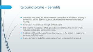
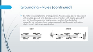
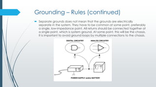
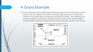
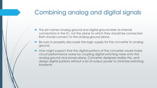
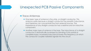
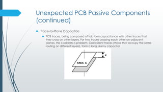
This document provides guidelines for laying out analog circuit boards to minimize noise. It recommends using multilayer boards with separate analog and digital ground and power planes. Traces should be short and avoid loops or 90 degree turns. Digital signals should be routed away from analog components. Bypass capacitors are needed at power inputs and op amps to filter different frequency ranges. Following these techniques can help reduce conducted and radiated noise by 20 decibels or more.
Report on PCB designing and fabrication by Prince RohanRohan Das
This is a report on our printed circuit board training on Central Mechanical Engineering Research Institute, Durgapur.
I hope this will help some student. Thank you
A printed circuit board (PCB) mechanically supports and electrically connects electronic components using conductive tracks, pads and other features etched from copper sheets laminated onto a non-conductive substrate.
High Voltage PCB Design Presentation by AltiumAltium
Looking for High Voltage PCB design resources?
Take a look at Altium's resources for electrical engineers and PCB designers here.
Or view the original presentation at: https://resources.altium.com/presentations/high-voltage-pcb-design-presentation
Or for even more information on High Voltage PCB Design, click here:
https://resources.altium.com/pcb-design-blog/high-voltage-pcb-design-creepage-and-clearance-distance
PCB Design using Eagle by Abdul Munaff & Prof. Anil KadleABDUL MUNAFF
A printed circuit board is used to mechanically support and electrically connect electronic components using conductive pathways (tracks).
Evolution of PCB.
Types of PCB- Single, Double Layer.
EAGLE Schematic Editor, Layout Editor, and Autorouter.
Basic terms related to Schematic, PCB Layout.
Designing process of printed circuit boardselprocus
Most key element in electronic circuits and equipment’s is the Printed Circuit Board which connects electronic components with conductive lines printed
Step by step guide which will help to understand the PCB fabrication process. PCB manufacturing and assembly must be conducted in a clean environment that is free of contaminants. This is important to produce good quality boards that offer unfailing service for years.
First, the PCB board concept
PCB board is also known as the printed circuit board, is an important electronic component, is the support body of electronic components, is the provider of electrical connection of electronic components. As it is made using electronic printing, it is called a "printed" circuit board.
A printed circuit board(PCB) is a laminated sandwich structure of conductive and insulating layers.
Technological Trends in the Field of Circuit Board Design and ManufacturingToradex
Circuit boards are extensively used across in the electronics industry. So much so that nowadays a circuit board designer is expected to be also proficient in the manufacturing technology apart from understanding electrical engineering. Read this article which will provide you with an insight on the various current and emerging technological trends prevailing in the manufacture of printed circuit boards.
Discover the wonderful world of Arduino, Circuit Scribe, Snap Circuits, LightUp, and more to help gain an understanding and appreciation of circuitry and electronics without the hassles of soldering and the dangers of being shocked.
Saturn Electronics Corporation is a Top 10 U.S. domestic bare printed circuit board manufacturer providing low-to-high volume production as well as complex prototypes and advanced technologies such as blind and buried vias, heavy copper, PTFE hybrids for RFMW and metal core for LED thermal management.
We are professional PCB design & fabrication in Taiwan and India. We manufacture high precision, high density, and high reliability PCB up to complex multi-layered boards. We PARTNER with our customers and suppliers to provide a total test/design solution.
Learn an overview of design trends and designer challenges, simulator extensions for models and abstraction levels in PSpice, and examples of a coding algorithm models into PSpice PCB level cycle
This webinar is an introduction to Flex and Rigid–Flex Gerber layout design methods and requirements that differ from standard rigid board technology.
Prepare to review some of the unique elements of Flex and Rigid–Flex Gerber layout to ensure functionality and mechanically reliability that meets or exceeds the design requirements.
This article talks about the available IoT embedded antenna options and influencing factors analysis. How to choose an embedded antenna for IoT applications?
IoT projects rely on wireless connectivity, and the signal of the wireless connection depends on the chip itself as well as the antenna.
Wi-Fi is the preferred choice for portable devices or IP cameras, while industrial applications (such as remote monitoring, smart meters, smart buildings, smart cities, manufacturing automation, smart agriculture, and tracking) are more likely to use LPWAN networks such as NB-IoT, LoRa, SigFox, ISM or cellular networks. Each of these types of networks has a wide variety of embedded antennas.
This article will discuss the embedded antenna options available and some of the factors that influence selection.
This article introduces the design of the antenna and recommends two tested low-cost PCB antennas. These PCB antennas can be used with Bluetooth Low Energy (BLE) solutions. For the best performance, BLE and BLE 2.4GHz radio frequencies must be correctly matched to their antennas.
At very high frequencies, every trace and pin is an RF emitter and receiver. If careful design practices are not followed, the unwanted signals can easily mask those a designer is trying to handle. The design choices begin at the architecture level and extend down to submillimeter placement of traces. There are tried and proven techniques for managing this process. The practical issues of real system design are covered in this session, along with ways to minimize signal degradation in the RF environment.
Implementation of Simple Wireless NetworkNiko Simon
End of course project where students were given free rein to explore wireless concepts through analysis of theory and hardware builds. The transmitter sends a Morse code audio signal which is then outputted by the receiver. Test of Morse code output: https://youtu.be/-06qOH7lYCg
Similar to Circuit Board Layout Techniques - www.circuitsinc.tk (20)
Welcome to the Program Your Destiny course. In this course, we will be learning the technology of personal transformation, neuroassociative conditioning (NAC) as pioneered by Tony Robbins. NAC is used to deprogram negative neuroassociations that are causing approach avoidance and instead reprogram yourself with positive neuroassociations that lead to being approach automatic. In doing so, you change your destiny, moving towards unlocking the hypersocial self within, the true self free from fear and operating from a place of personal power and love.
2. Introduction
Analog circuitry must be partitioned in its own section of the board, using
special layout techniques..
The common design mistakes of digital circuitry cannot be corrected by
the cut and jumper method for analog circuitry.
3. Noise sources
Conducted Emissions — noise that the analog circuitry generates through
its connections to other circuits. Negligible for low power circuits.
Radiated Emissions — noise that the analog circuitry generates, or
transmits, through the air. Negligible for low frequency operations.
Conducted Susceptibility — noise from external circuitry that is conducted
into the analog circuit through its connections to other circuits. Analog
circuitry must be connected to the ―outside world‖ by at least a ground
connection, a power connection, an input, and an output. Noise can be
conducted into the circuit through all of these paths, as well as any others
that are present.
4. Noise sources (continued)
Radiated Susceptibility — noise that is received through the air (or
transmitted into the analog circuitry) from external sources. Analog
circuitry, in many cases, resides on a PCB that may have high-speed digital
logic including DSP chips. High-speed clocks and switching digital signals
create considerable radio frequency interference (RFI). Other sources of
radiated noise are endless: the switching power supply in a digital
system, cellular telephones, broadcast radio and TV, fluorescent
lighting, nearby PCs, lightning in thunderstorms, and so on. Even if the
analog circuitry is primarily audio in frequency, RFI may produce noticeable
noise in the output.
5. PCB material
GRADE DESIGNATION MATERIAL/COMMENTS
FR–1 Paper/phenolic: room temperature punchable, poor moisture
resistance.
FR–2 Paper/phenolic: suitable for single-sided PCB consumer
equipment, good moisture resistance.
FR–3 Paper/epoxy: designed for balance of good mechanical and
electrical characteristics.
FR–4 Glass cloth/epoxy: excellent mechanical and electrical
properties.
FR–5 Glass cloth/epoxy: high strength at elevated temperatures,
self-extinguishing.
G10 Glass cloth/epoxy: high insulation resistance, highest bond
strength of glass laminates,
high humidity resistance.
G11 Glass cloth/epoxy: high flexural strength retention at high
temperature, extreme resistance to solvents
6. PCB material (continued)
Do not use FR–1.
FR–4 is commonly used in industrial-quality equipment, while FR–2 is used in
high-volume consumer applications. These two board materials appear to
be industry standards.
7. Layers of PCB
Single-Sided
Very simple consumer electronics are sometimes fabricated on single-sided
PCBs, keeping the raw board material inexpensive (FR–1 or FR–2) with thin copper
cladding.
This technique is only recommended for low-frequency circuitry. This type of
design is extremely susceptible to radiated noise.
Resistance in the power leads of the device must be taken into account, as well
as resistance between the return for the inputs and the load. Both the input and
load must return somewhere. If these are at different potentials due to trace
resistance, there can be problems.
8. Layers of PCB (continued)
Double-Sided
There are some double-sided FR–2 boards, they are more commonly fabricated
with FR–4 material. The increased strength of FR–4 material supports vias better.
Crossing traces on different layers is not recommended for analog circuitry.
Wherever possible, the bottom layer should be devoted to a ground plane, and
all other signals routed on the top layer.
9. Layers of PCB (continued)
Multi-layered
Critical designs call for multi-layer boards. Some of the reasons are :
Better routing for power as well as ground connections. If the power is also
on a plane, it is available to all points in the circuit simply by adding vias.
Other layers are available for signal routing, making routing easier.
There will be distributed capacitance between the power and ground
planes, reducing high frequency noise.
Other reasons which may not be intuitive:
Better EMI/RFI rejection. When a conductor is placed close to a parallel
conductive surface, most of the high frequency currents will return directly
under the conductor, flowing in the opposite direction. This transmission line
type setup is relatively immune to radiated noise.
Reduced overall project cost for small production runs. Although multi-layer
boards are more expensive to manufacture, EMI/RFI requirements from the
FCC or other agencies may require expensive testing of the design.
10. Layers of PCB (continued)
It is far better to take advantage of the distributed capacitance between
the power and ground plane by making them internal.
Another advantage of placing the planes internally is that the signal traces
are available for probing and modification on the top and bottom layers.
Anyone who has had to change connections on buried traces will
appreciate this feature.
For more than four layers, it is a general rule to shield higher speed signals
between the ground and power planes, and route slower signals on the
outer layers.
11. Ground plane - Benefits
Ground is frequently the most common connection in the circuit. Having it
continuous on the bottom layer usually makes the most sense for circuit
routing.
It increases mechanical strength of the board.
It lowers the impedance of all ground connections in the circuit, which
reduces undesirable conducted noise.
It adds a distributed capacitance to every net in the circuit — helping to
suppress radiated noise.
It acts a shield to radiated noise coming from underneath the board.
12. Grounding - Rules
Good grounding is a system-level design consideration. It should be
planned into the product from the first conceptual design reviews.
The Most Important Rule: Keep Grounds Separate
Separate grounding for analog and digital portions of circuitry is one of the
simplest and most effective methods of noise suppression. One or more layers on
multi-layer PCBs are usually devoted to ground planes.
More clarification in later slides.
Ground and power planes are at the same ac potential, due to
decoupling capacitors and distributed capacitance. Therefore, it is
important to isolate the power planes as well.
13. Grounding – Rules (continued)
Do not overlap digital and analog planes. Place analog power coincident
with analog ground, and digital power coincident with digital ground. If
any portion of analog and digital planes overlap, the distributed
capacitance between the overlapping portions will couple high-speed
digital noise into the analog circuitry.
14. Grounding – Rules (continued)
Separate grounds does not mean that the grounds are electrically
separate in the system. They have to be common at some point, preferably
a single, low-impedance point. All returns should be connected together at
a single point, which is system ground. At some point, this will be the chassis.
It is important to avoid ground loops by multiple connections to the chassis.
15. Grounding – Rules (continued)
It is important to keep digital signals away from analog portions of the
circuit. It makes little sense to isolate planes, keep analog traces short, and
place passive components carefully if there are high-speed digital traces
running right next to the sensitive analog traces. Digital signals must be
routed around analog circuitry, and not overlap analog ground and power
planes.
It is a good idea to locate analog circuitry as close as possible to the I/O
connections of the board. Digital designers, used to high current ICs, will be
tempted to make a 50-mil trace run several inches to the analog circuitry
thinking that reducing the resistance in the trace will help get rid of noise.
What they have actually done is create a long, skinny capacitor that
couples noise from digital ground and power planes into the op amp,
making the problem worse!
16. A Good Example
Three separate and isolated ground/power planes are employed: one for
power, one for digital, and one for analog. High-frequency conducted
noise on the power lines is limited by inductors (chokes). The designer has
even located low frequency analog circuitry close to low speed digital,
keeping high frequency digital and analog physically apart on the board.
17. Combining analog and digital signals
The pin names analog ground and digital ground refer to internal
connections in the IC, not the plane to which they should be connected.
Both should connect to the analog ground plane.
Be sure to properly decouple the logic supply for the converter to analog
ground.
One might suspect that the digital portions of the converter would make
circuit performance worse by coupling digital switching noise onto the
analog ground and power plane. Converter designers realize this, and
design digital portions without a lot of output power to minimize switching
transients
18. Unexpected PCB Passive Components
Trace Antennas
One basic type of antenna is the whip, or straight conductor. This
antenna works because a straight conductor has parasitic inductance,
and therefore can concentrate flux from external sources. The
impedance of any straight conductor has a resistive and an inductive
component.
Another major type of antenna is the loop. The inductance of a straight
conductor is dramatically increased by bending it into partial or
complete loops. Increased inductance lowers the frequency at which
the conductor couples radiated signals into the circuit.
19. Loops in a analog PCB design
Version A has a huge loop with no analog ground plane
Version B is better because of smaller loop area.
Version C is the best because of negligible loop area.
20. Unexpected PCB Passive Components
(continued)
Trace reflections
When a PCB trace turns a corner at a 90 degree angle, a reflection can occur.
This is primarily due to the change of width of the trace. At the apex of the turn,
the trace width is increased to 1.414 times its width. This upsets the transmission
line characteristics, especially the distributed capacitance and self–inductance
of the trace — resulting in the reflection.
21. Unexpected PCB Passive Components
(continued)
Trace-to-Plane Capacitors
PCB traces, being composed of foil, form capacitance with other traces that
they cross on other layers. For two traces crossing each other on adjacent
planes, this is seldom a problem. Coincident traces (those that occupy the same
routing on different layers), form a long, skinny capacitor
22. Unexpected PCB Passive Components
(continued)
Trace-to-Trace Capacitors and Inductors
PCB traces are not infinitely thin. They have some finite thickness, as defined by
the ounce parameter of the copper clad foil. The higher the number of ounces,
the thicker the copper. If two traces run side-by-side, then there will be
capacitive and inductive coupling between them.
23. Unexpected PCB Passive Components
(continued)
Inductive Vias
Whenever routing constraints force a via (connection between layers of a PCB, a
parasitic inductor is also formed.
24. Summary
General
Think of the PCB as a component of the design.
Know and understand the types of noise the circuit will be subjected to.
Prototype the circuit.
Board Structure
Use a high-quality board material such as FR–4.
Multi-layer boards are as much as 20-dB better than double-sided boards.
Use separate, non overlapping ground and power planes.
Place power and ground planes to the interior of the board instead of exterior.
25. Summary (continued)
Components
Be aware of frequency limitations of traces and other passive components.
Avoid vertical mounting of through-hole passive components in high-speed
circuits.
Use surface mount for high-speed analog circuitry.
Keep traces as short as possible.
Use narrow traces if long traces are required.
Terminate unused op amp sections properly.
26. Summary (continued)
Routing
Keep analog circuitry close to the power connector of the board.
Never route digital traces through analog sections of the board, or vice versa.
Make sure that traces to the inverting input of the op amp are short.
Make sure that traces to the inverting and noninverting inputs of the op amp do
not parallel each other for any significant length.
It is better to avoid vias, but the self-inductance of vias is small enough that a few
should cause few problems.
Do not use right angle traces, use curves if at all possible.
27. Summary (continued)
Bypass
Use the correct type of capacitor to reject the conducted frequency range.
Use tantalum capacitors at power input connectors for filtering power supply
ripple.
Use ceramic capacitors at power input connectors for high frequency
conducted noise.
Use ceramic capacitors at the power connections of every op amp IC package.
More than one capacitor may be necessary to cover different frequency ranges.
Change the capacitor to a smaller value — not larger — if oscillation occurs.
Add series inductors or resistors for stubborn cases.
Bypass analog power only to analog return, never to digital return.
28. References:
Excerpts from TI SLOA089
Op Amps for Everyone Literature Number: SLOD006A
Analog Dialog 30th Anniversary Issue, Analog Devices, Ask the Applications
Engineer–10, James Bryant
High-Speed Operational Amplifier Layout Made Easy, Texas Instruments,
Andy Hahn, SLOA046
Visit www.circuitsinc.tk and get your PCB designed for free!