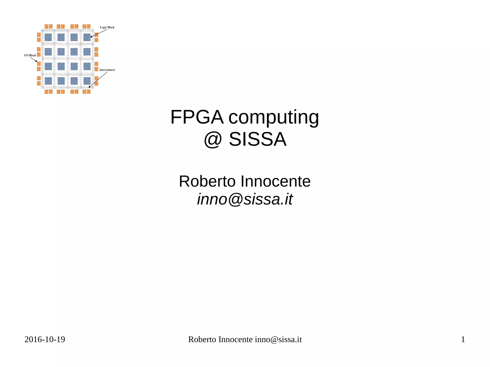
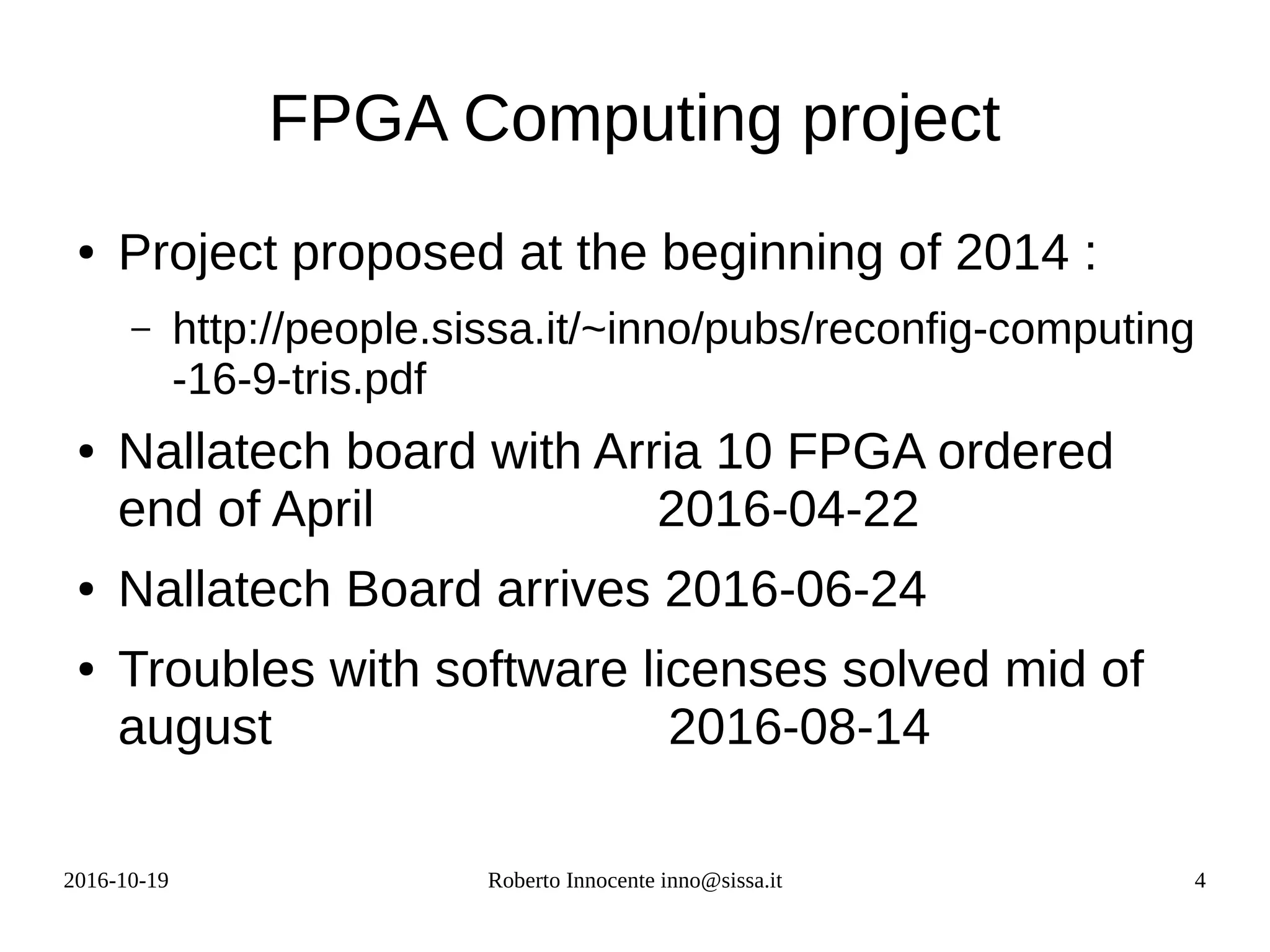
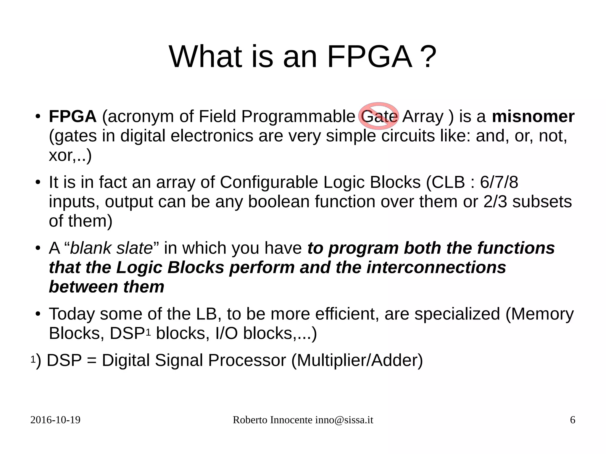
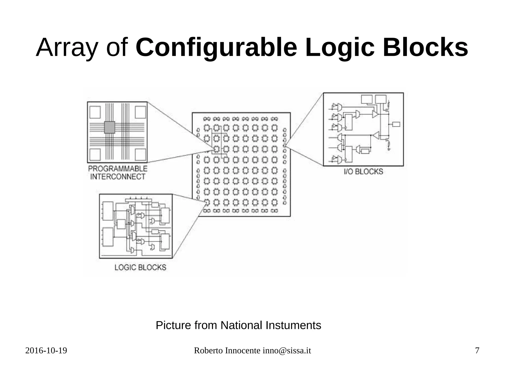
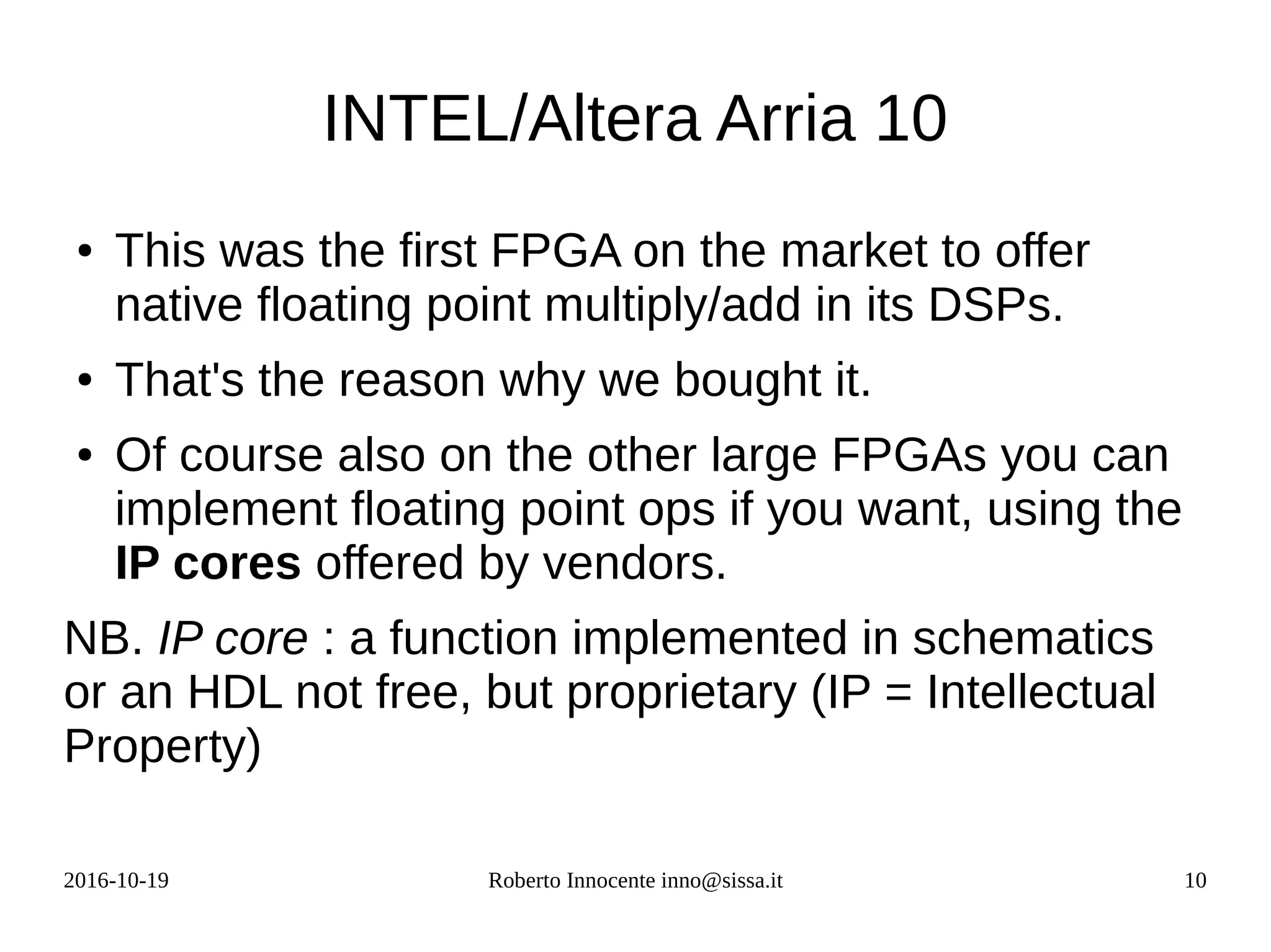
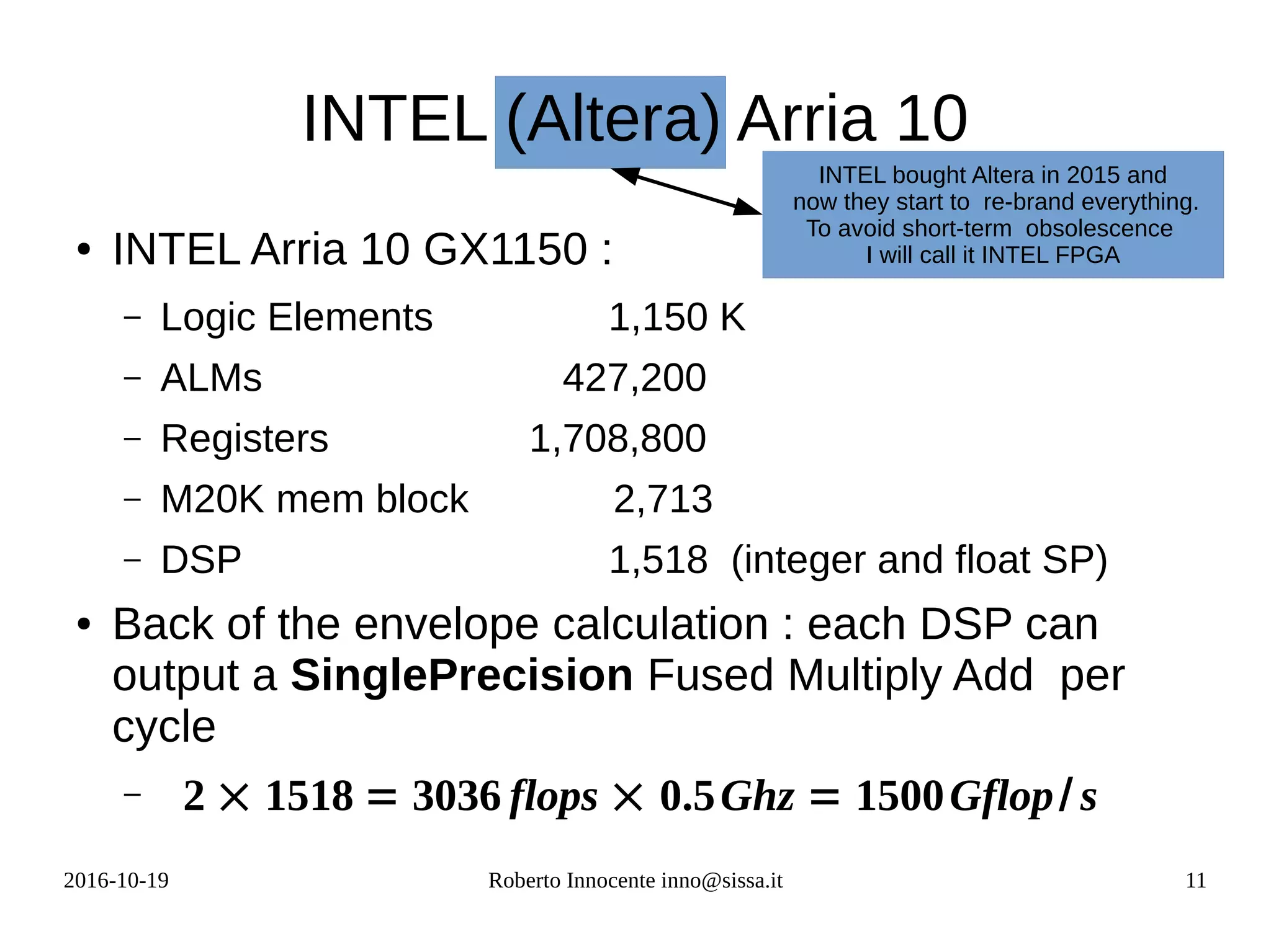
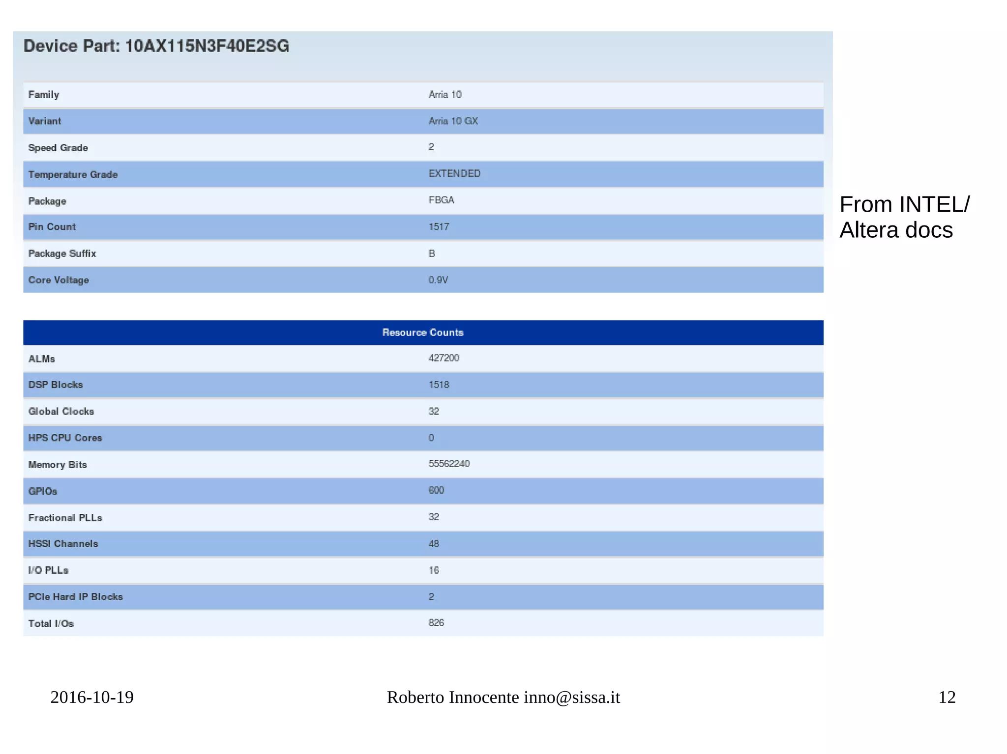
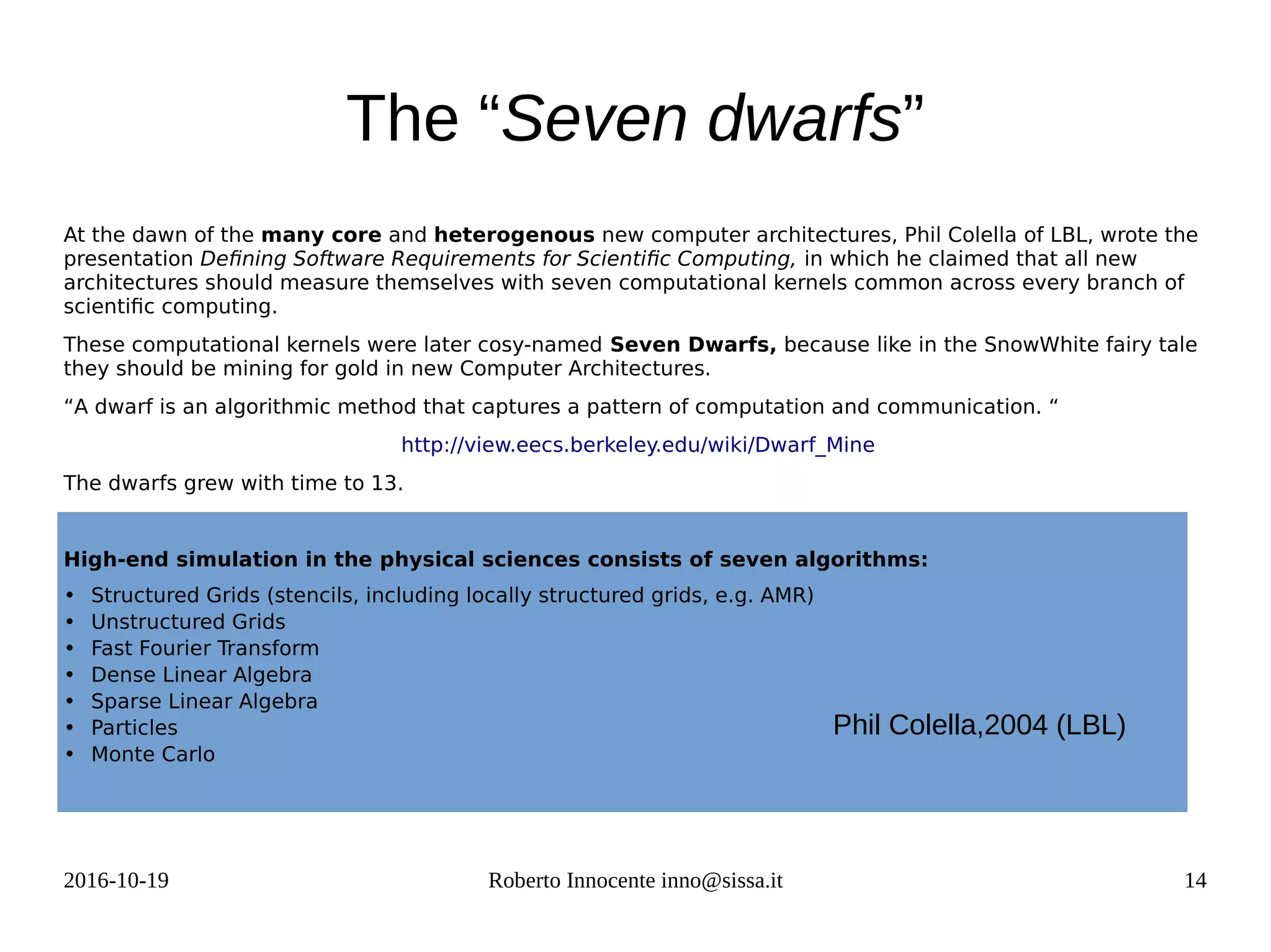
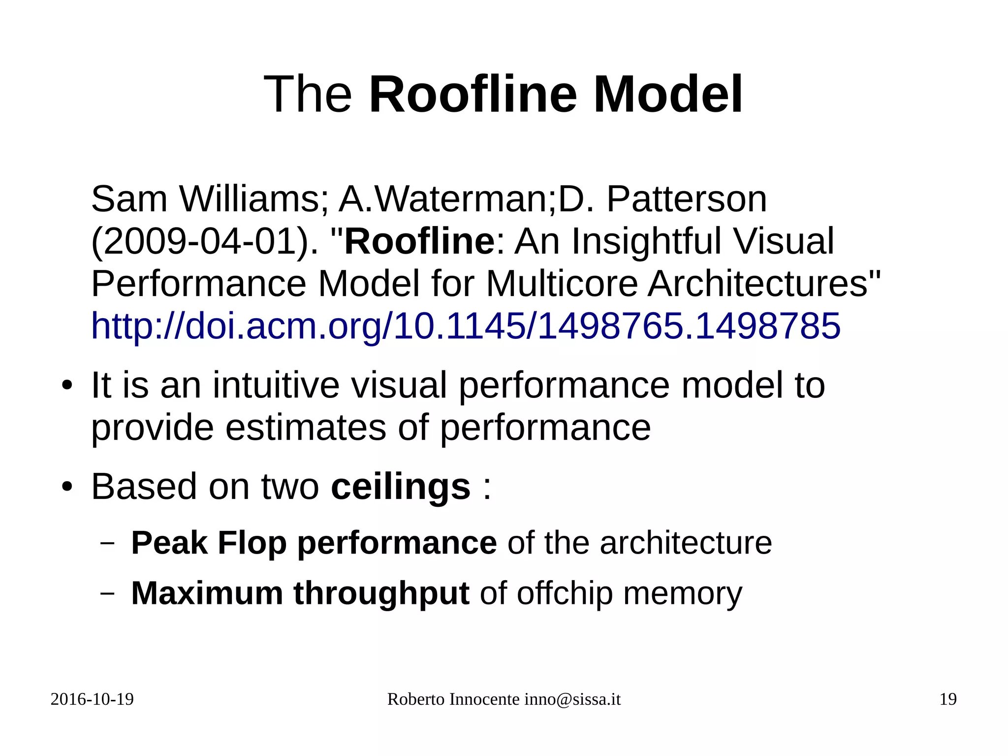
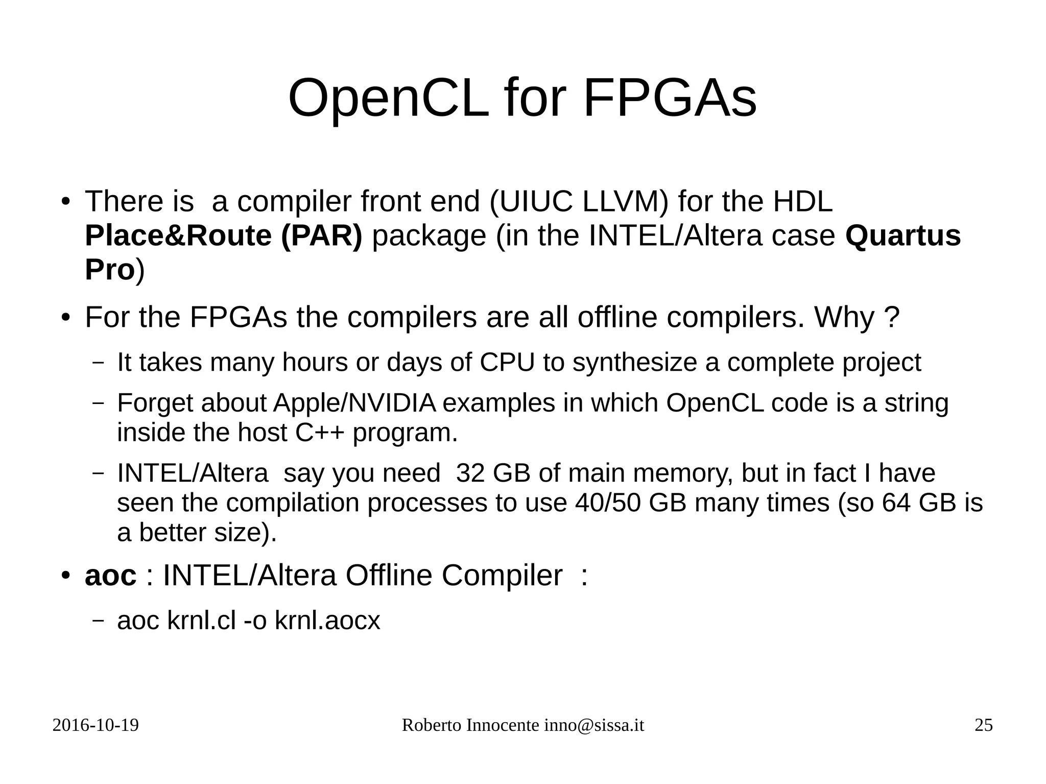
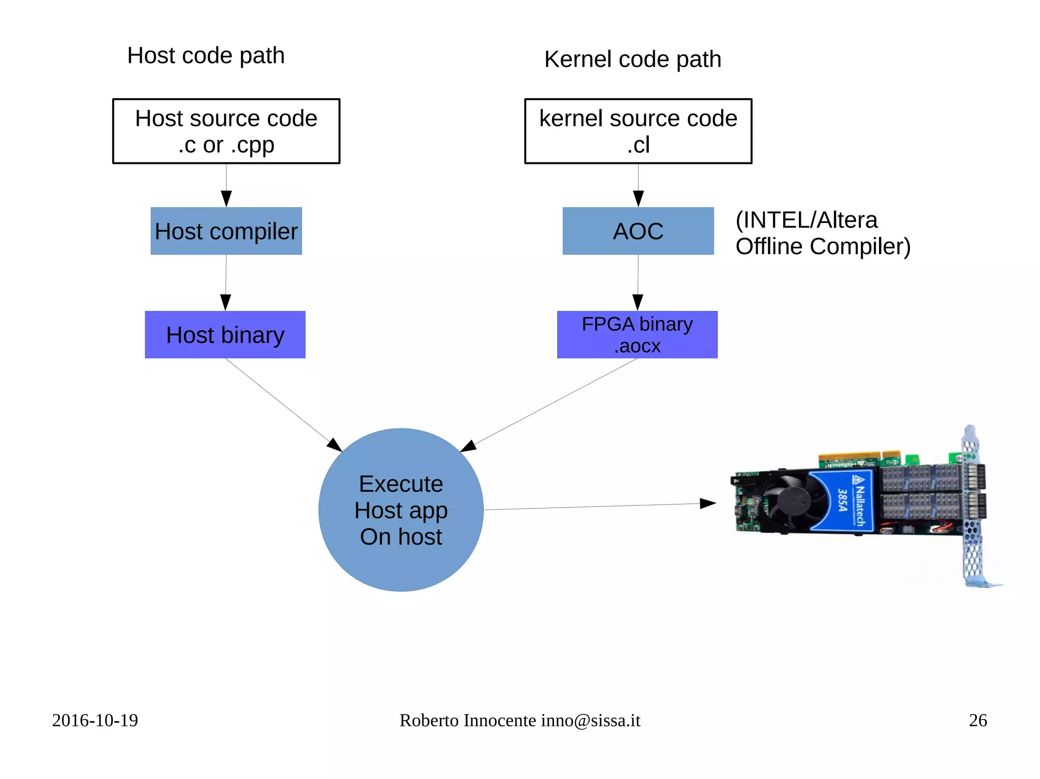
This document provides an overview of FPGA computing using an Intel/Altera Arria 10 FPGA. It begins with the history of the FPGA computing project and defines what an FPGA is. It then discusses the Intel Arria 10 FPGA used in tests. To measure performance on new architectures, it introduces the concept of the "Seven Dwarfs" benchmark algorithms and arithmetic intensity. The Roofline performance model is explained as a way to estimate performance based on peak flop rate and memory bandwidth. Actual performance results are shown for algorithms like vector addition, stencil code, and matrix multiplication run on the FPGA compared to CPU. OpenCL is discussed as a programming model for FPGAs.


![2016-10-19 Roberto Innocente inno@sissa.it 8
Scalar Product on an FPGA
x[0]
*
x[1]
*
x[2]
*
x[3]
*
y[0] y[1] y[2] y[3]
+ +
+
x . y = Sum x[i]*y[i]
DFG = Data Flow Graph
While with other
architectures you need to
adapt your program to the
architecture, with FPGA you
adapt the architecture to
your program.
Each cycle
a new result
after 7 flops](https://image.slidesharecdn.com/fpga-computing-161206142742/75/Fpga-computing-8-2048.jpg)
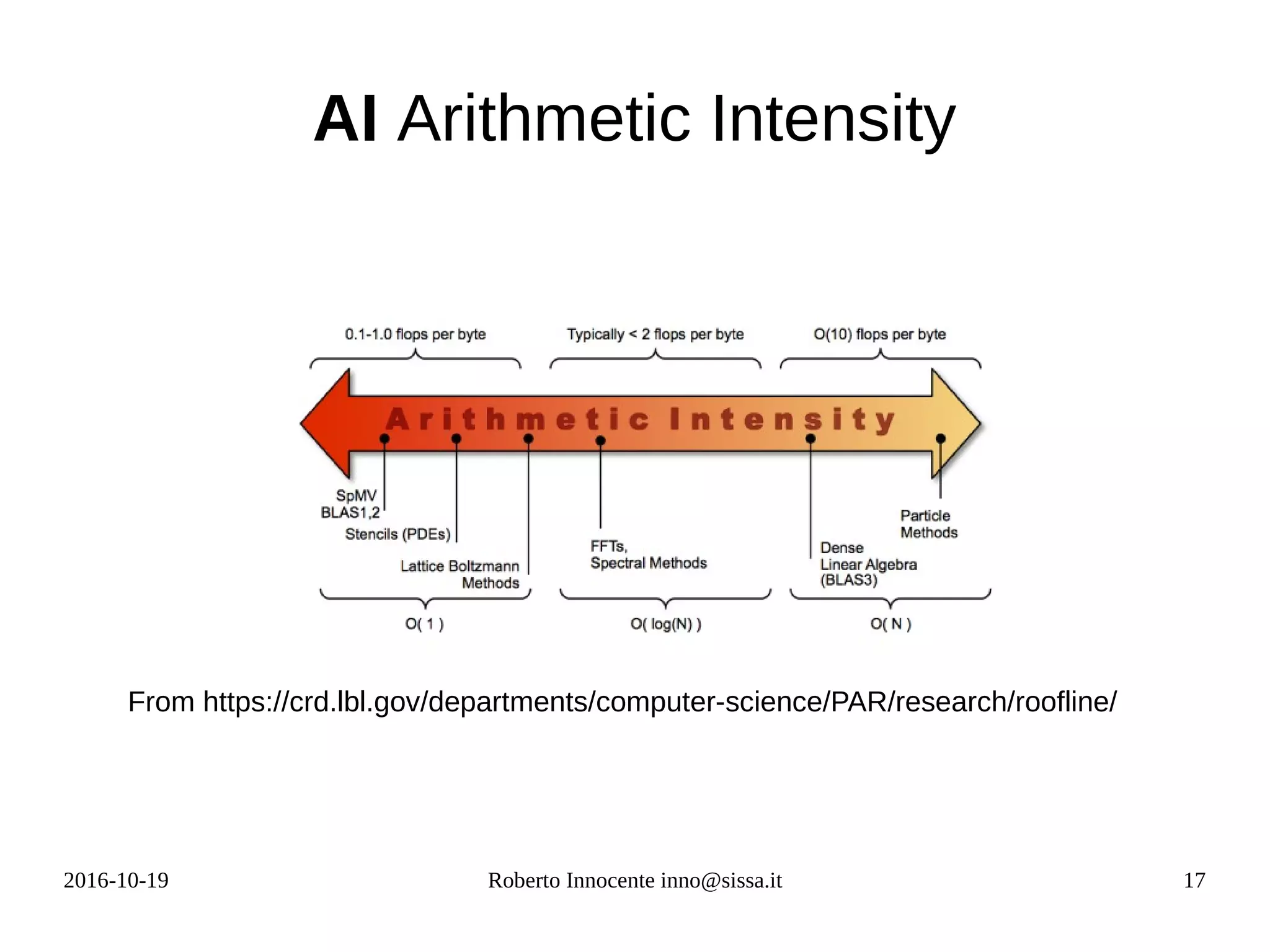
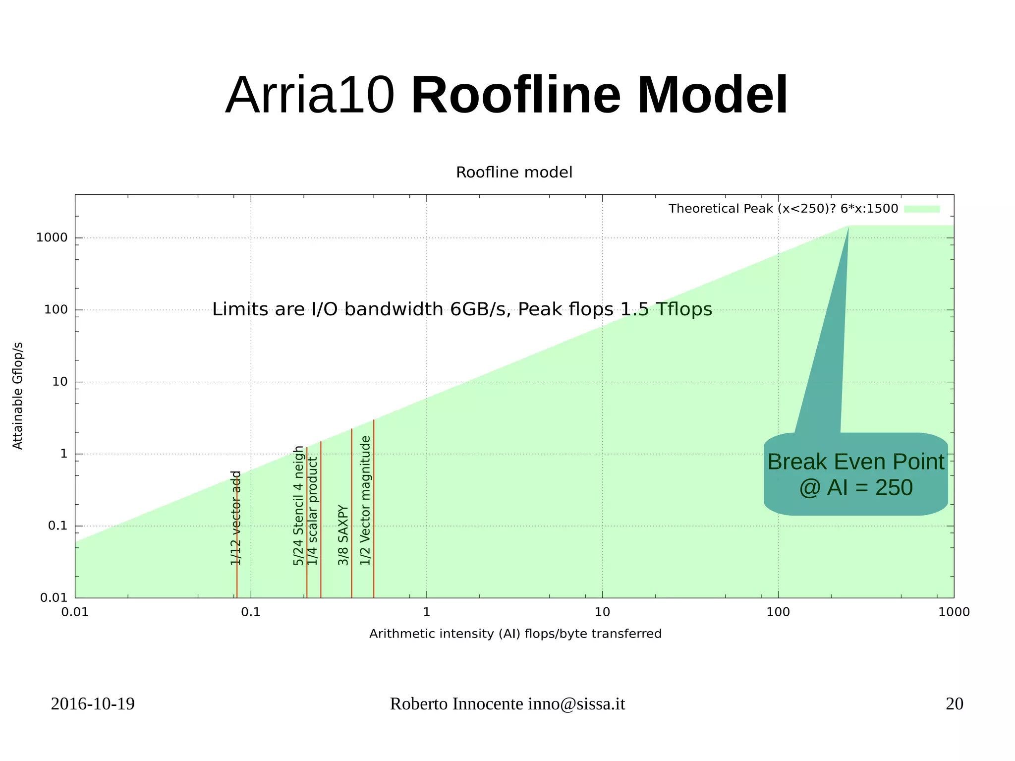
![2016-10-19 Roberto Innocente inno@sissa.it 16
Arithmetic/Computational Intensity (AI)
AI=
FLOPS
bytestransferred from/to offchip memory
AI
SingleP
AI
DoubleP
Vector addition z[i] = x[i] + y[i] 1/12 0.083 1/24
Scalar product Σ a[i] * b[i] ¼ 0.125 1/8
Vector magnitude Σ a[i] * a[i] ½ 0.500 ¼
SAXPY 1/6 0.375 1/12
Stencil 4 neighbors C[i,j] = a*A[i,j]
+b*(A[i-1,j]+A[i+1,j]...)
5/24 0.208 5/48
Matrix Multiply C[i,j] = Σk
A[k,i] * B[k,j] 1/4 0.125 1/8
FFT1d 0.9* log(N) 7.48
N=4096
α∗x+ y](https://image.slidesharecdn.com/fpga-computing-161206142742/75/Fpga-computing-16-2048.jpg)
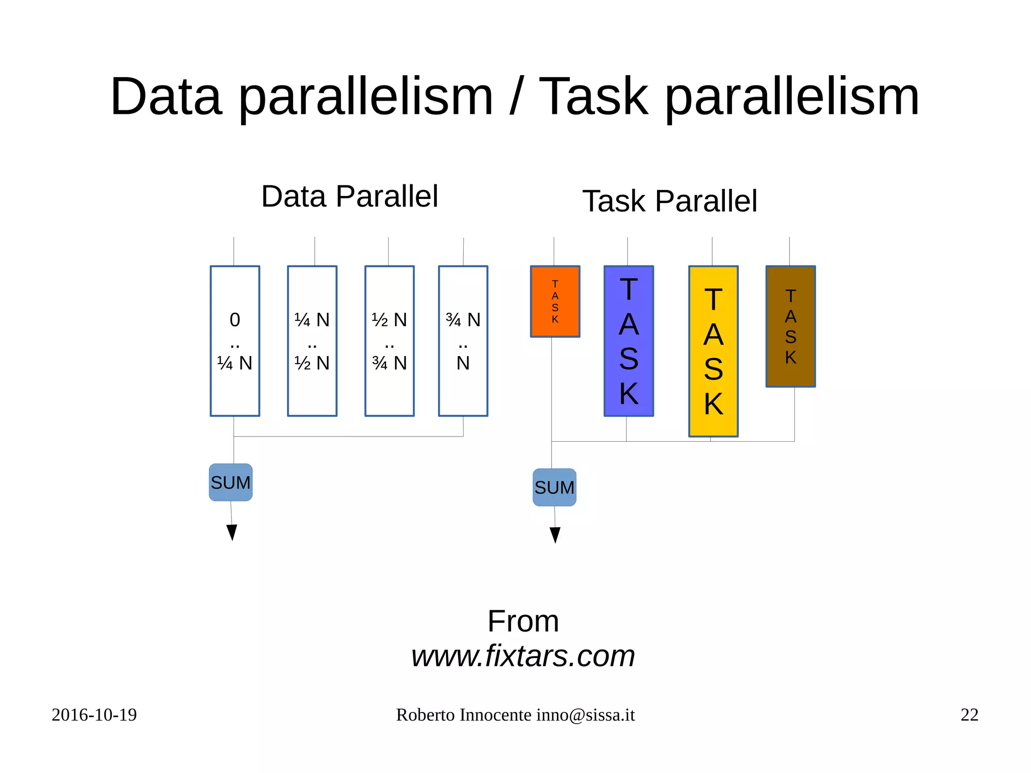
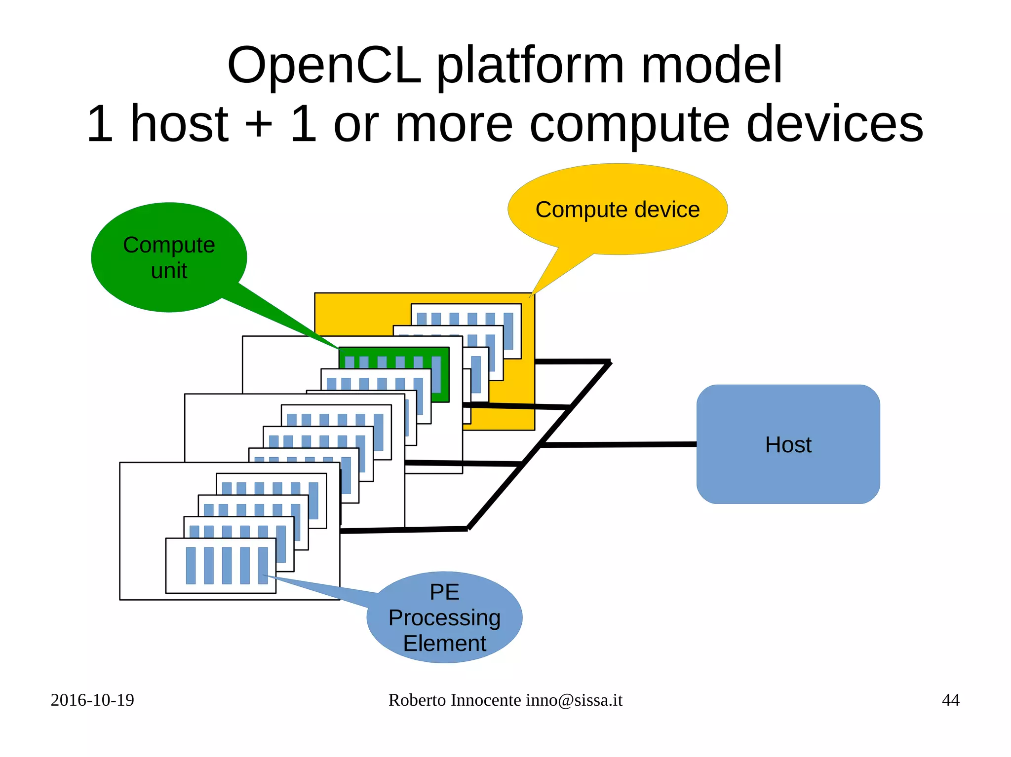
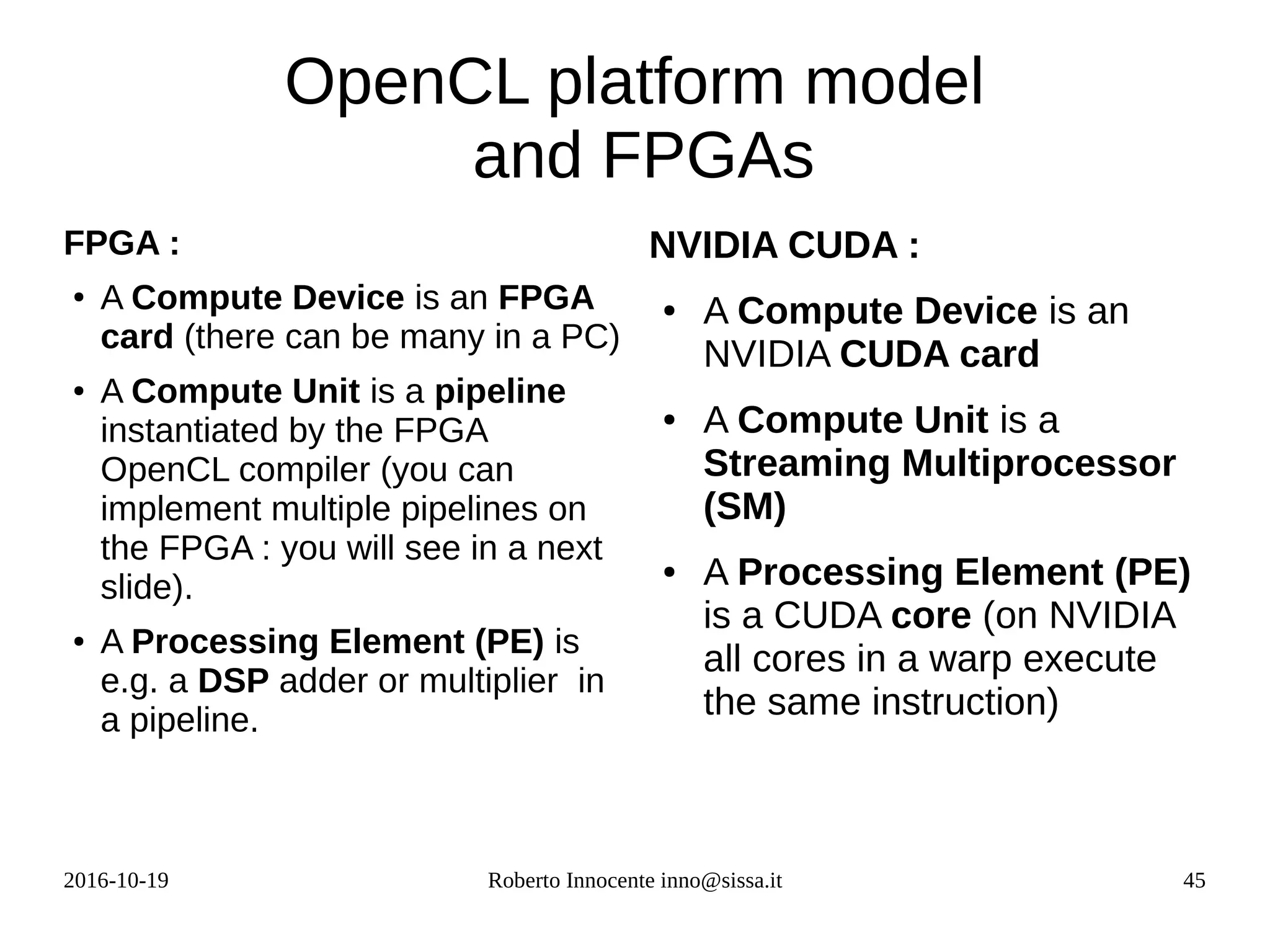
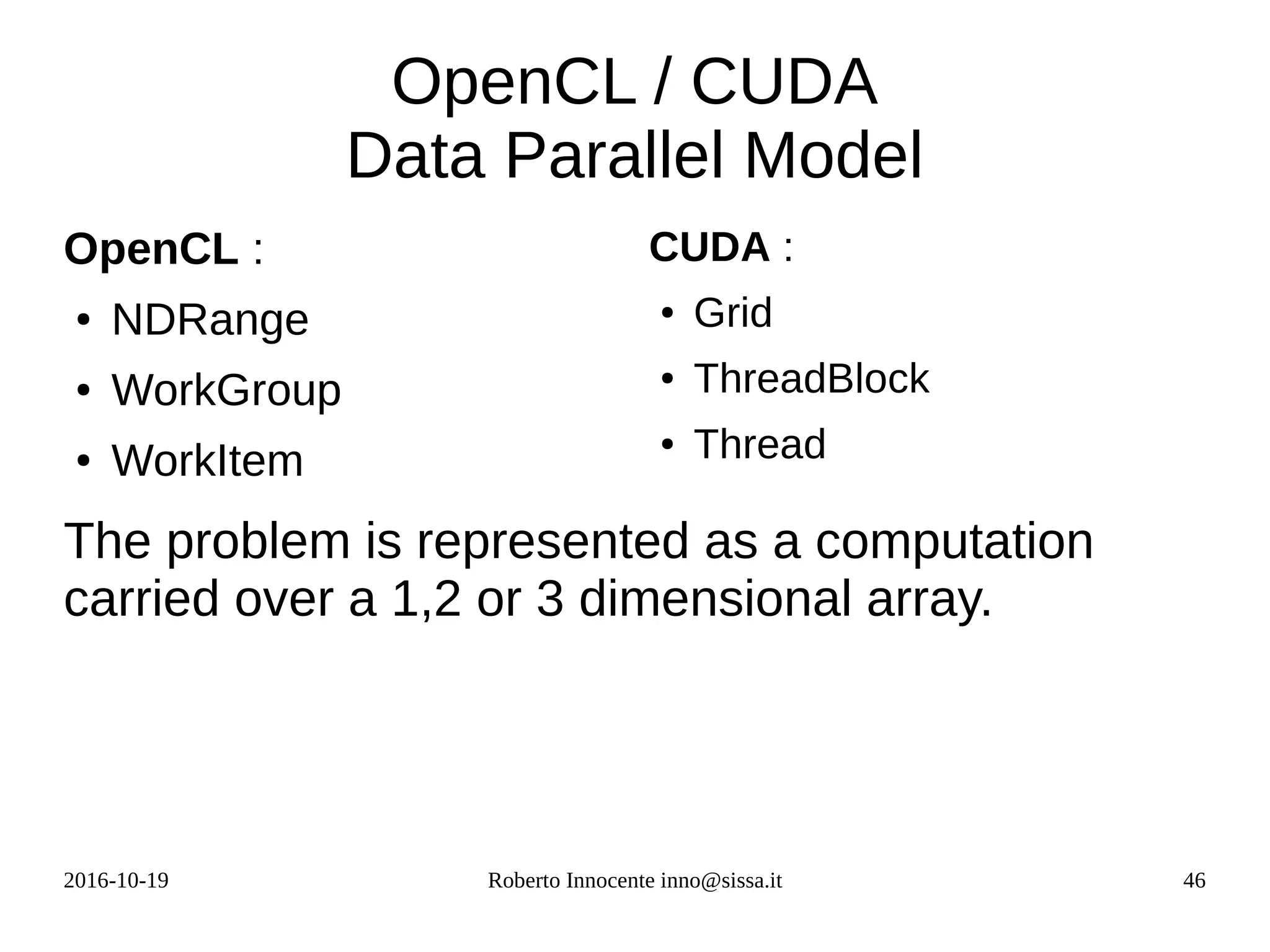
![2016-10-19 Roberto Innocente inno@sissa.it 23
The rise of the CUDA/OpenCL model
● In the mid of the past decade it was clear that Moore law could be respected only
through parallelism. ManyCore and Heterogenous computers appeared: GPUs,
FPGAs, CPUs, DSPs
●
GPUs with hundredths and then thousands of simple cores (forthcoming NVIDIA
pascal ~ 3.800 [available from 2017] )
● Data parallelism can be supported with a simple model (differently from task
parallelism) : a compute pattern (kernel) instantiated on every core with a
different set of indices.
– a[i]+b[i] (Vector Addition kernel)
– Σk a[i,k] * b[k,j] (Matrix multiplication kernel)
– 1 /2 /3 dimensional NDRange / grid
● Each instantiation (work-item/thread) is provided with different parameters
through a function call (e.g. get_global_id() , in fact the core computes
displacements by itself knowing its wg and wi numbers )](https://image.slidesharecdn.com/fpga-computing-161206142742/75/Fpga-computing-23-2048.jpg)
![2016-10-19 Roberto Innocente inno@sissa.it 30
Vector Addition
● z[i] = x[i] + y[i]
● Computational
intensity very low :
–
● Limit is then from I/O:
– 6 GB* 1/12 = 0.5
Gflops/s
./vector_add
Initializing OpenCL
Platform: Altera SDK for OpenCL
Performance on CPU 1 core of intel i7 :
Processing time on CPU = 1.1313ms
Mflops/s 883.948201
Launching for device 0 (1000000 elements)
Performance on FPGA :
Processing time on FPGA = 6.5348ms
Mflop/s on FPGA= 153.027972
Time: 6.535 ms
Kernel time (device 0): 3.668 ms
AI=
1
12](https://image.slidesharecdn.com/fpga-computing-161206142742/75/Fpga-computing-30-2048.jpg)
![2016-10-19 Roberto Innocente inno@sissa.it 39
Computing π with Montecarlo
Computes π with a Mersenne
twister rng.
Points = 222
GlobalWS=WG 32 , LocalWS=WI 32
I. 32x32 WI = 1024 generate 4096
rn in [0,1]x[0,1] = 222= 4194304
II.For each batch of 4096 rn
computes ins and outs respect to
the circle
III.Computes average
It takes ~ 854 ns for each rn
Using AOCX: mt.aocx
Reprogramming device with handle 1
Count all 26354932.000000 / ( rn
4096 * rng 32 *32) * 4
Computed pi = 3.141753
Mersenne twister : 1954.146849[ms]
Computing pi : 1632.340594[ms]
Copy results : 0.077611[ms]
Total time : 3586.565054[ms]](https://image.slidesharecdn.com/fpga-computing-161206142742/75/Fpga-computing-39-2048.jpg)
![2016-10-19 Roberto Innocente inno@sissa.it 40
Sobel filter
● 1920 x 1080 pixels image, 3 x 8 planes
color ~ 6 MB
●
Filter can be applied 140 fps
●
luma=(([R G B]
[
66
129
25 ]+128)≫8)+16 RecBT709
Sobel Operators Sx=
[
−1
−2
−1
0
0
0
1
2
1]Sy=
[
−1
0
+1
−2
0
+2
−1
0
+1]∂I
∂x
=I∗Sx ,
∂I
∂ y
=I∗Sy
∇I=[∂I
∂x
∂I
∂ y ], ‖∇ I‖=
√(∂I
∂ x)
2
+(∂ I
∂ y)
2
‖∇ I (i , j)‖ < θ → pixel(i, j)=(0,0,0)
Convolution](https://image.slidesharecdn.com/fpga-computing-161206142742/75/Fpga-computing-40-2048.jpg)
![2016-10-19 Roberto Innocente inno@sissa.it 49
Vector Addition/Matrix Multiplication
OpenCL kernels
// vector addition
C:
for(i=0;i<N;i++){
C[i] = A[i]+B[i];
}
OpenCL:
__kernel void vecadd(__global const float* A,
__global const float* B,
__global float* C)
{
i = get_global_id(0);
C[i] = A[i] + B[i];
}
// matrix multiplication
C:
for(i=0;i<N;i++){
for(j=0;j<N;j++){
Temp = 0.0f;
for(k=0;k<N;k++){
Temp += A[i][k] * B[k][j]
}
C[i][j] = Temp;
}
}
OpenCL:
__kernel void matmul(__global const float* A,
__global const float* B,
__global float* C, )
{
__local float sum;
i = get_global_id(0);
j = get_global_id(1);
sum = 0.0f;
for(k=0;k<N;k++) {
sum += A[i][k] * B[k][j];
}
C[i][j] = sum;
}](https://image.slidesharecdn.com/fpga-computing-161206142742/75/Fpga-computing-49-2048.jpg)

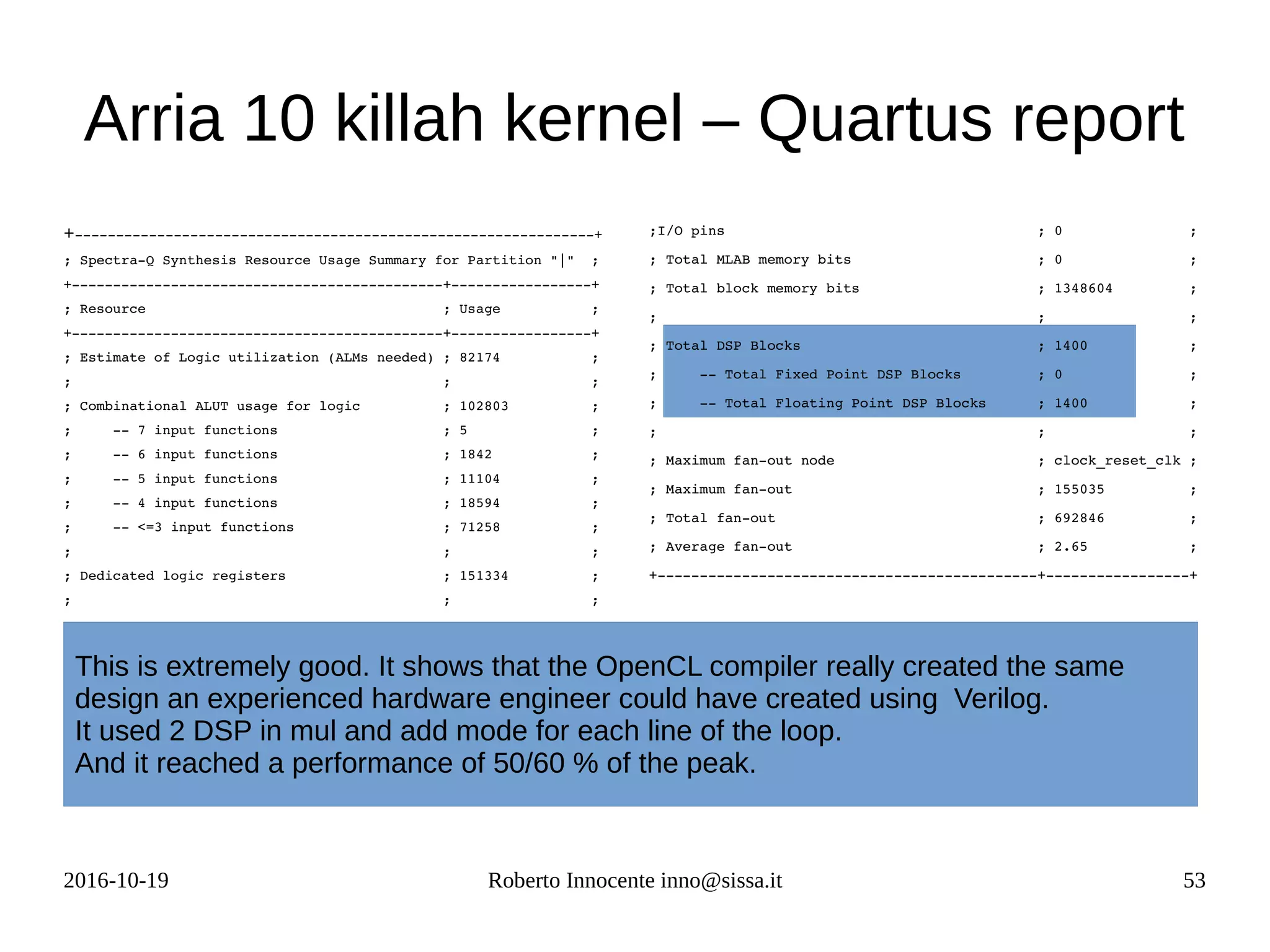
![2016-10-19 Roberto Innocente inno@sissa.it 52
Arria 10 killah kernel
Initializing OpenCL
Platform: Altera SDK for OpenCL
Using 1 device(s)
p385a_sch_ax115 : nalla_pcie (aclnalla_pcie0)
Using AOCX: loop.aocx
Reprogramming device with handle 1
Launching for device 0 (100000 elements)
Total runs 100000 , gflop 107374.182400
100,000 x 4 x (256*1024*1024)
Wall Time: 139909.012 ms
Gflop/s 767.457225
Kernel time (device 0): 139908.517 ms
Gflop/s 767.459945
2.0
* 2.0
+ 0.5
* 1.0
+
x[i]
res
#define N (256*1024*1024)
__kernel
void loop
(__global const float* x,
__global float *restrict y)
{
local float res;
int i = get_global_id(0);
res = x[i];
#pragma unroll 700
for(i=0;i<N;i++){
res = res*2.0f + 2.0f;
res = res*0.5f – 1.0f;
}
y[i] = res;
}](https://image.slidesharecdn.com/fpga-computing-161206142742/75/Fpga-computing-52-2048.jpg)

![2016-10-19 Roberto Innocente inno@sissa.it 59
top.v
module top( x0,y0,x1,y1,x2,y2,x3,y3,z,clk,ena,aclr);
input [31:0]x0; input [31:0]y0;
input [31:0]x1; input [31:0]y1;
input [31:0]x2; input [31:0]y2;
input [31:0]x3; input [31:0]y3;
output [31:0]z;
input clk; input ena; input [1:0]aclr;
wire [31:0]ir0; wire [31:0]ir1; wire [31:0]ir2; wire [31:0]ir3;
wire [31:0]ir4; wire [31:0]ir5;
dsp_fp_mul m1(.aclr(aclr),.ay(x0),.az(y0),.clk(clk),.ena(ena),.result(ir0));
dsp_fp_mul m2(.aclr(aclr),.ay(x1),.az(y1),.clk(clk),.ena(ena),.result(ir1));
dsp_fp_mul m3(.aclr(aclr),.ay(x2),.az(y2),.clk(clk),.ena(ena),.result(ir2));
dsp_fp_mul m4(.aclr(aclr),.ay(x3),.az(y3),.clk(clk),.ena(ena),.result(ir3));
dsp_fp_add a1(.aclr(aclr),.ax(ir0),.ay(ir1),.clk(clk),.ena(ena),.result(ir4));
dsp_fp_add a2(.aclr(aclr),.ax(ir2),.ay(ir3),.clk(clk),.ena(ena),.result(ir5));
dsp_fp_add a3(.aclr(aclr),.ax(ir4),.ay(ir5),.clk(clk),.ena(ena),.result(z));
endmodule
top.v
dsp_fp_add.v
a1
dsp_fp_mul.v
m4
dsp_fp_mul.v
m1
dsp_fp_mul.v
m3
dsp_fp_mul.v
m2
dsp_fp_add.v
a3
dsp_fp_add.v
a2
In Verilog what seems a function call in fact is an instantiation of a
circuit inside another. The parameter syntax represents the
correspondence (connection) of wires with wires.](https://image.slidesharecdn.com/fpga-computing-161206142742/75/Fpga-computing-59-2048.jpg)
![2016-10-19 Roberto Innocente inno@sissa.it 60
dsp_fp_xxx
// dsp_fp_mul.v
// Generated using ACDS version 16.0 211
`timescale 1 ps / 1 ps
module dsp_fp_mul (
input wire [1:0] aclr, // aclr.aclr
input wire [31:0] ay, // ay.ay
input wire [31:0] az, // az.az
input wire clk, // clk.clk
input wire ena, // ena.ena
output wire [31:0] result // result.result
);
dsp_fp_mul_altera_fpdsp_block_160_ebvuera fpdsp_block_0 (
.clk (clk), // clk.clk
.ena (ena), // ena.ena
.aclr (aclr), // aclr.aclr
.result (result), // result.result
.ay (ay), // ay.ay
.az (az) // az.az
);
endmodule
// dsp_fp_add.v
`timescale 1 ps / 1 ps
module dsp_fp_add (a,b,c,clk,ena,aclr);
input wire [31:0]a;
input wire [31:0]b;
output wire [31:0]c;
input wire clk;
input wire ena;
input wire [1:0]aclr;
dsp_fp_add_altera_fpdsp_bloc_160_nmfrqti fdsp_block_0 (
.clk (clk),
.ena(ena),
.aclr(aclr),
.ax (a), // ax.ax
.ay (b), // ay.ay
.result (c) // result.result
);
endmodule
dsp_fp_mul.v dsp_fp_add.v
These 2 modules are generated automatically when you instantiate
from the IP cores a DSP in floating point mode and configure it like
an adder or a multiplier](https://image.slidesharecdn.com/fpga-computing-161206142742/75/Fpga-computing-60-2048.jpg)
![2016-10-19 Roberto Innocente inno@sissa.it 62
System Verilog1
– Killah kernel
sp_12.sv
module sp_12
#( parameter N=700)
(
input logic [31:0]x,
output logic [31:0]out,
input logic clk,ena,
input logic [1:0]aclr
);
logic [31:0] mul_2,add_2,
mul_05,sub_1;
logic [31:0]ir[2*N+4];
assign mul_2 = shortreal'(2.0);
assign add_2 = shortreal'(2.0);
assign mul_05 = shortreal'(0.5);
assign sub_1 = shortreal'(-1.0);
assign ir[0] = x;
genvar i;
generate
for(i=0;i<=N;i=i+1)
begin: FMA2_LOOP
dsp_fp_fma inst (
.ax(add_2),
.ay(ir[2*i]),
.az(mul_2),
.result(ir[2*i+1]),
.clk(clk),
.ena(ena),
.aclr(aclr)
);
dsp_fp_fma inst1(
.ax(add_2),
.ay(ir[2*i+1]),
.az(mul_2),
.result(ir[2*i+2]),
.clk(clk),
.ena(ena),
.aclr(aclr)
);
end
endgenerate
assign out = ir[2*N+2];
endmodule
Quartus report :
1,402 DSP used1)
SystemVerilog is a new edition of
Verilog (1800-2012) with many additions](https://image.slidesharecdn.com/fpga-computing-161206142742/75/Fpga-computing-62-2048.jpg)
![2016-10-19 Roberto Innocente inno@sissa.it 63
// dsp_fp_fma.v
// Generated using ACDS version 16.0 211
`timescale 1 ps / 1 ps
module dsp_fp_fma (
input wire [1:0] aclr, // aclr.aclr
input wire [31:0] ax, // ax.ax
input wire [31:0] ay, // ay.ay
input wire [31:0] az, // az.az
input wire clk, // clk.clk
input wire ena, // ena.ena
output wire [31:0] result // result.result
);
dsp_fp_fma_altera_fpdsp_block_160_fj4u2my fpdsp_block_0 (
.clk (clk), // clk.clk
.ena (ena), // ena.ena
.aclr (aclr), // aclr.aclr
.result (result), // result.result
.ax (ax), // ax.ax
.ay (ay), // ay.ay
.az (az) // az.az
);
endmodule
Verilog : dsp_fp_fma.v
This file is generated
automatically when you
instantiate a DSP as a
multiplier/adder with the
parameter editor. It differs
from the others that
resulted from single
operation instantiation (like
only mul or only add) : it
uses all 3 input busses as
you can see.](https://image.slidesharecdn.com/fpga-computing-161206142742/75/Fpga-computing-63-2048.jpg)
![2016-10-19 Roberto Innocente inno@sissa.it 66
My Proposal: json-graph-fpga
Use a simple and already
existing format to describe the
graph of components. Json for
instance, or Json-graph. (We
assume all components become
connected to a global clock)
{
“inputs”:[“x0”,”x1”,”x2”,”x3”,
“y0”,”y1”,”y2”,”y3”],
“x0”:[“m1”],“y0”:[“m1”],
“x1”:[“m2”],”y1”:[“m2”],
“x2”:[“m3”],”y1”:[“m3”],
“x3”:[“m4”],”y1”:[“m4”],
“m1”:[“a1”],”m2”:[“a1”],
“m3”:[“a2”],”m4”:[“a2”],
“a1”:[“a3”],”a2”:[“a3”],
“a3”:[“outputs”]
}
I
n
p
u
t
s
O
u
t
p
u
t
s
*
m1
*
m2
*
m3
*
m4
+
a1
+
a2
+
a3](https://image.slidesharecdn.com/fpga-computing-161206142742/75/Fpga-computing-66-2048.jpg)