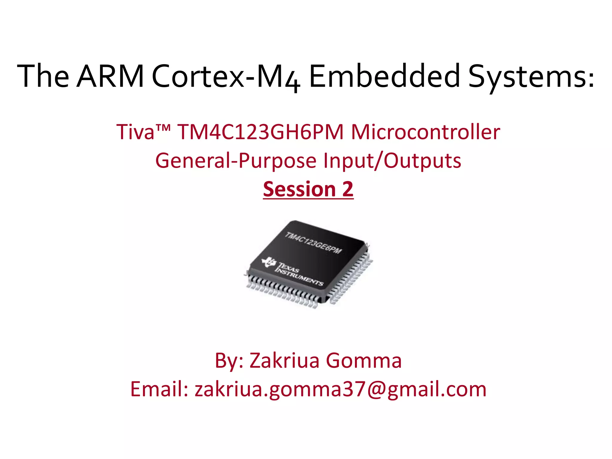
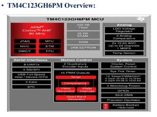
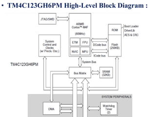
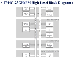
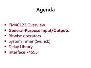
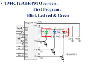
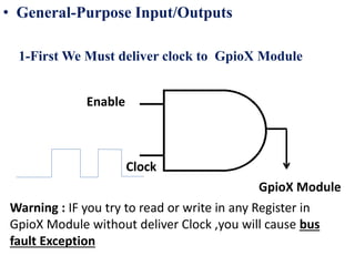
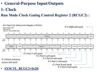
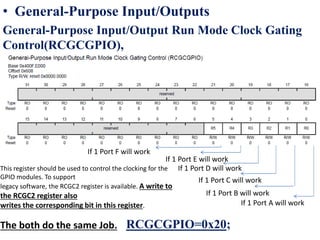
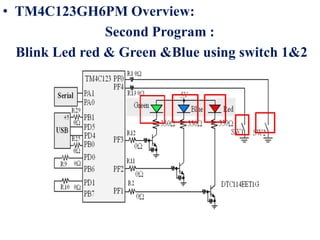
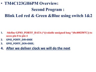
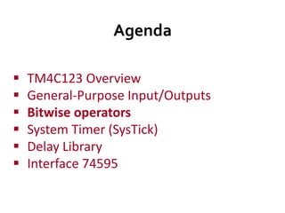
This document provides an overview and agenda for a presentation on the ARM Cortex-M4 embedded system and the Tiva TM4C123GH6PM microcontroller. The presentation covers the microcontroller overview, general purpose input/outputs, bitwise operators, the system timer SysTick, delay libraries, and interfacing with the 74595 chip. The agenda includes slides on each of these topics.
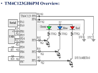
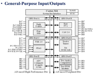
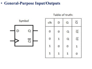
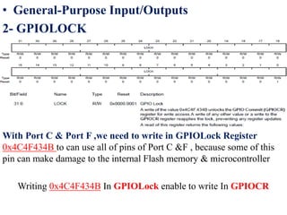
![• General-Purpose Input/Outputs
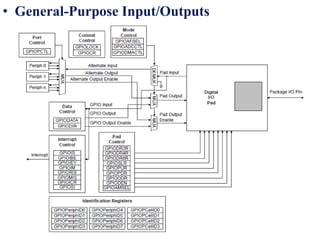
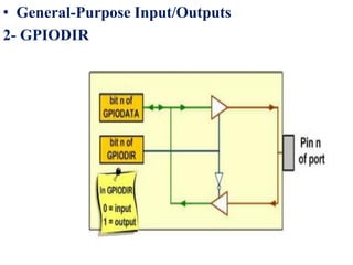
3- GPIOCR
This register is designed to prevent accidental programming
of the registers that control connectivity to the NMI and
JTAG/SWD debug hardware. By initializing the bits of the
GPIOCR register to 0 for PD7, PF0, and PC[3:0].](https://image.slidesharecdn.com/second-160916193832/85/GPIO-In-Arm-cortex-m4-tiva-c-27-320.jpg)


![[Deck] What's New in Spark-Iceberg Integration via DSV2.pptx](https://cdn.slidesharecdn.com/ss_thumbnails/deckwhatsnewinspark-icebergintegrationviadsv2-260210005337-25955b12-thumbnail.jpg?width=640&height=640&fit=bounds)


