Downloaded 146 times
![Combinational Logic
Circuit
Yong Heui Cho @ Mokwon University
Some of slides are referred to:
[1] 전재욱, 논리회로 설계실험, 성균관대학교.
[2] Imran Waris, Digital and Logic Design, slideshare, 2014.](https://image.slidesharecdn.com/4-151001115025-lva1-app6891/85/Combinational-Logic-Circuit-1-320.jpg)


![17
Analog AND Gate Circuit
17
B
C
E
=>
B
C E
Output
Input A Input B
< TR > < Switch >
□ Courtesy to 전재욱, 논리회로 설계실험, 성균관대학교.
An AND gate is series wire connection!
+5 [V]](https://image.slidesharecdn.com/4-151001115025-lva1-app6891/85/Combinational-Logic-Circuit-17-320.jpg)

![19
Analog OR Gate Circuit
19
Input A Input B
Output
□ Courtesy to 전재욱, 논리회로 설계실험, 성균관대학교.
An OR gate is parallel wire connection!
+5 [V]](https://image.slidesharecdn.com/4-151001115025-lva1-app6891/85/Combinational-Logic-Circuit-19-320.jpg)


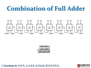
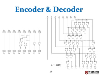
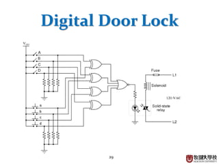

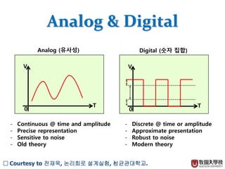
The document discusses combinational logic circuits. It begins with an introduction to analog and digital signals and binary number systems. It then covers Boolean algebra and logic gates such as AND, OR, NAND, NOR, XOR and XNOR. Combinational logic circuits are classified and examples like half adders, full adders, encoders and decoders are presented. One application discussed is a digital door lock circuit using logic gates.