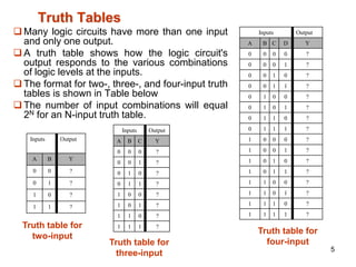
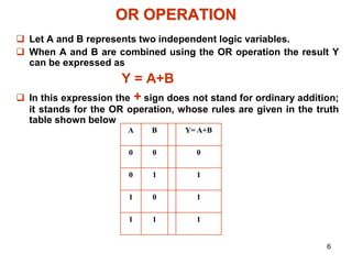
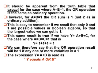
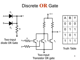
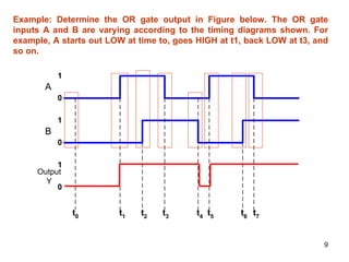
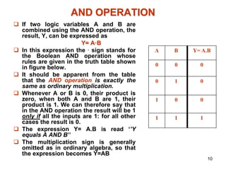
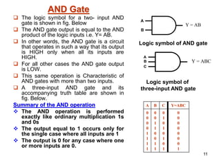
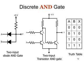
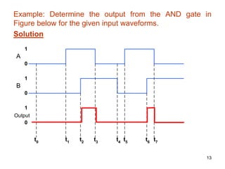
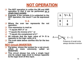
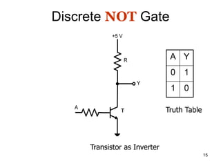
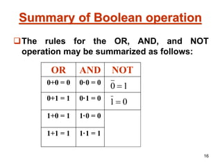
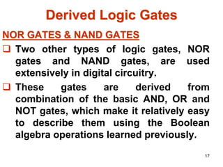
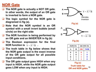
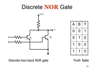
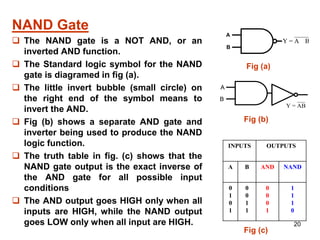
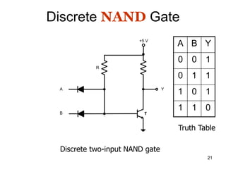
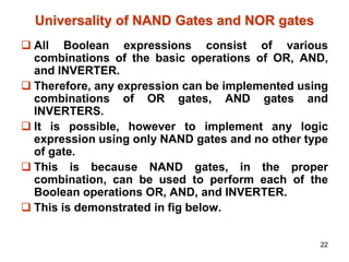
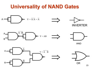
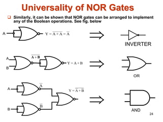
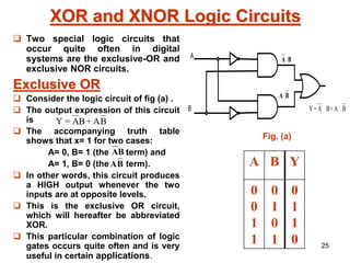
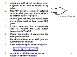
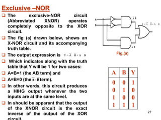
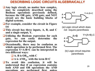
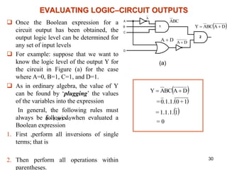
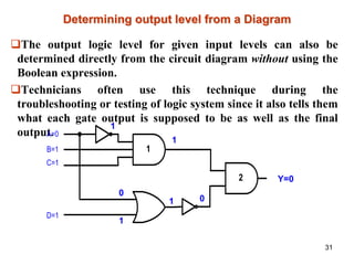
The document discusses basic and derived logic gates. It begins by introducing Boolean algebra and defining logic 0 and 1. It then explains the three basic logic gates - OR, AND, and NOT - through truth tables and circuit diagrams. The OR gate's output is 1 if any input is 1. The AND gate's output is 1 only if all inputs are 1. The NOT gate inverts the input. Complex logic circuits can be described algebraically using these basic gates and Boolean operations.
This document discusses digital logic gates. It begins by defining a gate as a digital circuit with one or more inputs and one output. The three basic gates are described as the NOT, OR, and AND gates. Additional universal gates, the NAND and NOR gates, are introduced. Truth tables are provided to explain the output of each gate for all possible input combinations. The document also discusses how to derive different gate functions using NAND and NOR gates alone through De Morgan's theorems.
This document describes several basic digital logic gates - AND, OR, NOT, NAND, and NOR - including their logic symbols, truth tables, and boolean expressions. It provides examples of how to derive a truth table from a given logic circuit diagram by analyzing the inputs and outputs of the individual gates that make up the circuit.
This document discusses digital circuits and logic gates. It begins with an introduction to analog and digital signals and the binary number system. It then covers Boolean algebra and how it is used to analyze logic gates. The three fundamental logic gates - OR, AND, and NOT - are explained through their truth tables and circuit implementations. More complex gates such as NOR, NAND, and XOR are also introduced and shown to be compositions of the fundamental gates. The document provides detailed explanations of each logic gate's symbol, truth table, and circuit diagram to illustrate their operations.
This document discusses digital circuits and logic gates. It begins with an overview of analog and digital signals and the binary number system. It then covers Boolean algebra and how it is used to analyze logic gates. The three fundamental logic gates - OR, AND, and NOT - are explained through their truth tables and circuit implementations. More complex gates such as NOR, NAND, and XOR are also introduced and shown to be compositions of the fundamental gates. The document provides detailed explanations of each gate's symbol, truth table, and circuit to demonstrate how digital circuits perform logic operations.
1. The document discusses digital circuits and logic gates. It defines analog and digital signals and introduces the binary number system.
2. Boolean algebra and logic operations such as OR, AND, and NOT are described. The document provides truth tables to define the output of logic gates for all possible input combinations.
3. Common logic gates such as OR, AND, NOT, NOR, and NAND are defined. Their corresponding truth tables and circuit diagrams are given to illustrate how each gate implements Boolean logic operations. The gates can be combined to form other gates like XOR.
Digital logic gates and Boolean algebraSARITHA REDDY
The document discusses digital logic gates and Boolean algebra. It defines logic gates as electronic circuits that make logic decisions. Common logic gates include OR, AND, and NOT gates. Boolean algebra uses truth values of 0 and 1 instead of numbers, and has fundamental laws and operations for AND, OR, and NOT. Boolean algebra can be used to simplify logical expressions and save gates in digital circuit design.
boolean algrebra and logic gates in shortRojin Khadka
The document discusses logic gates and Boolean algebra. It describes the basic logic gates - OR, AND, NOT, NAND, NOR and XOR gates. It explains their symbols, truth tables and functions. Logic gates are electronic circuits that make logic decisions. Boolean algebra uses values of 0 and 1 instead of numbers. It has laws like commutative, associative and distributive laws that define operations on logic values. Logic gates and Boolean algebra are important for designing digital circuits and simplifying logical functions.
The document discusses Boolean expressions and logic gates. It begins by introducing Boolean algebra, including the axioms and theorems. It then explains logical addition (OR) and logical multiplication (AND) through truth tables. Complementation using NOT is also covered. Common logic gates - OR, AND, and NOT - are defined through their truth tables and symbols. Electrical switches are used as an example to illustrate Boolean logic. The document concludes by defining each type of logic gate in more detail.
physics investigatory project class 12 on logic gates ,boolean algebrasukhtej
The document discusses logic gates and their applications. It begins by defining logic gates and their basic components. It then provides details on designing and simulating various logic gate circuits including OR, AND, NOT, NOR, NAND, XOR, XNOR gates. Finally, it discusses some common applications of logic gates such as using OR gates to detect events, AND gates as enable/inhibit gates, XOR/XNOR gates for parity generation/checking, and NOT gates as inverters in oscillators.
Physics investigatgory project on logic gates class 12appietech
This document describes various logic gates and their workings. It begins with introducing logic gates and their basic components like inputs, outputs, truth tables, and Boolean algebra. It then explains the OR gate, AND gate, NOT gate, NOR gate, NAND gate, EX-OR gate, and EX-NOR gate through their circuit diagrams and truth tables. Each gate is constructed using basic electronic components like diodes, transistors, and resistors. The document concludes that logic gates are fundamental building blocks of modern electronics and digital circuits.
The document describes various logic gates - OR, AND, NOT, NOR, and NAND. It provides the circuit design and truth tables for each gate. The OR gate can be realized using two diodes and will output 1 if either input is 1. The AND gate uses two diodes and a resistor, and will only output 1 if both inputs are 1. A NOT gate inverts the input and can be made with a transistor. A NOR gate consists of an OR gate followed by a NOT gate, while a NAND gate is an AND gate followed by a NOT.
The document is a physics project report submitted by Saurav Kumar of Class 12th Section A1. The report describes the design and simulation of various logic gates like OR, AND, NOT, NOR, NAND, XOR and XNOR gates. Circuit diagrams and truth tables are provided to explain the working principle of each logic gate. The project aims to design an appropriate logic gate for a given truth table.
The document discusses logic gates and Boolean algebra. It defines key logic gate terms like AND, OR, NAND, NOR, and XOR gates. It provides truth tables that define the output of each gate based on all possible input combinations. Boolean algebra laws and operations are also covered, including addition, multiplication, commutative laws, associative laws, and the distributive law. Methods for converting between Boolean expressions, truth tables, and logic circuits are described. Examples are provided to illustrate how to derive the expression, truth table, or circuit from one of the other representations.
The document provides details about demonstration experiments involving logic gates and transformers.
It describes the basic logic gates - OR, AND, NOT, NOR, NAND, EXOR and EXNOR - and provides their truth tables and circuit designs. It also explains the working of step-down and step-up transformers through circuit diagrams and discusses transformer ratio, efficiency and various energy losses in transformers.
This document describes Virat Prasad's class project to design and simulate logic gate circuits. It includes an introduction to logic gates, descriptions of common logic gates like OR, AND, NOT, NOR and NAND gates. Truth tables and circuit diagrams are provided to explain the working of each gate. The document also acknowledges those who helped with the project and provided a bibliography.
This time I am presenting you Physics Investigatory Project for class 12 on the topic "TO DESIGN APPROPRIATE LOGIC GATE COMBINATION FOR GIVEN TRUTH TABLE"
The document discusses different digital logic components including logic gates, flip flops, registers, and counters. It describes the basic types of logic gates such as AND, OR, NOT, NAND, and NOR gates. It also discusses different types of flip flops including T, S-R, J-K, and D flip flops which are used to store binary data. Registers are formed using groups of flip flops to store multi-bit data. Counters are also discussed as another component of digital logic systems.
This document provides an overview of logic circuits and their components. It introduces basic logic gates like AND, OR, NAND, and NOR gates. It explains how these gates can be combined to build more complex logic circuits and discusses different types of logic circuits like bistables and flip-flops. It also covers integrated circuit logic devices and different scales of integration.
Digital logic gates are the basic building blocks of digital circuits. The three main types of logic gates are AND gates, OR gates, and NOT gates. Logic gates have one or more inputs and one output, and the output depends on the combinations of inputs according to truth tables. Common logic gates include AND, OR, NAND, NOR, XOR, and XNOR gates. Logic gates can be combined to perform more complex logical operations and form the basis of digital electronics in computers and other devices.
This document discusses Boolean logic and logic gates. It describes the basic logic gates - NOT, AND, and OR - and how more complex gates like NAND and NOR are derived from them. It also covers Boolean logic concepts like duality, De Morgan's theorems, and how logic gates can be combined into circuits to perform decision making and memory functions. Applications of logic gates include systems for genetic engineering, nanotechnology, industrial processes and medicine.
The document is a physics project report submitted by Himanshu of class 12 on studying logic gates (OR, AND, and NOT gates). The report describes the basic logic gates - OR gate, AND gate, and NOT gate. It provides their logic symbols, truth tables, and implementations using circuits with diodes and transistors. The report was conducted under the supervision of Mrs. Tanu Sharma, lecturer in physics.
This document describes a physics investigatory project on logic gates submitted by S. Kiruthiga of Kendriya Vidyalaya, Dharmapuri. It includes an introduction to logic gates, their basic principles and types including OR, AND, NOT, NOR and NAND gates. Circuit diagrams and truth tables are provided for each gate. The project was guided by [name removed] and certifies this as Kiruthiga's bona fide work.
verification of logic gates cbse class 12Kirthi Kirthu
This document describes a physics investigatory project on logic gates submitted by S. Kiruthiga of Kendriya Vidyalaya, Dharmapuri. It includes an introduction to logic gates, their basic principles and types including OR, AND, NOT, NOR and NAND gates. Circuit diagrams and truth tables are provided for each gate. The project was guided by [name removed] and certifies this as Kiruthiga's bona fide work.
Logic gates are electronic circuits that perform basic logical operations and form the building blocks of digital circuits. The document discusses different types of logic gates like AND, OR, NOT, NAND, NOR, XOR and XNOR. It explains their truth tables and Boolean expressions. It also talks about how logic gates are implemented using transistors and their use in basic circuits like flip-flops that form the basis of computer memory.
Low power architecture of logic gates using adiabatic techniquesnooriasukmaningtyas
The growing significance of portable systems to limit power consumption in ultra-large-scale-integration chips of very high density, has recently led to rapid and inventive progresses in low-power design. The most effective technique is adiabatic logic circuit design in energy-efficient hardware. This paper presents two adiabatic approaches for the design of low power circuits, modified positive feedback adiabatic logic (modified PFAL) and the other is direct current diode based positive feedback adiabatic logic (DC-DB PFAL). Logic gates are the preliminary components in any digital circuit design. By improving the performance of basic gates, one can improvise the whole system performance. In this paper proposed circuit design of the low power architecture of OR/NOR, AND/NAND, and XOR/XNOR gates are presented using the said approaches and their results are analyzed for powerdissipation, delay, power-delay-product and rise time and compared with the other adiabatic techniques along with the conventional complementary metal oxide semiconductor (CMOS) designs reported in the literature. It has been found that the designs with DC-DB PFAL technique outperform with the percentage improvement of 65% for NOR gate and 7% for NAND gate and 34% for XNOR gate over the modified PFAL techniques at 10 MHz respectively.
More Related Content
Similar to chapter3.pptx electrical engineering for university
The document discusses Boolean expressions and logic gates. It begins by introducing Boolean algebra, including the axioms and theorems. It then explains logical addition (OR) and logical multiplication (AND) through truth tables. Complementation using NOT is also covered. Common logic gates - OR, AND, and NOT - are defined through their truth tables and symbols. Electrical switches are used as an example to illustrate Boolean logic. The document concludes by defining each type of logic gate in more detail.
physics investigatory project class 12 on logic gates ,boolean algebrasukhtej
The document discusses logic gates and their applications. It begins by defining logic gates and their basic components. It then provides details on designing and simulating various logic gate circuits including OR, AND, NOT, NOR, NAND, XOR, XNOR gates. Finally, it discusses some common applications of logic gates such as using OR gates to detect events, AND gates as enable/inhibit gates, XOR/XNOR gates for parity generation/checking, and NOT gates as inverters in oscillators.
Physics investigatgory project on logic gates class 12appietech
This document describes various logic gates and their workings. It begins with introducing logic gates and their basic components like inputs, outputs, truth tables, and Boolean algebra. It then explains the OR gate, AND gate, NOT gate, NOR gate, NAND gate, EX-OR gate, and EX-NOR gate through their circuit diagrams and truth tables. Each gate is constructed using basic electronic components like diodes, transistors, and resistors. The document concludes that logic gates are fundamental building blocks of modern electronics and digital circuits.
The document describes various logic gates - OR, AND, NOT, NOR, and NAND. It provides the circuit design and truth tables for each gate. The OR gate can be realized using two diodes and will output 1 if either input is 1. The AND gate uses two diodes and a resistor, and will only output 1 if both inputs are 1. A NOT gate inverts the input and can be made with a transistor. A NOR gate consists of an OR gate followed by a NOT gate, while a NAND gate is an AND gate followed by a NOT.
The document is a physics project report submitted by Saurav Kumar of Class 12th Section A1. The report describes the design and simulation of various logic gates like OR, AND, NOT, NOR, NAND, XOR and XNOR gates. Circuit diagrams and truth tables are provided to explain the working principle of each logic gate. The project aims to design an appropriate logic gate for a given truth table.
The document discusses logic gates and Boolean algebra. It defines key logic gate terms like AND, OR, NAND, NOR, and XOR gates. It provides truth tables that define the output of each gate based on all possible input combinations. Boolean algebra laws and operations are also covered, including addition, multiplication, commutative laws, associative laws, and the distributive law. Methods for converting between Boolean expressions, truth tables, and logic circuits are described. Examples are provided to illustrate how to derive the expression, truth table, or circuit from one of the other representations.
The document provides details about demonstration experiments involving logic gates and transformers.
It describes the basic logic gates - OR, AND, NOT, NOR, NAND, EXOR and EXNOR - and provides their truth tables and circuit designs. It also explains the working of step-down and step-up transformers through circuit diagrams and discusses transformer ratio, efficiency and various energy losses in transformers.
This document describes Virat Prasad's class project to design and simulate logic gate circuits. It includes an introduction to logic gates, descriptions of common logic gates like OR, AND, NOT, NOR and NAND gates. Truth tables and circuit diagrams are provided to explain the working of each gate. The document also acknowledges those who helped with the project and provided a bibliography.
This time I am presenting you Physics Investigatory Project for class 12 on the topic "TO DESIGN APPROPRIATE LOGIC GATE COMBINATION FOR GIVEN TRUTH TABLE"
The document discusses different digital logic components including logic gates, flip flops, registers, and counters. It describes the basic types of logic gates such as AND, OR, NOT, NAND, and NOR gates. It also discusses different types of flip flops including T, S-R, J-K, and D flip flops which are used to store binary data. Registers are formed using groups of flip flops to store multi-bit data. Counters are also discussed as another component of digital logic systems.
This document provides an overview of logic circuits and their components. It introduces basic logic gates like AND, OR, NAND, and NOR gates. It explains how these gates can be combined to build more complex logic circuits and discusses different types of logic circuits like bistables and flip-flops. It also covers integrated circuit logic devices and different scales of integration.
Digital logic gates are the basic building blocks of digital circuits. The three main types of logic gates are AND gates, OR gates, and NOT gates. Logic gates have one or more inputs and one output, and the output depends on the combinations of inputs according to truth tables. Common logic gates include AND, OR, NAND, NOR, XOR, and XNOR gates. Logic gates can be combined to perform more complex logical operations and form the basis of digital electronics in computers and other devices.
This document discusses Boolean logic and logic gates. It describes the basic logic gates - NOT, AND, and OR - and how more complex gates like NAND and NOR are derived from them. It also covers Boolean logic concepts like duality, De Morgan's theorems, and how logic gates can be combined into circuits to perform decision making and memory functions. Applications of logic gates include systems for genetic engineering, nanotechnology, industrial processes and medicine.
The document is a physics project report submitted by Himanshu of class 12 on studying logic gates (OR, AND, and NOT gates). The report describes the basic logic gates - OR gate, AND gate, and NOT gate. It provides their logic symbols, truth tables, and implementations using circuits with diodes and transistors. The report was conducted under the supervision of Mrs. Tanu Sharma, lecturer in physics.
This document describes a physics investigatory project on logic gates submitted by S. Kiruthiga of Kendriya Vidyalaya, Dharmapuri. It includes an introduction to logic gates, their basic principles and types including OR, AND, NOT, NOR and NAND gates. Circuit diagrams and truth tables are provided for each gate. The project was guided by [name removed] and certifies this as Kiruthiga's bona fide work.
verification of logic gates cbse class 12Kirthi Kirthu
This document describes a physics investigatory project on logic gates submitted by S. Kiruthiga of Kendriya Vidyalaya, Dharmapuri. It includes an introduction to logic gates, their basic principles and types including OR, AND, NOT, NOR and NAND gates. Circuit diagrams and truth tables are provided for each gate. The project was guided by [name removed] and certifies this as Kiruthiga's bona fide work.
Logic gates are electronic circuits that perform basic logical operations and form the building blocks of digital circuits. The document discusses different types of logic gates like AND, OR, NOT, NAND, NOR, XOR and XNOR. It explains their truth tables and Boolean expressions. It also talks about how logic gates are implemented using transistors and their use in basic circuits like flip-flops that form the basis of computer memory.
Low power architecture of logic gates using adiabatic techniquesnooriasukmaningtyas
The growing significance of portable systems to limit power consumption in ultra-large-scale-integration chips of very high density, has recently led to rapid and inventive progresses in low-power design. The most effective technique is adiabatic logic circuit design in energy-efficient hardware. This paper presents two adiabatic approaches for the design of low power circuits, modified positive feedback adiabatic logic (modified PFAL) and the other is direct current diode based positive feedback adiabatic logic (DC-DB PFAL). Logic gates are the preliminary components in any digital circuit design. By improving the performance of basic gates, one can improvise the whole system performance. In this paper proposed circuit design of the low power architecture of OR/NOR, AND/NAND, and XOR/XNOR gates are presented using the said approaches and their results are analyzed for powerdissipation, delay, power-delay-product and rise time and compared with the other adiabatic techniques along with the conventional complementary metal oxide semiconductor (CMOS) designs reported in the literature. It has been found that the designs with DC-DB PFAL technique outperform with the percentage improvement of 65% for NOR gate and 7% for NAND gate and 34% for XNOR gate over the modified PFAL techniques at 10 MHz respectively.
KuberTENes Birthday Bash Guadalajara - K8sGPT first impressionsVictor Morales
K8sGPT is a tool that analyzes and diagnoses Kubernetes clusters. This presentation was used to share the requirements and dependencies to deploy K8sGPT in a local environment.
Advanced control scheme of doubly fed induction generator for wind turbine us...IJECEIAES
This paper describes a speed control device for generating electrical energy on an electricity network based on the doubly fed induction generator (DFIG) used for wind power conversion systems. At first, a double-fed induction generator model was constructed. A control law is formulated to govern the flow of energy between the stator of a DFIG and the energy network using three types of controllers: proportional integral (PI), sliding mode controller (SMC) and second order sliding mode controller (SOSMC). Their different results in terms of power reference tracking, reaction to unexpected speed fluctuations, sensitivity to perturbations, and resilience against machine parameter alterations are compared. MATLAB/Simulink was used to conduct the simulations for the preceding study. Multiple simulations have shown very satisfying results, and the investigations demonstrate the efficacy and power-enhancing capabilities of the suggested control system.
Understanding Inductive Bias in Machine LearningSUTEJAS
This presentation explores the concept of inductive bias in machine learning. It explains how algorithms come with built-in assumptions and preferences that guide the learning process. You'll learn about the different types of inductive bias and how they can impact the performance and generalizability of machine learning models.
The presentation also covers the positive and negative aspects of inductive bias, along with strategies for mitigating potential drawbacks. We'll explore examples of how bias manifests in algorithms like neural networks and decision trees.
By understanding inductive bias, you can gain valuable insights into how machine learning models work and make informed decisions when building and deploying them.
Harnessing WebAssembly for Real-time Stateless Streaming PipelinesChristina Lin
Traditionally, dealing with real-time data pipelines has involved significant overhead, even for straightforward tasks like data transformation or masking. However, in this talk, we’ll venture into the dynamic realm of WebAssembly (WASM) and discover how it can revolutionize the creation of stateless streaming pipelines within a Kafka (Redpanda) broker. These pipelines are adept at managing low-latency, high-data-volume scenarios.
CHINA’S GEO-ECONOMIC OUTREACH IN CENTRAL ASIAN COUNTRIES AND FUTURE PROSPECTjpsjournal1
The rivalry between prominent international actors for dominance over Central Asia's hydrocarbon
reserves and the ancient silk trade route, along with China's diplomatic endeavours in the area, has been
referred to as the "New Great Game." This research centres on the power struggle, considering
geopolitical, geostrategic, and geoeconomic variables. Topics including trade, political hegemony, oil
politics, and conventional and nontraditional security are all explored and explained by the researcher.
Using Mackinder's Heartland, Spykman Rimland, and Hegemonic Stability theories, examines China's role
in Central Asia. This study adheres to the empirical epistemological method and has taken care of
objectivity. This study analyze primary and secondary research documents critically to elaborate role of
china’s geo economic outreach in central Asian countries and its future prospect. China is thriving in trade,
pipeline politics, and winning states, according to this study, thanks to important instruments like the
Shanghai Cooperation Organisation and the Belt and Road Economic Initiative. According to this study,
China is seeing significant success in commerce, pipeline politics, and gaining influence on other
governments. This success may be attributed to the effective utilisation of key tools such as the Shanghai
Cooperation Organisation and the Belt and Road Economic Initiative.
Introduction- e - waste – definition - sources of e-waste– hazardous substances in e-waste - effects of e-waste on environment and human health- need for e-waste management– e-waste handling rules - waste minimization techniques for managing e-waste – recycling of e-waste - disposal treatment methods of e- waste – mechanism of extraction of precious metal from leaching solution-global Scenario of E-waste – E-waste in India- case studies.
DEEP LEARNING FOR SMART GRID INTRUSION DETECTION: A HYBRID CNN-LSTM-BASED MODELgerogepatton
As digital technology becomes more deeply embedded in power systems, protecting the communication
networks of Smart Grids (SG) has emerged as a critical concern. Distributed Network Protocol 3 (DNP3)
represents a multi-tiered application layer protocol extensively utilized in Supervisory Control and Data
Acquisition (SCADA)-based smart grids to facilitate real-time data gathering and control functionalities.
Robust Intrusion Detection Systems (IDS) are necessary for early threat detection and mitigation because
of the interconnection of these networks, which makes them vulnerable to a variety of cyberattacks. To
solve this issue, this paper develops a hybrid Deep Learning (DL) model specifically designed for intrusion
detection in smart grids. The proposed approach is a combination of the Convolutional Neural Network
(CNN) and the Long-Short-Term Memory algorithms (LSTM). We employed a recent intrusion detection
dataset (DNP3), which focuses on unauthorized commands and Denial of Service (DoS) cyberattacks, to
train and test our model. The results of our experiments show that our CNN-LSTM method is much better
at finding smart grid intrusions than other deep learning algorithms used for classification. In addition,
our proposed approach improves accuracy, precision, recall, and F1 score, achieving a high detection
accuracy rate of 99.50%.
2. 2
Basic Logic Gates
Boolean algebra
Boolean Constants and Variables
Boolean algebra differs in a major way from ordinary
algebra in that Boolean constants and variables are allowed
to have only two possible values, 0 or 1.
Boolean Variable is a quantity that may, at different times,
be equal to either 0 or 1 .
The Boolean Variables are often used to represent the
voltage level represent on a wire or input/output terminal of
a circuit.
For example: in a certain digital system the Boolean Value
of 0 might be assigned to any voltage in the range from 0 to
0.8V while the Boolean value of 1 might be assigned to any
voltage in the range of 2 to 5V.
Voltage b/w 0.8 and 2V are undefined (neither 0 nor 1) and
under normal circumstances should not occur.
3. 3
Thus, Boolean 0 and 1 do not represent actual
numbers but instead represents the state of voltage
variable, or what is called its logic level.
A voltage in a digital circuit is said to be at logic
level 0 or the logic level 1, depending on its actual
numerical value.
In table below, some of the more common terms in
the digital logic field are shown.
LOGIC 0 LOGIC 1
False
Off
Low
No
Open switch
True
On
High
Yes
Closed switch
4. 4
In all our works to follow we shall use letter
symbols to represent logic variables.
Because only two values are possible, Boolean
algebra is relatively easy to work with as compared
with ordinary algebra.
In Boolean algebra there are no decimals, fractions,
negative numbers, square root, logarithms,
imaginary number, and so on.
In Boolean algebra there are only three basic
operation; OR, AND and NOT.
These basic operations are called logic operations
Digital circuits called logic gates can be
constructed from diode, transistors, and resistors
connected in such a way that the circuit output is
the result of a basic logic operation (OR, AND,
NOT) performed on the inputs.
5. 5
Truth Tables
Many logic circuits have more than one input
and only one output.
A truth table shows how the logic circuit's
output responds to the various combinations
of logic levels at the inputs.
The format for two-, three-, and four-input truth
tables is shown in Table below
The number of input combinations will equal
2N for an N-input truth table.
Inputs Output
A B Y
0 0 ?
0 1 ?
1 0 ?
1 1 ?
Inputs Output
A B C Y
0 0 0 ?
0 0 1 ?
0 1 0 ?
0 1 1 ?
1 0 0 ?
1 0 1 ?
1 1 0 ?
1 1 1 ?
Inputs Output
A B C D Y
0 0 0 0 ?
0 0 0 1 ?
0 0 1 0 ?
0 0 1 1 ?
0 1 0 0 ?
0 1 0 1 ?
0 1 1 0 ?
0 1 1 1 ?
1 0 0 0 ?
1 0 0 1 ?
1 0 1 0 ?
1 0 1 1 ?
1 1 0 0 ?
1 1 0 1 ?
1 1 1 0 ?
1 1 1 1 ?
Truth table for
two-input
Truth table for
three-input
Truth table for
four-input
6. 6
OR OPERATION
Let A and B represents two independent logic variables.
When A and B are combined using the OR operation the result Y
can be expressed as
Y = A+B
In this expression the + sign does not stand for ordinary addition;
it stands for the OR operation, whose rules are given in the truth
table shown below
A B Y= A+B
0 0 0
0 1 1
1 0 1
1 1 1
7. 7
It should be apparent from the truth table that
except for the case where A=B=1, the OR operation
is the same as ordinary operation.
However, for A=B=1 the OR sum is 1 (not 2 as in
ordinary addition).
This is easy to remember if we recall that only 0 and
1 are possible values in Boolean algebra, so that
the largest value we can get is 1.
This same result is true if we have Y= A+B+C, for
the case where A=B=C=1 that is
Y= 1+1+1 = 1
We can therefore say that the OR operation result
will be 1 if any one or more variables is a 1
The expression Y= A+B is read as
‘’Y equals A OR B’’
8. 8
Discrete OR Gate
A
B
Y
T2
T1 T3
+5 V
R
Two-input
diode OR Gate
Two-input
Transistor OR gate
Y
A
B
D1
D2
R
A B Y
0 0 0
0 1 1
1 0 1
1 1 1
Truth Table
9. 9
Example: Determine the OR gate output in Figure below. The OR gate
inputs A and B are varying according to the timing diagrams shown. For
example, A starts out LOW at time to, goes HIGH at t1, back LOW at t3, and
so on.
0
1
0
1
0
1
A
B
t7
t0 t1 t2 t3 t4 t5 t6
Output
Y
10. 10
AND OPERATION
If two logic variables A and B are
combined using the AND operation, the
result, Y, can be expressed as
Y= A·B
In this expression the ∙ sign stands for
the Boolean AND operation whose
rules are given in the truth table shown
in figure below.
It should be apparent from the table
that the AND operation is exactly the
same as ordinary multiplication.
Whenever A or B is 0, their product is
zero, when both A and B are 1, their
product is 1. We can therefore say that
in the AND operation the result will be 1
only if all the inputs are 1: for all other
cases the result is 0.
The expression Y= A.B is read ‘’Y
equals A AND B’’
The multiplication sign is generally
omitted as in ordinary algebra, so that
the expression becomes Y=AB
A B Y= A.B
0 0 0
0 1 0
1 0 0
1 1 1
11. 11
AND Gate
The logic symbol for a two- input AND
gate is shown in fig. Below
The AND gate output is equal to the AND
product of the logic inputs i.e. Y= AB.
In other words, the AND gate is a circuit
that operates in such a way that its output
is HIGH only when all its inputs are
HIGH.
For all other cases the AND gate output
is LOW.
This same operation is Characteristic of
AND gates with more than two inputs.
A three-input AND gate and its
accompanying truth table are shown in
fig. Below.
Summary of the AND operation
The AND operation is performed
exactly like ordinary multiplication 1s
and 0s
The output equal to 1 occurs only for
the single case where all inputs are 1
The output is 0 for any case where one
or more inputs are 0.
Logic symbol of AND gate
A
B
AB
=
Y
A
B ABC
=
Y
C
Logic symbol of
three-input AND gate
A B C Y=ABC
0
0
0
0
1
1
1
1
0
0
1
1
0
0
1
1
0
1
0
1
0
1
0
1
0
0
0
0
0
0
0
1
13. 13
Example: Determine the output from the AND gate in
Figure below for the given input waveforms.
Solution
0
1
0
1
0
1
A
B
t7
t0 t1 t2 t3 t4 t5 t6
Output
14. 14
NOT OPERATION
The NOT operation is unlike the OR and AND
operation in that it can be performed on a
single input variable.
Example: If the variable A is subjected to the
NOT operation, the result Y can be expressed
as
Y= Ā
Where the over bar represents the not
operation.
This expression is read as
‘’Y equals NOT A’’ or
‘’Y equals the inverse of A ‘’ or
‘’Y equals the complement of A’’.
All indicate that the logic value of Y= Ā is
opposite to the logic value of A.
The truth table below clarifies this for the two
cases
NOT Circuit (INVERTER)
Fig below, shows the symbol for a not circuit,
which is more commonly called an
INVERTER.
This circuit always has only a single input
and its output logic level is always opposite
to the logic level of this input.
A Y= Ā
0
1
1
0
A A
=
Y
Presence of small circle
always denotes inversion
16. 16
Summary of Boolean operation
The rules for the OR, AND, and NOT
operation may be summarized as follows:
OR AND NOT
0+0 = 0 0·0 = 0
0+1 = 1 0·1 = 0
1+0 = 1 1·0 = 0
1+1 = 1 1·1 = 1
1
0
0
1
17. 17
Derived Logic Gates
NOR GATES & NAND GATES
Two other types of logic gates, NOR
gates and NAND gates, are used
extensively in digital circuitry.
These gates are derived from
combination of the basic AND, OR and
NOT gates, which make it relatively easy
to describe them using the Boolean
algebra operations learned previously.
18. 18
NOR Gate
The NOR gate is actually a NOT OR gate.
In other words, the output of an OR gate
is inverted to form a NOR gate.
The logic symbol for the NOR gate is
diagramed in fig (a).
Note that the NOR symbol is an OR
symbol with a small invert bubble (small
circle) on the right side
The NOR function is being performed by
an OR gate and an INVERTER in fig (b)
The Boolean expression for the final
NOR function is .
The truth table in fig below shows that
the NOR gate output is the exact inverse
of the OR gate output for all possible
input conditions.
The OR gate output goes HIGH when any
input is HIGH, while the NOR gate output
goes LOW when any input is HIGH.
A
B
B
+
A
=
Y
Denotes
inversion
Fig (a)
Fig (b)
A
B
B
+
A
=
Y
INPUTS OUTPUTS
A B OR NOR
0
1
0
1
0
0
1
1
0
1
1
1
1
0
0
0
Truth table for
OR and NOR gates
Fig (c)
B
+
A
=
Y
20. 20
NAND Gate
The NAND gate is a NOT AND, or an
inverted AND function.
The Standard logic symbol for the NAND
gate is diagramed in fig (a).
The little invert bubble (small circle) on
the right end of the symbol means to
invert the AND.
Fig (b) shows a separate AND gate and
inverter being used to produce the NAND
logic function.
The truth table in fig. (c) shows that the
NAND gate output is the exact inverse of
the AND gate for all possible input
conditions
The AND output goes HIGH only when all
inputs are HIGH, while the NAND output
goes LOW only when all input are HIGH.
A
B
B
A
=
Y
Fig (c)
A
B
AB
=
Y
INPUTS OUTPUTS
A B AND NAND
0
1
0
1
0
0
1
1
0
0
0
1
1
1
1
0
Fig (b)
Fig (a)
22. 22
Universality of NAND Gates and NOR gates
All Boolean expressions consist of various
combinations of the basic operations of OR, AND,
and INVERTER.
Therefore, any expression can be implemented using
combinations of OR gates, AND gates and
INVERTERS.
It is possible, however to implement any logic
expression using only NAND gates and no other type
of gate.
This is because NAND gates, in the proper
combination, can be used to perform each of the
Boolean operations OR, AND, and INVERTER.
This is demonstrated in fig below.
23. 23
Universality of NAND Gates
A A
=
A.A
=
Y
INVERTER
A
B
B
A
AB
=
Y
AND
A
B
A
B
B
A
=
Y
OR
24. 24
Universality of NOR Gates
A A
=
A
+
A
=
Y
INVERTER
A
B
B
A
B
+
A
=
Y
OR
A
B
A
B
B
+
A
=
Y
AND
Similarly, it can be shown that NOR gates can be arranged to implement
any of the Boolean operations. See fig. below
25. 25
XOR and XNOR Logic Circuits
Two special logic circuits that
occur quite often in digital
systems are the exclusive-OR and
exclusive NOR circuits.
Exclusive OR
Consider the logic circuit of fig (a) .
The output expression of this circuit
is
The accompanying truth table
shows that x= 1 for two cases:
A= 0, B= 1 (the term) and
A= 1, B= 0 (the term).
In other words, this circuit produces
a HIGH output whenever the two
inputs are at opposite levels.
This is the exclusive OR circuit,
which will hereafter be abbreviated
XOR.
This particular combination of logic
gates occurs quite often and is very
useful in certain applications.
A
B B
A
+
B
A
=
Y
B
A
B
A
A B Y
0
0
1
1
0
1
0
1
0
1
1
0
B
A
B
A
Fig. (a)
B
A
+
B
A
=
Y
26. 26
In fact, the XOR circuit has been given
a symbol of its own as shown in fig
below
This XOR circuit is commonly referred
to as an XOR gate, and we consider it
as another type of logic gate.
An XOR gate has only two inputs; there
are no three-input or four- input XOR
gates.
A short hand way that is sometimes
used to indicate the XOR output
expression is Y= AB.
Where, the symbol represents the
XOR gate operation.
The characteristics of an XOR gate are
summarized as follows:
1. It has only two inputs and its output is
2. Its output is HIGH only when the two
inputs are at different levels
A
B
B
A
+
B
A
=
B
⊕
A
=
Y
B
⊕
A
=
B
A
+
B
A
=
Y
27. 27
Exclusive –NOR
The exclusive-NOR circuit
(Abbreviated XNOR) operates
completely opposite to the XOR
circuit.
The fig (a) drawn below, shows an
X-NOR circuit and its accompanying
truth table.
The output expression is
Which indicates along with the truth
table that Y will be 1 for two cases:
A=B=1 (the AB term) and
A=B=0 (the term).
In other words, this circuit produces
a HIHG output whenever the two
inputs are at the same level.
In should be apparent that the output
of the XNOR circuit is the exact
inverse of the output of the XOR
B
A
+
B
A
=
Y
A
B B
A
+
B
A
=
Y
B
A
B
A
A B Y
0
0
1
1
0
1
0
1
1
0
0
1
B
A
Fig.(a)
28. 28
The traditional symbol for an
XNOR gate is obtained by simply
adding a small circle at the out
put of the XOR symbol.
A shorthand way to indicate the
output expression of the XNOR is
This is simply the inverse of the
XOR operation.
The XNOR gate is summarized as
follows:
1. It has only two inputs and its
output is
2. Its output is HIGH only when the
two input are the same level.
A
B
AB
+
B
A
=
B
⊕
A
=
Y
B
⊕
A
=
Y
B
⊕
A
=
B
A
+
B
A
=
Y
29. 29
DESCRIBING LOGIC CIRCUITS ALGEBRAICALLY
Any logic circuit, no matter how complex,
may be completely described using the
Boolean operations previously defined,
because the OR gate, AND gate, and NOT
circuit are the basic building blocks of
digital systems.
For example, consider the circuit in Figure
(a)
This circuit has three inputs, A, B, and C
and a single output, Y.
Utilizing the Boolean expression for each
gate, we can easily determine the
expression for the output.
Occasionally, there may be confusion as
which operation to be performed first. The
expression Y=AB+C can be interpreted in
two different ways:
A. B is ORed with C
A is ANDed with the term B+C
To avoid this confusion, it will be
understood that if an expression contains
both AND and OR operations the AND
A
B
C
A.B Y=A.B+C
(a) Logic circuit which does
not require parenthesis
A
B
C
Y=(A+B).C
A+B
(b) Logic circuit requires
parenthesis
30. 30
EVALUATING LOGIC–CIRCUIT OUTPUTS
Once the Boolean expression for a
circuit output has been obtained, the
output logic level can be determined for
any set of input levels
For example: suppose that we want to
know the logic level of the output Y for
the circuit in Figure (a) for the case
where A=0, B=1, C=1, and D=1.
As in ordinary algebra, the value of Y
can be found by ‘plugging’ the values
of the variables into the expression
In general, the following rules must
always be followed when evaluated a
Boolean expression
1. First ,perform all inversions of single
terms; that is
2. Then perform all operations within
parentheses.
A
D
C
B
2
1
A
BC
A
D
A D
A
D
A
BC
A
Y
(a)
( )
1
+
0
.
1
.
1
.
0
=
D
A
BC
A
Y
( )
1
.
1
.
1
.
1
=
0
=
0
=
1
or
1
=
0
31. 31
Determining output level from a Diagram
The output logic level for given input levels can also be
determined directly from the circuit diagram without using the
Boolean expression.
Technicians often use this technique during the
troubleshooting or testing of logic system since it also tells them
what each gate output is supposed to be as well as the final
output.
A=0
D=1
C=1
B=1 1
2
1
1
0
1
1 0
Y=0