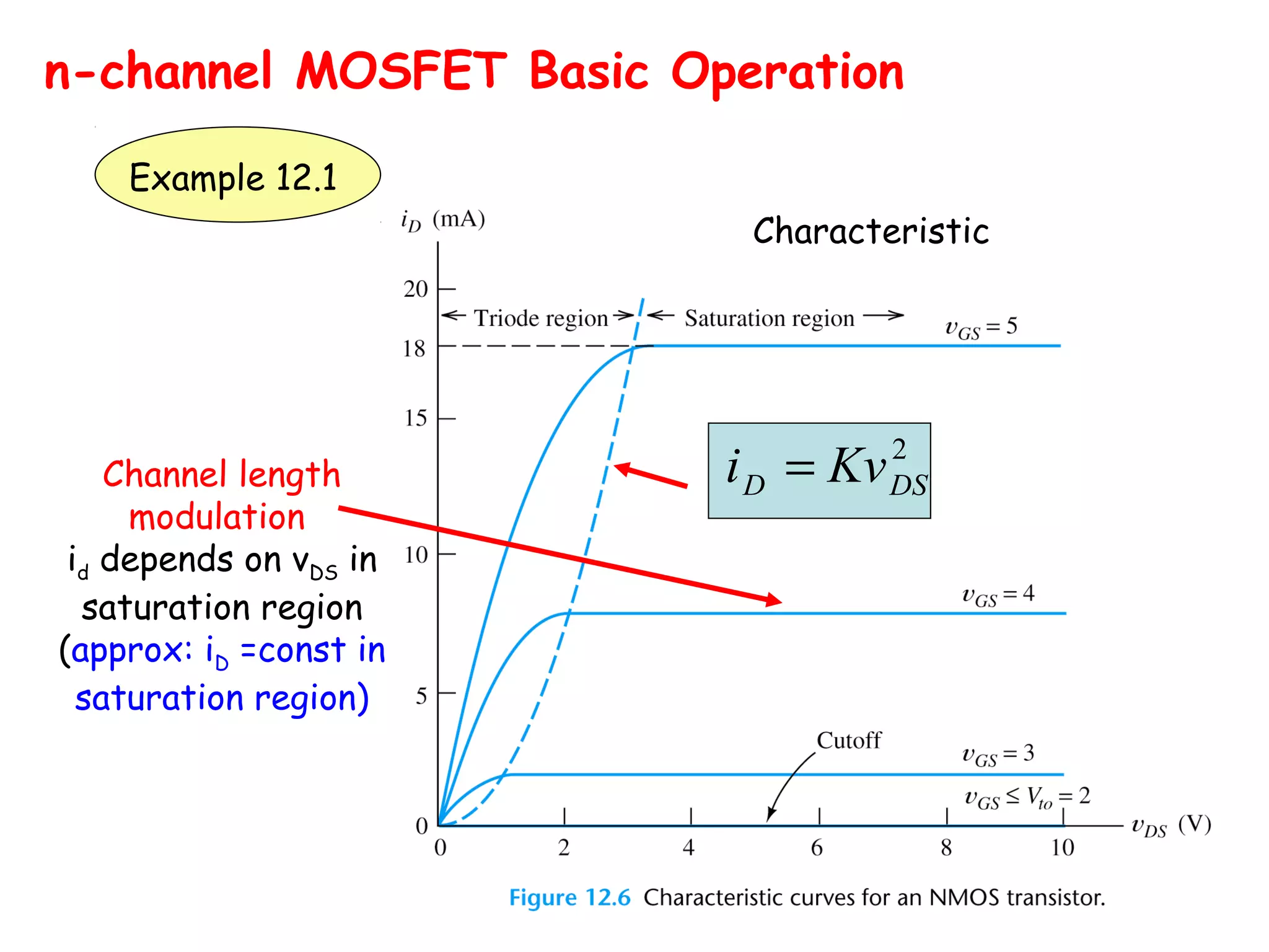
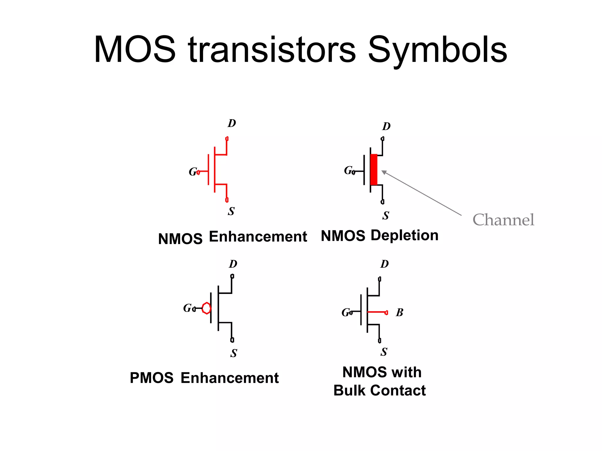
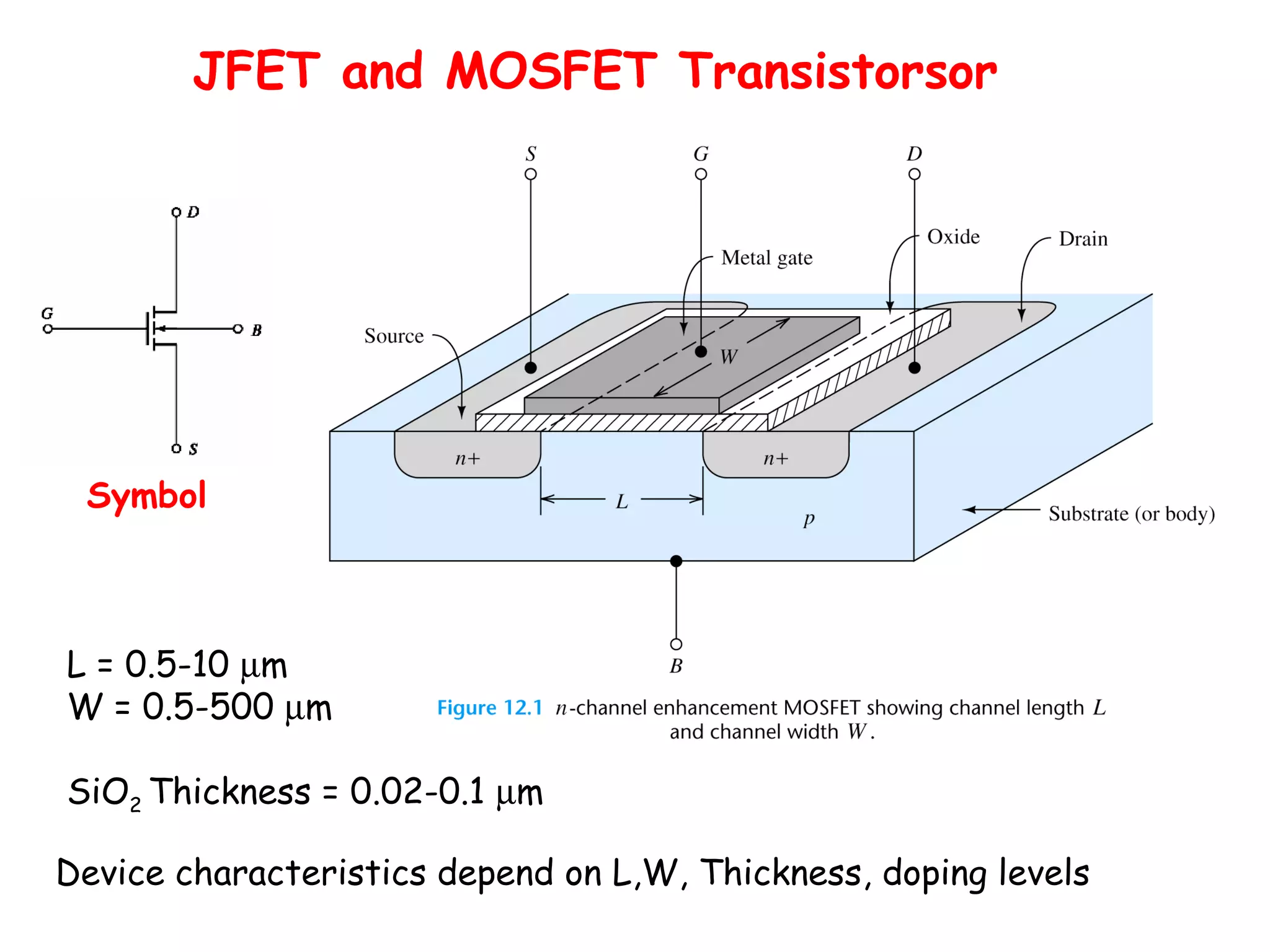
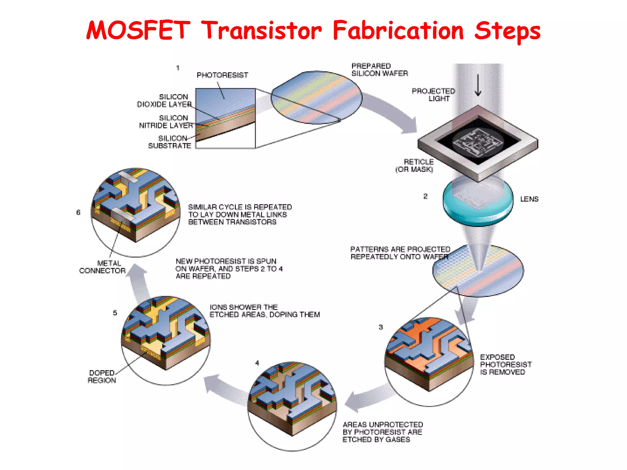
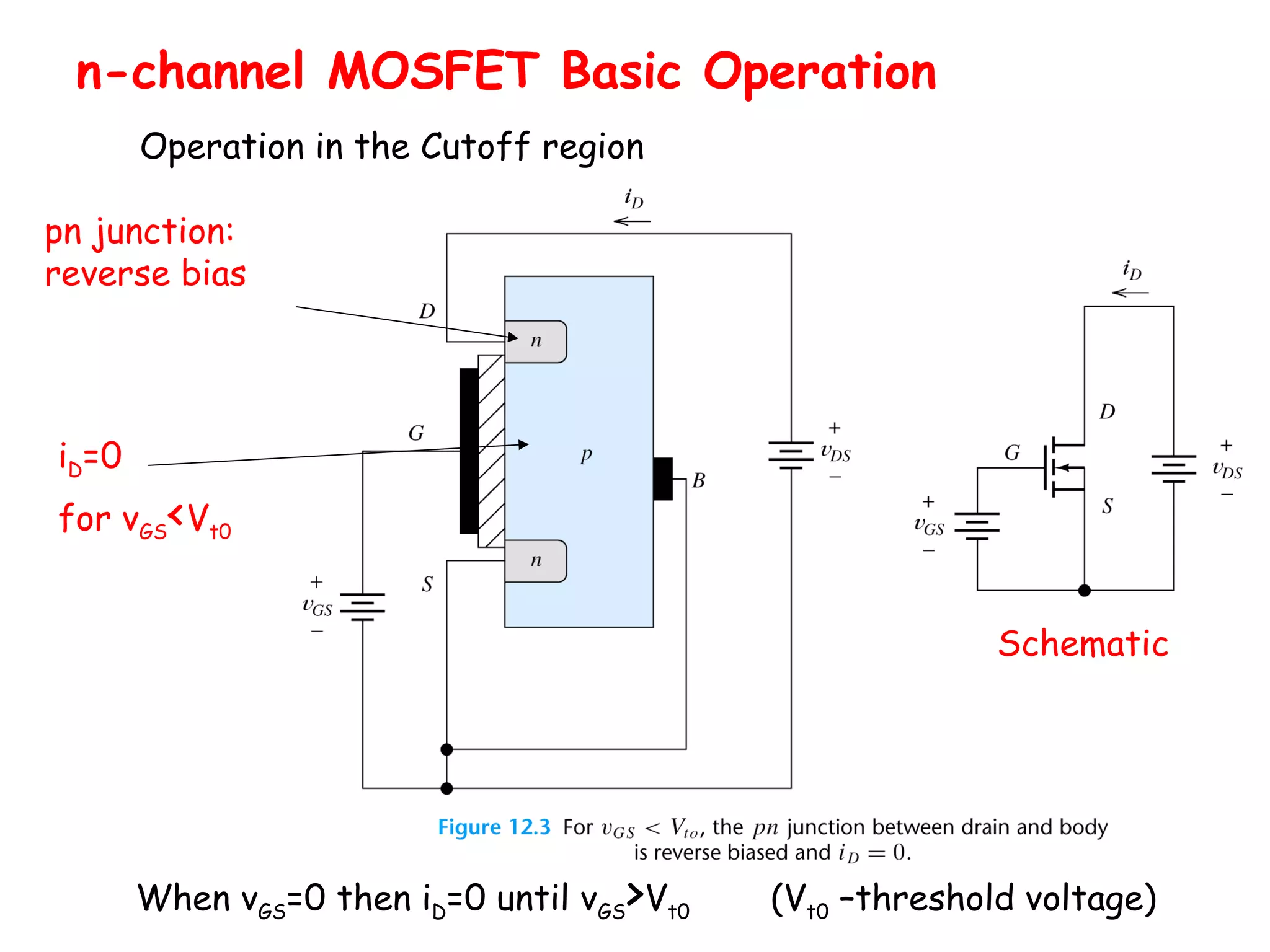
The document provides an in-depth overview of MOSFET transistors, including their construction, types (NMOS and PMOS), and basic operation principles. It details the characteristics and operational regions (cutoff, triode, and saturation) of NMOS and PMOS, as well as the factors affecting their performance. Additionally, the text includes graphical representations and schematic diagrams to illustrate the concepts discussed.


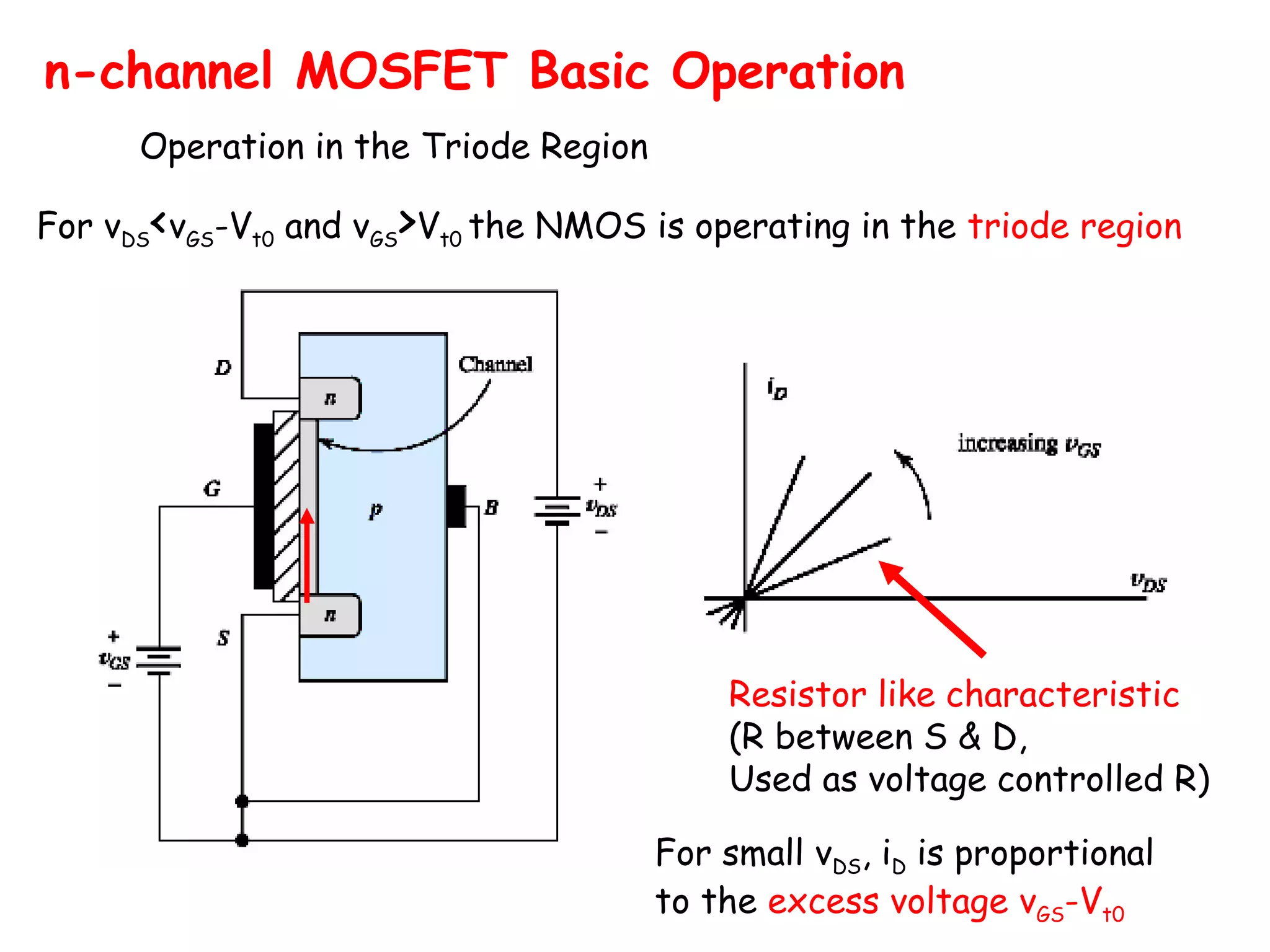
![n-channel MOSFET Basic Operation
Operation in the Triode Region
( )[ ]2
02 DSDStGSD vvVvKi −−=
2
KP
L
W
K
=
Device parameter KP for
NMOSFET is 50 µA/V2](https://image.slidesharecdn.com/transistor-181121112402/75/Transistor-12-2048.jpg)