Download to read offline
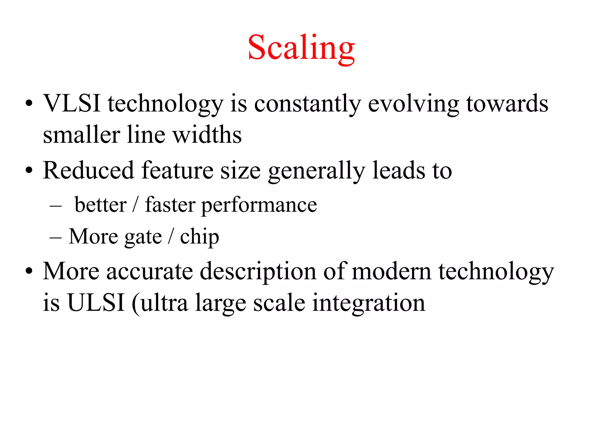
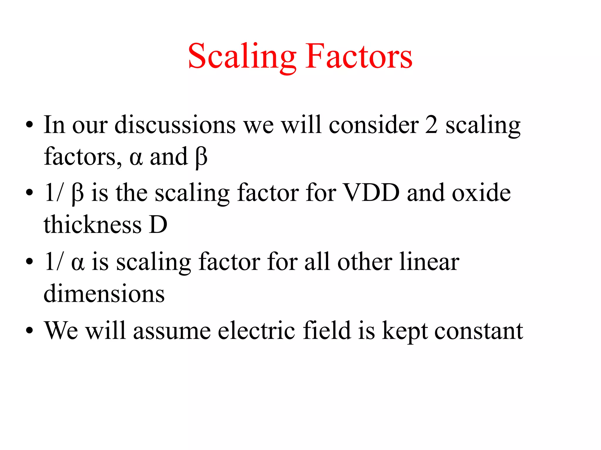
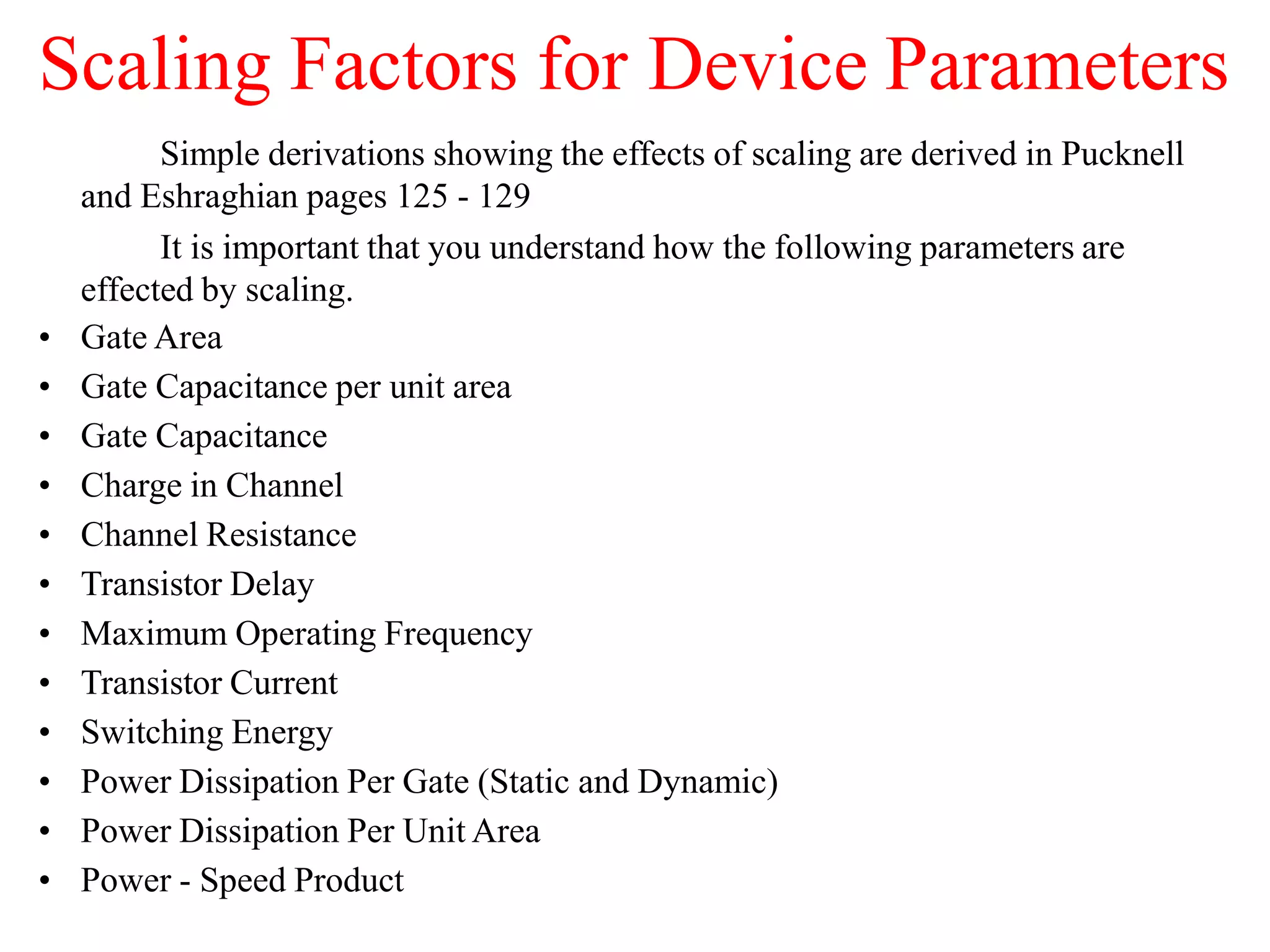
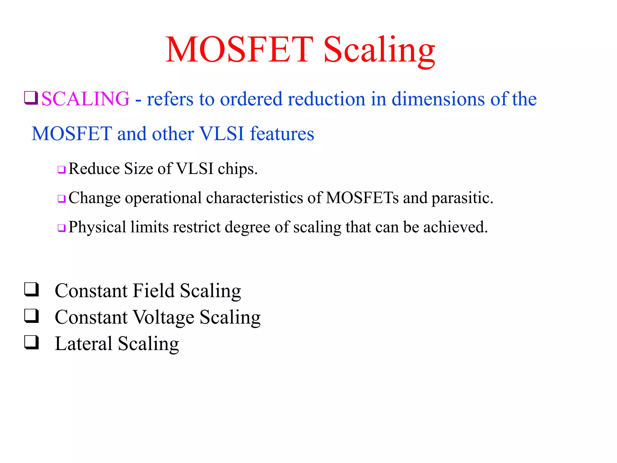
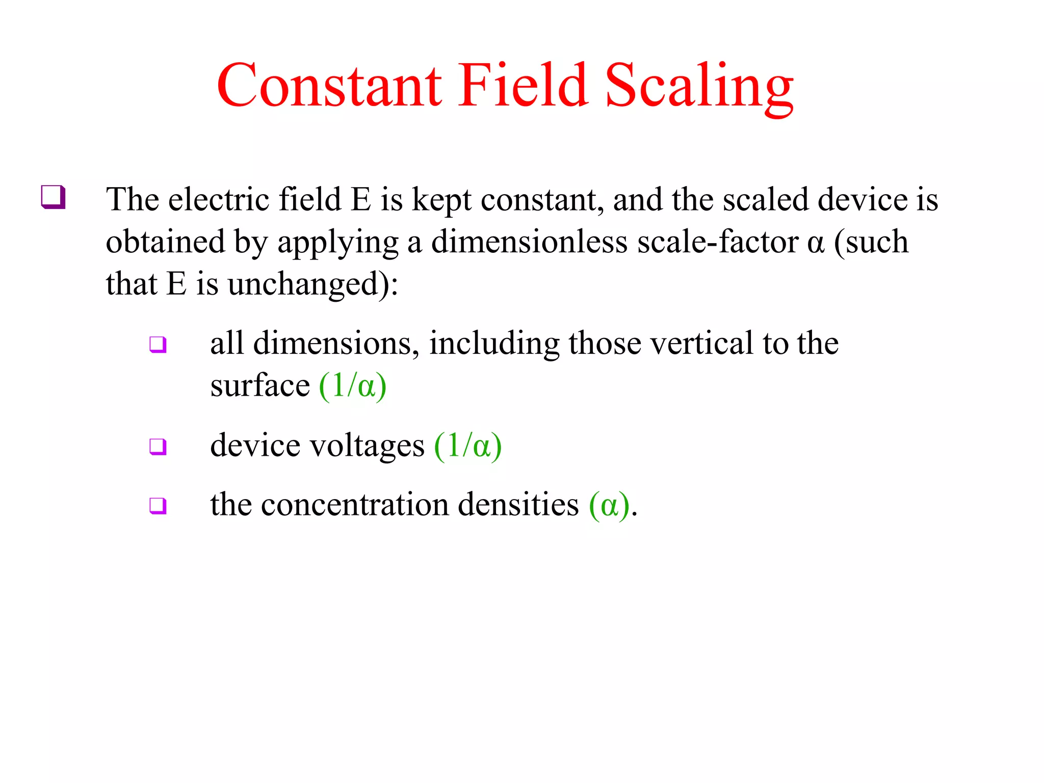
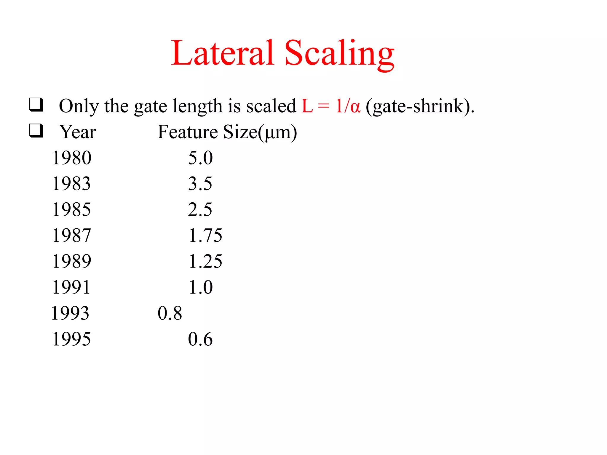
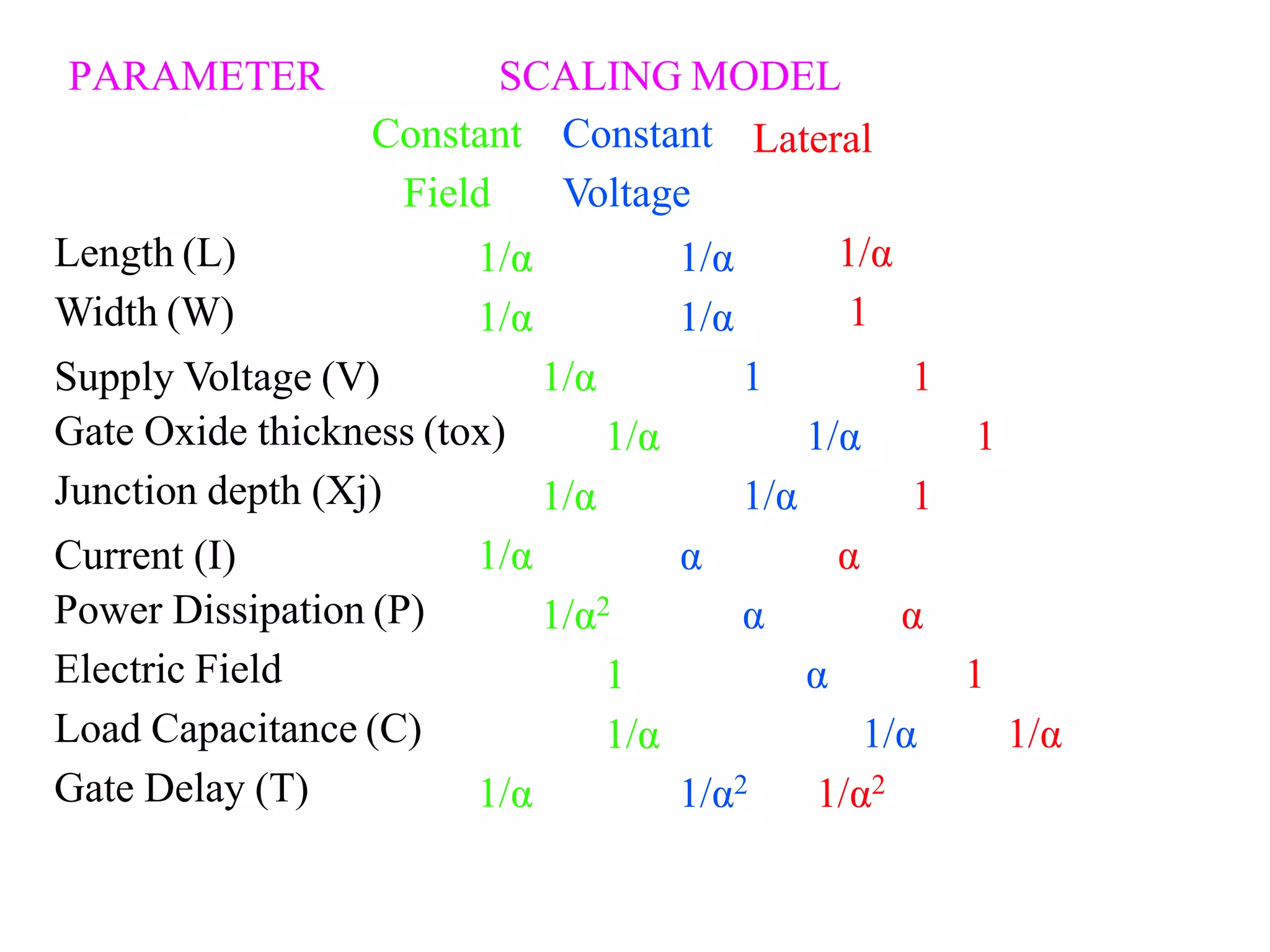
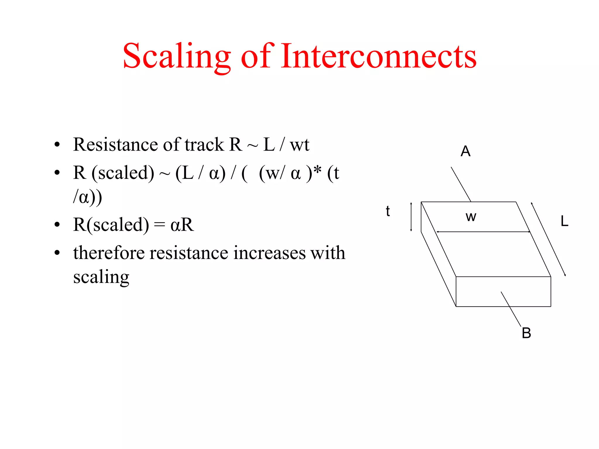


VLSI technology is constantly scaling to smaller feature sizes, known as scaling. There are two main scaling factors - α which scales all linear dimensions except oxide thickness and voltage, and β which scales oxide thickness and voltage. As devices scale, their parameters like gate area, capacitance, resistance, and delay are affected. Constant field scaling keeps the electric field constant, constant voltage keeps voltage constant, and lateral scaling only reduces the gate length. Scaling improves performance and integration density but physical limits restrict how far it can go, and it increases issues like interconnect delay and crosstalk.