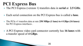
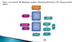
SlideShare a Scribd company logo
By:Murtadha S. Al-Sabbagh
Supervised By: Dr. Basim Abd Al-Baqi
 A bus connects all the internal computer components to the
CPU and Main memory.
 In this presentation we will present the ISA (industry standard
architecture) bus, the PCI (peripheral component interconnect)
and PCI Express buses, the USB (universal serial bus), and the
AGP (advanced graphics port).
 Also provided are some simple interfaces to many of these bus
systems as design guides.
2
 The Industry Standard Architecture, bus has been around since start of the
IBM-PC
◦ circa 1982
 Any card from the very first personal computer will plug in & function in any
P 4-desabmetsys.
◦ provided they have an ISA slot
 ISA bus mostly gone from the home PC, but still found in many industrial
applications.
◦ due to low cost & number of existing cards
4
 An ISA bus, or data pathway, operates at 8 MHz clock rate and has a
maximum data rate of 8 MBps for 8-bit bus.
 Over years, the ISA bus evolved from original 8-bit, to the
16-bit standard found today.
 With the P4, ISA bus started to disappear.
◦ a 32-bit version called the EISA bus (Extended ISA) has also
largely disappeared
5
 Fig 15–1 shows an 8-bit ISA connector as found
on the main board of all PC systems
◦ may be combined with a 16-bit connector
 The ISA bus connector contains
◦ the demultiplexed address bus (A19–A0) for
the 1M-byte 8088 system
◦ the 8-bit data bus (D7–D0)
◦ control signals MEMR, MEMW, IOR, and
IOW for controlling I/O and any memory
placed on the printed circuit card
7
 Memory is seldom added to ISA today
because ISA cards operate at only 8 MHz.
◦ EPROM or flash memory for setup may be
on some ISA cards, but never RAM
 Other signals, useful for I/O interface, are
the interrupt request lines IRQ2–IRQ7.
 DMA channel 0–3 control signals are also
present on the connector.
 IRQ2 is redirected to IRQ9 on modern
systems, and is so labeled here
8
 DMA request inputs are labeled DRQ1–DRQ3
and the DMA acknowledge outputs are labeled
DACK0 - DACK3.
 Note the DRQ0 input pin is missing,
 Early PCs used DRQ0 & the DACK0 output as a
refresh signal to refresh DRAM on the ISA card
 today, this output pin contains a 15.2 µs clock
signal used for refreshing DRAM
 remaining pins are for power and RESET
9
 Fig 15–2 shows an interface for the ISA bus, which
provides 32 bits of parallel data .
◦ this example system shows some important points about any
system interface
 It is extremely important that loading to the bus be kept to
one low-power load.
◦ a 74LS244 buffer reduces loading on the bus
 If all bus cards were to present heavy loads, the system
would not operate properly.
◦ perhaps not at all
10
11
 In the PC, the ISA bus is designed to operate at I/O address
0000H through 03FFH.
 Newer systems often allow ISA ports above 03FFH, but
older systems do not.
◦ some older cards only decode 0000H–03FFH
& may conflict with addresses above 03FFH
 The ports in 15–2 are decoded by three 74LS138 decoders.
◦ more efficient and cost-effective to decode the ports with a
programmable logic device.
13
 Figure 15–4 shows an input interface to the ISA bus, using
a pair of ADC804 analog-to-digital converters .
◦ made through a nine-pin DB9 connector
 Decoding I/O port addresses is more complex, as each
converter needs:
1. write pulse to start a conversion.
2. read pulse to read the digital data converted.
3. pulse to enable the selection of the INTRtuptuo .
14
15
 The difference between 8- & 16-bit ISA is an extra
connector behind the 8-bit connector.
 A 16-bit card contains two edge connectors:
◦ one plugs into the original 8-bit connector
◦ the other plugs into the new 16-bit connector
 Figure 15–5 shows pin-out and placement
of the additional connector in relation to the 8-bit connector.
17
18
Original 8 bit ISA
connectors
Additional
connections converts
to 16 bit ISA
 PCI (peripheral component interconnect)
is virtually the only bus found in new systems.
 PCI has replaced the ISA local bus.
 PCI has plug-and-play characteristics and
ability to function with a 64-bit data bus.
 It operates at clock speeds of 33 or 66 MHz.
 At 32 bits and 33 MHz, a PCI bus has a maximum data rate of
132 MBps.
20
 PCI functions with a 32-bit or 64-tib data bus
and a full 32-tibsserddasub.
◦ address and data buses, labeled AD 0– AD63 are multiplexed to
reduce size of the edge connector
 A 32-tibdracsahsnoitcennoc1 through 62eht ,64-tibdrac
sahlla94 connections .
 The 64-tibdracnacetadommoccaa64-tibsserddafi
deriuqertaemoserutuftniop.
22
23
 The PCI address appears on
AD 0– AD31 and
is multiplexed with data .
◦ some systems have a 64-atad tib
subgnisu
AD 32– AD63 for data transfer only
◦ these pins can be used for
extending the
address to 64 bits
24
 Frame# : is driven by the current
master to indicate the beginning of
an access and will remain active
until the final data cycle (here
DMA is not used instead some bus
arbitration scheme is).
 BC/BE#: Bus Command/Byte
Enables are multiplexed. During the
address phase of a transaction, they
define the bus command. During the
data phase, they are used as byte
enables.
PCI Commands
• PCI commands are controlled by
using the four pins C/BE3-C/BE0.
• These commands are set by CPU
to control the PCI devices.
 Special Cycle The special cycle is used to transfer
data to all PCI components. If the rightmost 16 bits
of the data bus contain a 0000H, indicating a
processor shutdown, 0001H for a processor halt, or
0002H for 80X86 specific code or data.
 Configuration Read Configuration information is
read from the PCI device .
 Configuration Write The configuration write
allows data to be written to the configuration.
 Memory Multiple This is similar to the memory
read access, except it access many data instead of
one.
 Dual Addressing Used for transferring address
information to a 64-bit PCI device. which only
contains a 32-bit data path.
 Line Memory Addressing Used to read more than
two 32-bit numbers from the PCI bus.
26
 PCI contains a 256-byte memory to allow the PC to interrogate
the PCI interface.
◦ this feature allows the system to automatically configure itself for the PCI
plug-board
◦ Microsoft calls this plug-and-play (PnP)
 The first 64 bytes contain information about the PCI interface.
 The first 32-bit doubleword contains the unit ID code and the
vendor ID code.
 Fig15–9 shows the configuration memory.
27
28
 Unit ID code is a 16-tibrebmunD31– D16.
◦ a number between 0000H & FFFEH to identify the
unit if it is installed
◦ FFFFH if the unit is not installed
 The class code is found in bits D 31– D16 of configuration
memory at location 08H .
◦ class codes identify the PCI interface class
◦ bits D 15– D0 are defined by the manufacturer
 Current class codes are listed in Table 15–5 and are
assigned by the PCI SIG.
29
 The base address space consists of a base address
for the memory, a second for the I/O space, and a
third for the expansion ROM .
 Though Intel microprocessors use a 16-O/I tib
sserdda,erehtsimoorrofgnidnapxeot32 bits
addressing.
 The status word is loaded in bits D 31– D16 of
location 04H of the configuration memory.
 the command is at bits D 15– D0 of 04H
 Fig 15–10 shows the status & command registers.
31
32
 Most modern PCs have an extension to the normal system
BIOS that supports PCI bus .
◦ these systems access PCI at interrupt vector 1AH
 Table 15–6 lists functions available through the DOS INT
1AH instruction with AH = 0B1H for the PCI.
 Example 15–5 shows how the BIOS is used
to determine whether the PCI bus extension available .
33
 The PCI Express (version 1) transfers data in serial at 2.5 GHz.
 Each serial connection on the PCI Express bus is called a lane.
 The PCIe v1 transfers data at rate 250 MBps (1 lane) to 4 GBps (16 lanes)
for PCI Express interfaces .
 A PCI Express video card connector currently has 16 lanes with
a transfer speed of 4 GBps.
35
 the lane is constructed from a pair of data pipes eno ,
atad tuptuo rof eno dna atad tupni rof
 signaling on the PCI Express bus uses 3.3 V
with differential signals
 the pin-out for the single lane connector ,
appears in Table 15–7
36
PCIe Versions Speed Comparison
Transfer rate is expressed in transfers per second instead of bits per
second because the number of transfers includes the overhead bits, which
do not provide additional throughput; PCIe 1.x uses an 8b/10b
encoding scheme, resulting in a 20% (= 2/10) overhead on the raw
channel bandwidth
 The standard allows up to 32 lanes.
◦ at present the widest is the 16 lanes video card
 Most main boards contain four single lane slots for
peripherals and one 16 lane slot for the video card.
◦ a few newer boards contain two 16 lane slots
 PCI Express 2 bus was released in late 2007.
◦ transfer speed from 250 MBps to 500 MBps,
twice that of the PCI Express v1
 PCI is replacing most current video cards on the AGP port
with the PCI Express bus.
39
 This technology allows manufacturers to use less space on
the main board and reduce the cost of manufacturing a main
board .
◦ connectors are smaller, which also reduces cost
 Software used with PCI Express remains the same as used
with the PCI bus.
◦ new programs are not needed to develop drivers
40
 The parallel printer interface (LPT) is located on the rear of
the PC.
 LPT stands for line printer.
 The printer interface gives the user access
to eight lines that can be programmed to receive or send
parallel data.
41
– the Centronics interface on the
parallel port uses two connectors
– a 25-D nip-epyteht nokcabfo
CP eht
– a 36-nipscinortneCeht nokcab
eht foretnirp
– the pin-outs of these connectors
are listed in
Table 15–8
42
 The parallel port can work as both a receiver and a
transmitter at its data pins D 0– D7
◦ allows other devices such as CD-ROMs, to be connected to and
used by the PC through port
 Anything that can receive and/or send data through an 8-
tibecafretninacdnanetfoseodtcennocotehtlellaraptrop
TPL(1CP a fo ).
 See Figure 15–14.
44
 The data port 378H
 The status register 379H
 An additional status port
37AH
 Note that some of
the status bits are true when
logic 0
Shown here are the contents
of:
45
 For most systems since the PS/2, one can follow the
information presented in Fig 15–14 to use the parallel port.
 To read the port, it must be initialized by sending 20H to
register 37AH.
 Once the parallel port is programmed to function as an input
port, reading is accomplished by accessing the data port at
address 378H.
 To write data to the parallel port, reprogram the command
register at address 37A by writing 00H to program the
bidirectional bit with a zero. data are then sent to the parallel
port through the data port at address 378H.
46
 On 80286 systems, the bidirectional bit is missing from the
interface.
◦ these systems do not have a register at 37AH
◦ to read information from the parallel port, write 0FFH to the port
(378H), so that it can be read
 Accessing the printer port from Windows is difficult
because a driver must be written for Windows 2000 or
Windows XP.
 Windows 98 or Windows ME port access
is accomplished as explained for DOS.
47
 Serial communications ports are COM1–COM8
◦ most PCs have only COM1 and COM2 installed
 Under DOS these ports are controlled and accessed with the
16550 serial interface.
 USB devices often interface using the HID (human
interface device) as a COM port.
◦ allows standard serial software to access USB
48
 The universal serial bus (USB) has solved a problem with the PC system.
 Current PCI sound cards use internal PC power, which generates a lot of
noise.
◦ USB allows the sound card to have its own power supply, for high-fidelity sound with no
60 Hz hum
 Other benefits are ease of connection and access to up to 127 different
connections.
 The interface is ideal for keyboards, sound cards, simple video-retrieval, and
modems.
50
 USB Types Comparison (Power & Data rate):
51
The Connector
– two types of connectors are specified, both are in
use
– there are four pins on each connector, with signals
indicated in Table 15–10
– the +5.0 V and ground can power devices
connected to the bus
– data signals are biphase signals
– when +data are at 5.0 V, –data are at zero volts and
vice versa
52
 Data signals are biphase signals generated using a circuit such as
shown in Fig 15–16.
 The line receiver is also shown.
 A noise-suppression circuit available from Texas Instruments
(SN75240) is placed on the transmission pair
 Once the transceiver is in place, interfacing
to the USB is complete.
53
– a 75773 IC from Texas Instruments functions as
differential line driver and receiver here
54
– USB uses NRZI (non-return to zero, inverted)
encoding to transmit packet data
– this method does not change signal level for
the transmission of logic 1
– signal level is inverted for each change to logic 0
55
 Actual data transmitted includes sync bits, a method called
bit stuffing, because it lengthens the data stream.
 If logic 1 is transmitted for more than 6 bits in a row, the bit
stuffing technique adds an extra bit (logic 0) after six
continuous 1s in a row.
 Bit stuffing ensures the receiver can maintain
synchronization for long strings of 1s.
◦ data are always transmitted with the least-significant bit first,
followed by subsequent bits
 See Fig 15–18.
56
– a bit-stuffed serial data stream
and the algorithm used to create
it from raw digital serial data
57
58
 To begin communication, sync byte 80H is transmitted first, followed by the
packet identification byte (PID).
 The PID contains 8 bits.
◦ only the rightmost 4 bits contain the type of packet that follows, if any.
 The leftmost 4 bits of the PID are the ones complementing the rightmost 4
bits.
 ENDP (endpoint) is a 4-tibrebmundesuybBSU eht.
◦ Endpoint 0000 is used for initialization .
◦ Other endpoints are unique to each USB device.
59
 Two types of CRC (cyclic redundancy checks )desuno
BSU.
◦ 5-bit CRC generated with polynomial X 5X +2+1
◦ a 16-,CRC tibdesuatad rofstekcap,detarenegX eht htiw16X +15
X +2+1 polynomial
 When using 5-a ,CRC tiblaudiserfo01100 is received for
no error in all five bits of the CRC and the data bits .
◦ a 16-tibonrorreCRClaudisersi1000000000001101
60
 Once a packet is transferred from host to USB device, if
data & CRC are received correctly, ACK (acknowledge) is
sent to the host .
 If data and CRC are not devieceryltcerroc( KAN eht ,ton
egdelwonkcasi )tnes.
◦ if the host receives a NAK token, it retransmits
the data packet until it is received correctly
 This method of data transfer is often called stop and wait
flow control .
◦ host must wait for client to send an ACK or
NAK before transferring additional data packets
61
 National Semiconductor produces a USB bus interface
easy to interface to the processor.
 Connect this device using non-DMA access:
◦ connect the data bus to D0–D7
◦ connect control inputs RD, WR, and CS and a 24 MHz fundamental
crystal across XIn and XOut pins
 The USB bus connection is located on the D– and D+ pins.
 Figure 15–20 shows a USBN9604 USB node.
62
 USBN9604 is a USB
bus transceiver that can
receive and transmit
USB data
 this provides an interface
point to
the USB bus for
a minimal cost of about
two dollars
63
 Simplest interface is achieved by connecting the two mode
inputs to ground .
 This places the device into nonmultiplexed parallel mode .
◦ in this mode the A0 pin is used to select address ( 1(roatad (0)
 Fig 15–21 shows this connection decodes
at I/O addresses 0300H (data) and 0301H (address)
64
65
 The latest addition to most systems was the accelerated
graphics port (AGP), until PCI Express became available
for video.
 It is designed for transfer between video card and system
memory at a maximum speed.
◦ AGP transfers at a maximum of 2GB/s
67
68
Thank you ^_~

More Related Content

What's hot

8086 pin details
8086 pin details8086 pin details
8086 pin details
AJAL A J
 
Addressing modes of 80386
Addressing modes of 80386Addressing modes of 80386
Addressing modes of 80386
PDFSHARE
 
8085 Paper Presentation slides,ppt,microprocessor 8085 ,guide, instruction set
8085 Paper Presentation slides,ppt,microprocessor 8085 ,guide, instruction set8085 Paper Presentation slides,ppt,microprocessor 8085 ,guide, instruction set
8085 Paper Presentation slides,ppt,microprocessor 8085 ,guide, instruction set
Saumitra Rukmangad
 
8051 Microcontroller PPT's By Er. Swapnil Kaware
8051 Microcontroller PPT's By Er. Swapnil Kaware8051 Microcontroller PPT's By Er. Swapnil Kaware
8051 Microcontroller PPT's By Er. Swapnil KawareProf. Swapnil V. Kaware
 
Embedded firmware
Embedded firmwareEmbedded firmware
Embedded firmware
Joel P
 
8085 microprocessor ramesh gaonkar
8085 microprocessor   ramesh gaonkar8085 microprocessor   ramesh gaonkar
8085 microprocessor ramesh gaonkar
SAQUIB AHMAD
 
Architecture of 80286 microprocessor
Architecture of 80286 microprocessorArchitecture of 80286 microprocessor
Architecture of 80286 microprocessor
Syed Ahmed Zaki
 
Microprocessor architecture-I
Microprocessor architecture-IMicroprocessor architecture-I
Microprocessor architecture-I
Dr.YNM
 
Address decoding (1).pptx
Address decoding (1).pptxAddress decoding (1).pptx
Address decoding (1).pptx
OhenebaAsamoah
 
8155 PPI
8155 PPI8155 PPI
8155 PPI
ShivamSood22
 
Memory organization of 8051
Memory organization of 8051Memory organization of 8051
Memory organization of 8051Muthu Manickam
 
Memory banking-of-8086-final
Memory banking-of-8086-finalMemory banking-of-8086-final
Memory banking-of-8086-final
Estiak Khan
 
Memory Organization
Memory OrganizationMemory Organization
Memory Organization
Acad
 
Microprocessor
MicroprocessorMicroprocessor
Microprocessor
Anand Tiwari
 
8051 Addressing Modes
8051 Addressing Modes8051 Addressing Modes
8051 Addressing Modes
Senthil Kumar
 
8085 MICROPROCESSOR
8085 MICROPROCESSOR 8085 MICROPROCESSOR
8085 MICROPROCESSOR
THANDAIAH PRABU
 
Case Study of Embedded Systems
Case Study of Embedded SystemsCase Study of Embedded Systems
Case Study of Embedded Systems
anand hd
 
Intel 8051 - pin description
Intel 8051  - pin descriptionIntel 8051  - pin description
Intel 8051 - pin description
DEPARTMENT OF PHYSICS
 
L8 understanding-atmega328 p-1
L8 understanding-atmega328 p-1L8 understanding-atmega328 p-1
L8 understanding-atmega328 p-1
rsamurti
 
Addressing modes of 8051
Addressing modes of 8051Addressing modes of 8051
Addressing modes of 8051
SARITHA REDDY
 

What's hot (20)

8086 pin details
8086 pin details8086 pin details
8086 pin details
 
Addressing modes of 80386
Addressing modes of 80386Addressing modes of 80386
Addressing modes of 80386
 
8085 Paper Presentation slides,ppt,microprocessor 8085 ,guide, instruction set
8085 Paper Presentation slides,ppt,microprocessor 8085 ,guide, instruction set8085 Paper Presentation slides,ppt,microprocessor 8085 ,guide, instruction set
8085 Paper Presentation slides,ppt,microprocessor 8085 ,guide, instruction set
 
8051 Microcontroller PPT's By Er. Swapnil Kaware
8051 Microcontroller PPT's By Er. Swapnil Kaware8051 Microcontroller PPT's By Er. Swapnil Kaware
8051 Microcontroller PPT's By Er. Swapnil Kaware
 
Embedded firmware
Embedded firmwareEmbedded firmware
Embedded firmware
 
8085 microprocessor ramesh gaonkar
8085 microprocessor   ramesh gaonkar8085 microprocessor   ramesh gaonkar
8085 microprocessor ramesh gaonkar
 
Architecture of 80286 microprocessor
Architecture of 80286 microprocessorArchitecture of 80286 microprocessor
Architecture of 80286 microprocessor
 
Microprocessor architecture-I
Microprocessor architecture-IMicroprocessor architecture-I
Microprocessor architecture-I
 
Address decoding (1).pptx
Address decoding (1).pptxAddress decoding (1).pptx
Address decoding (1).pptx
 
8155 PPI
8155 PPI8155 PPI
8155 PPI
 
Memory organization of 8051
Memory organization of 8051Memory organization of 8051
Memory organization of 8051
 
Memory banking-of-8086-final
Memory banking-of-8086-finalMemory banking-of-8086-final
Memory banking-of-8086-final
 
Memory Organization
Memory OrganizationMemory Organization
Memory Organization
 
Microprocessor
MicroprocessorMicroprocessor
Microprocessor
 
8051 Addressing Modes
8051 Addressing Modes8051 Addressing Modes
8051 Addressing Modes
 
8085 MICROPROCESSOR
8085 MICROPROCESSOR 8085 MICROPROCESSOR
8085 MICROPROCESSOR
 
Case Study of Embedded Systems
Case Study of Embedded SystemsCase Study of Embedded Systems
Case Study of Embedded Systems
 
Intel 8051 - pin description
Intel 8051  - pin descriptionIntel 8051  - pin description
Intel 8051 - pin description
 
L8 understanding-atmega328 p-1
L8 understanding-atmega328 p-1L8 understanding-atmega328 p-1
L8 understanding-atmega328 p-1
 
Addressing modes of 8051
Addressing modes of 8051Addressing modes of 8051
Addressing modes of 8051
 

Viewers also liked

Bus interface 8086
Bus interface 8086Bus interface 8086
Bus interface 8086
University of Gujrat, Pakistan
 
Isa Dma & Bus Masters
Isa Dma & Bus MastersIsa Dma & Bus Masters
Isa Dma & Bus Masters
nishantshah2381
 
Programed I/O Modul..
Programed I/O Modul..Programed I/O Modul..
Programed I/O Modul..
Myster Rius
 
Advanced computer architect lesson 3 and 4
Advanced computer architect lesson 3 and 4Advanced computer architect lesson 3 and 4
Advanced computer architect lesson 3 and 4
Ismail Mukiibi
 
Architecture of 8086
Architecture of 8086Architecture of 8086
Architecture of 8086Nikhil Kumar
 
8086 ppt
8086 ppt8086 ppt
8086 ppt
raju kusale
 
13. peripheral component interconnect (pci)
13. peripheral component interconnect (pci)13. peripheral component interconnect (pci)
13. peripheral component interconnect (pci)
Rumah Belajar
 
Pin Description Of Intel 80386 DX Microprocessor
Pin Description Of Intel 80386 DX MicroprocessorPin Description Of Intel 80386 DX Microprocessor
Pin Description Of Intel 80386 DX Microprocessor
Raunaq Sahni
 
Design of FPGA based 8-bit RISC Controller IP core using VHDL
Design of FPGA based 8-bit RISC Controller IP core using VHDLDesign of FPGA based 8-bit RISC Controller IP core using VHDL
Design of FPGA based 8-bit RISC Controller IP core using VHDL
Aneesh Raveendran
 
Design and Implementation of an Advanced DMA Controller on AMBA-Based SoC
Design and Implementation of an Advanced DMA Controller on AMBA-Based SoCDesign and Implementation of an Advanced DMA Controller on AMBA-Based SoC
Design and Implementation of an Advanced DMA Controller on AMBA-Based SoC
Rabindranath Tagore University, Bhopal
 
Microchip's PIC Micro Controller
Microchip's PIC Micro ControllerMicrochip's PIC Micro Controller
Microchip's PIC Micro Controller
Midhu S V Unnithan
 
Arm corrected ppt
Arm corrected pptArm corrected ppt
Arm corrected ppt
anish jagan
 
8051 io interface
8051 io interface8051 io interface
8051 io interface
Abhinav Shubham
 
8085 interfacing with memory chips
8085 interfacing with memory chips8085 interfacing with memory chips
8085 interfacing with memory chips
Srikrishna Thota
 
Minimum Modes and Maximum Modes of 8086 Microprocessor
Minimum Modes and Maximum Modes of 8086 MicroprocessorMinimum Modes and Maximum Modes of 8086 Microprocessor
Minimum Modes and Maximum Modes of 8086 MicroprocessorNikhil Kumar
 
Direct Memory Access
Direct Memory AccessDirect Memory Access
Direct Memory Access
Sanjay Saluth
 
Real Time Systems & RTOS
Real Time Systems & RTOSReal Time Systems & RTOS
Real Time Systems & RTOS
Vishwa Mohan
 

Viewers also liked (20)

Bus interface 8086
Bus interface 8086Bus interface 8086
Bus interface 8086
 
Isa Dma & Bus Masters
Isa Dma & Bus MastersIsa Dma & Bus Masters
Isa Dma & Bus Masters
 
Programed I/O Modul..
Programed I/O Modul..Programed I/O Modul..
Programed I/O Modul..
 
Advanced computer architect lesson 3 and 4
Advanced computer architect lesson 3 and 4Advanced computer architect lesson 3 and 4
Advanced computer architect lesson 3 and 4
 
Architecture of 8086
Architecture of 8086Architecture of 8086
Architecture of 8086
 
8086 ppt
8086 ppt8086 ppt
8086 ppt
 
13. peripheral component interconnect (pci)
13. peripheral component interconnect (pci)13. peripheral component interconnect (pci)
13. peripheral component interconnect (pci)
 
Pin Description Of Intel 80386 DX Microprocessor
Pin Description Of Intel 80386 DX MicroprocessorPin Description Of Intel 80386 DX Microprocessor
Pin Description Of Intel 80386 DX Microprocessor
 
Design of FPGA based 8-bit RISC Controller IP core using VHDL
Design of FPGA based 8-bit RISC Controller IP core using VHDLDesign of FPGA based 8-bit RISC Controller IP core using VHDL
Design of FPGA based 8-bit RISC Controller IP core using VHDL
 
A tmega8 basics
A tmega8 basicsA tmega8 basics
A tmega8 basics
 
Design and Implementation of an Advanced DMA Controller on AMBA-Based SoC
Design and Implementation of an Advanced DMA Controller on AMBA-Based SoCDesign and Implementation of an Advanced DMA Controller on AMBA-Based SoC
Design and Implementation of an Advanced DMA Controller on AMBA-Based SoC
 
Microchip's PIC Micro Controller
Microchip's PIC Micro ControllerMicrochip's PIC Micro Controller
Microchip's PIC Micro Controller
 
Arm corrected ppt
Arm corrected pptArm corrected ppt
Arm corrected ppt
 
8051 io interface
8051 io interface8051 io interface
8051 io interface
 
8085 interfacing with memory chips
8085 interfacing with memory chips8085 interfacing with memory chips
8085 interfacing with memory chips
 
Microprocessors 1-8086
Microprocessors 1-8086Microprocessors 1-8086
Microprocessors 1-8086
 
Minimum Modes and Maximum Modes of 8086 Microprocessor
Minimum Modes and Maximum Modes of 8086 MicroprocessorMinimum Modes and Maximum Modes of 8086 Microprocessor
Minimum Modes and Maximum Modes of 8086 Microprocessor
 
Direct Memory Access
Direct Memory AccessDirect Memory Access
Direct Memory Access
 
Real Time Systems & RTOS
Real Time Systems & RTOSReal Time Systems & RTOS
Real Time Systems & RTOS
 
DMA presentation [By- Digvijay]
DMA presentation [By- Digvijay]DMA presentation [By- Digvijay]
DMA presentation [By- Digvijay]
 

Similar to Bus Interfacing with Intel Microprocessors Based Systems

Bus
BusBus
Pc interface
Pc interfacePc interface
Pc interface
Ashraf Aboshosha
 
Pcie basic
Pcie basicPcie basic
Pcie basic
Saifuddin Kaijar
 
Cpi unit 01
Cpi unit 01Cpi unit 01
Cpi unit 01
Gurpreet Singh
 
Mother board
Mother boardMother board
Mother board
Sripati Mahapatra
 
Chapter 6: Expansion Buses
Chapter 6: Expansion BusesChapter 6: Expansion Buses
Chapter 6: Expansion Busesaskme
 
PCIe and PCIe driver in WEC7 (Windows Embedded compact 7)
PCIe and PCIe driver in WEC7 (Windows Embedded compact 7)PCIe and PCIe driver in WEC7 (Windows Embedded compact 7)
PCIe and PCIe driver in WEC7 (Windows Embedded compact 7)
gnkeshava
 
Motherboard components and their functions
Motherboard components and their functionsMotherboard components and their functions
Motherboard components and their functions
Abdullah-Al- Mahmud
 
VJITSk 6713 user manual
VJITSk 6713 user manualVJITSk 6713 user manual
VJITSk 6713 user manual
kot seelam
 
Microprocessor and Application (8085)
Microprocessor and Application (8085)Microprocessor and Application (8085)
Microprocessor and Application (8085)ufaq kk
 
PCI Bridge Performance
PCI Bridge PerformancePCI Bridge Performance
PCI Bridge PerformanceMohamad Tisani
 
Bus & Interface
Bus & InterfaceBus & Interface
Bus & Interface
ImranulHasan6
 
Module 1 8086
Module 1 8086Module 1 8086
Module 1 8086
Deepak John
 
Commnunication ports and memory card chapter 1
Commnunication ports and memory card chapter 1Commnunication ports and memory card chapter 1
Commnunication ports and memory card chapter 1Mukesh Thakur
 
P C I L O C A L B U S
P C I  L O C A L  B U S P C I  L O C A L  B U S
P C I L O C A L B U S jainfu2
 
Intel 8086 microprocessor
Intel 8086 microprocessorIntel 8086 microprocessor
Intel 8086 microprocessor
Ravi Yasas
 
amba.ppt
amba.pptamba.ppt
amba.ppt
Rahul534035
 
amba.ppt
amba.pptamba.ppt
amba.ppt
DivyaDewkathe
 
amba.ppt
amba.pptamba.ppt
amba.ppt
VediAshutosh
 

Similar to Bus Interfacing with Intel Microprocessors Based Systems (20)

Bus
BusBus
Bus
 
Pc interface
Pc interfacePc interface
Pc interface
 
Chap1 expan slots
Chap1 expan slotsChap1 expan slots
Chap1 expan slots
 
Pcie basic
Pcie basicPcie basic
Pcie basic
 
Cpi unit 01
Cpi unit 01Cpi unit 01
Cpi unit 01
 
Mother board
Mother boardMother board
Mother board
 
Chapter 6: Expansion Buses
Chapter 6: Expansion BusesChapter 6: Expansion Buses
Chapter 6: Expansion Buses
 
PCIe and PCIe driver in WEC7 (Windows Embedded compact 7)
PCIe and PCIe driver in WEC7 (Windows Embedded compact 7)PCIe and PCIe driver in WEC7 (Windows Embedded compact 7)
PCIe and PCIe driver in WEC7 (Windows Embedded compact 7)
 
Motherboard components and their functions
Motherboard components and their functionsMotherboard components and their functions
Motherboard components and their functions
 
VJITSk 6713 user manual
VJITSk 6713 user manualVJITSk 6713 user manual
VJITSk 6713 user manual
 
Microprocessor and Application (8085)
Microprocessor and Application (8085)Microprocessor and Application (8085)
Microprocessor and Application (8085)
 
PCI Bridge Performance
PCI Bridge PerformancePCI Bridge Performance
PCI Bridge Performance
 
Bus & Interface
Bus & InterfaceBus & Interface
Bus & Interface
 
Module 1 8086
Module 1 8086Module 1 8086
Module 1 8086
 
Commnunication ports and memory card chapter 1
Commnunication ports and memory card chapter 1Commnunication ports and memory card chapter 1
Commnunication ports and memory card chapter 1
 
P C I L O C A L B U S
P C I  L O C A L  B U S P C I  L O C A L  B U S
P C I L O C A L B U S
 
Intel 8086 microprocessor
Intel 8086 microprocessorIntel 8086 microprocessor
Intel 8086 microprocessor
 
amba.ppt
amba.pptamba.ppt
amba.ppt
 
amba.ppt
amba.pptamba.ppt
amba.ppt
 
amba.ppt
amba.pptamba.ppt
amba.ppt
 

Recently uploaded

FIDO Alliance Osaka Seminar: Passkeys at Amazon.pdf
FIDO Alliance Osaka Seminar: Passkeys at Amazon.pdfFIDO Alliance Osaka Seminar: Passkeys at Amazon.pdf
FIDO Alliance Osaka Seminar: Passkeys at Amazon.pdf
FIDO Alliance
 
From Siloed Products to Connected Ecosystem: Building a Sustainable and Scala...
From Siloed Products to Connected Ecosystem: Building a Sustainable and Scala...From Siloed Products to Connected Ecosystem: Building a Sustainable and Scala...
From Siloed Products to Connected Ecosystem: Building a Sustainable and Scala...
Product School
 
Monitoring Java Application Security with JDK Tools and JFR Events
Monitoring Java Application Security with JDK Tools and JFR EventsMonitoring Java Application Security with JDK Tools and JFR Events
Monitoring Java Application Security with JDK Tools and JFR Events
Ana-Maria Mihalceanu
 
UiPath Test Automation using UiPath Test Suite series, part 3
UiPath Test Automation using UiPath Test Suite series, part 3UiPath Test Automation using UiPath Test Suite series, part 3
UiPath Test Automation using UiPath Test Suite series, part 3
DianaGray10
 
Builder.ai Founder Sachin Dev Duggal's Strategic Approach to Create an Innova...
Builder.ai Founder Sachin Dev Duggal's Strategic Approach to Create an Innova...Builder.ai Founder Sachin Dev Duggal's Strategic Approach to Create an Innova...
Builder.ai Founder Sachin Dev Duggal's Strategic Approach to Create an Innova...
Ramesh Iyer
 
Transcript: Selling digital books in 2024: Insights from industry leaders - T...
Transcript: Selling digital books in 2024: Insights from industry leaders - T...Transcript: Selling digital books in 2024: Insights from industry leaders - T...
Transcript: Selling digital books in 2024: Insights from industry leaders - T...
BookNet Canada
 
De-mystifying Zero to One: Design Informed Techniques for Greenfield Innovati...
De-mystifying Zero to One: Design Informed Techniques for Greenfield Innovati...De-mystifying Zero to One: Design Informed Techniques for Greenfield Innovati...
De-mystifying Zero to One: Design Informed Techniques for Greenfield Innovati...
Product School
 
Mission to Decommission: Importance of Decommissioning Products to Increase E...
Mission to Decommission: Importance of Decommissioning Products to Increase E...Mission to Decommission: Importance of Decommissioning Products to Increase E...
Mission to Decommission: Importance of Decommissioning Products to Increase E...
Product School
 
Assuring Contact Center Experiences for Your Customers With ThousandEyes
Assuring Contact Center Experiences for Your Customers With ThousandEyesAssuring Contact Center Experiences for Your Customers With ThousandEyes
Assuring Contact Center Experiences for Your Customers With ThousandEyes
ThousandEyes
 
How world-class product teams are winning in the AI era by CEO and Founder, P...
How world-class product teams are winning in the AI era by CEO and Founder, P...How world-class product teams are winning in the AI era by CEO and Founder, P...
How world-class product teams are winning in the AI era by CEO and Founder, P...
Product School
 
Slack (or Teams) Automation for Bonterra Impact Management (fka Social Soluti...
Slack (or Teams) Automation for Bonterra Impact Management (fka Social Soluti...Slack (or Teams) Automation for Bonterra Impact Management (fka Social Soluti...
Slack (or Teams) Automation for Bonterra Impact Management (fka Social Soluti...
Jeffrey Haguewood
 
When stars align: studies in data quality, knowledge graphs, and machine lear...
When stars align: studies in data quality, knowledge graphs, and machine lear...When stars align: studies in data quality, knowledge graphs, and machine lear...
When stars align: studies in data quality, knowledge graphs, and machine lear...
Elena Simperl
 
The Future of Platform Engineering
The Future of Platform EngineeringThe Future of Platform Engineering
The Future of Platform Engineering
Jemma Hussein Allen
 
DevOps and Testing slides at DASA Connect
DevOps and Testing slides at DASA ConnectDevOps and Testing slides at DASA Connect
DevOps and Testing slides at DASA Connect
Kari Kakkonen
 
Elevating Tactical DDD Patterns Through Object Calisthenics
Elevating Tactical DDD Patterns Through Object CalisthenicsElevating Tactical DDD Patterns Through Object Calisthenics
Elevating Tactical DDD Patterns Through Object Calisthenics
Dorra BARTAGUIZ
 
GDG Cloud Southlake #33: Boule & Rebala: Effective AppSec in SDLC using Deplo...
GDG Cloud Southlake #33: Boule & Rebala: Effective AppSec in SDLC using Deplo...GDG Cloud Southlake #33: Boule & Rebala: Effective AppSec in SDLC using Deplo...
GDG Cloud Southlake #33: Boule & Rebala: Effective AppSec in SDLC using Deplo...
James Anderson
 
Neuro-symbolic is not enough, we need neuro-*semantic*
Neuro-symbolic is not enough, we need neuro-*semantic*Neuro-symbolic is not enough, we need neuro-*semantic*
Neuro-symbolic is not enough, we need neuro-*semantic*
Frank van Harmelen
 
PCI PIN Basics Webinar from the Controlcase Team
PCI PIN Basics Webinar from the Controlcase TeamPCI PIN Basics Webinar from the Controlcase Team
PCI PIN Basics Webinar from the Controlcase Team
ControlCase
 
The Art of the Pitch: WordPress Relationships and Sales
The Art of the Pitch: WordPress Relationships and SalesThe Art of the Pitch: WordPress Relationships and Sales
The Art of the Pitch: WordPress Relationships and Sales
Laura Byrne
 
Generating a custom Ruby SDK for your web service or Rails API using Smithy
Generating a custom Ruby SDK for your web service or Rails API using SmithyGenerating a custom Ruby SDK for your web service or Rails API using Smithy
Generating a custom Ruby SDK for your web service or Rails API using Smithy
g2nightmarescribd
 

Recently uploaded (20)

FIDO Alliance Osaka Seminar: Passkeys at Amazon.pdf
FIDO Alliance Osaka Seminar: Passkeys at Amazon.pdfFIDO Alliance Osaka Seminar: Passkeys at Amazon.pdf
FIDO Alliance Osaka Seminar: Passkeys at Amazon.pdf
 
From Siloed Products to Connected Ecosystem: Building a Sustainable and Scala...
From Siloed Products to Connected Ecosystem: Building a Sustainable and Scala...From Siloed Products to Connected Ecosystem: Building a Sustainable and Scala...
From Siloed Products to Connected Ecosystem: Building a Sustainable and Scala...
 
Monitoring Java Application Security with JDK Tools and JFR Events
Monitoring Java Application Security with JDK Tools and JFR EventsMonitoring Java Application Security with JDK Tools and JFR Events
Monitoring Java Application Security with JDK Tools and JFR Events
 
UiPath Test Automation using UiPath Test Suite series, part 3
UiPath Test Automation using UiPath Test Suite series, part 3UiPath Test Automation using UiPath Test Suite series, part 3
UiPath Test Automation using UiPath Test Suite series, part 3
 
Builder.ai Founder Sachin Dev Duggal's Strategic Approach to Create an Innova...
Builder.ai Founder Sachin Dev Duggal's Strategic Approach to Create an Innova...Builder.ai Founder Sachin Dev Duggal's Strategic Approach to Create an Innova...
Builder.ai Founder Sachin Dev Duggal's Strategic Approach to Create an Innova...
 
Transcript: Selling digital books in 2024: Insights from industry leaders - T...
Transcript: Selling digital books in 2024: Insights from industry leaders - T...Transcript: Selling digital books in 2024: Insights from industry leaders - T...
Transcript: Selling digital books in 2024: Insights from industry leaders - T...
 
De-mystifying Zero to One: Design Informed Techniques for Greenfield Innovati...
De-mystifying Zero to One: Design Informed Techniques for Greenfield Innovati...De-mystifying Zero to One: Design Informed Techniques for Greenfield Innovati...
De-mystifying Zero to One: Design Informed Techniques for Greenfield Innovati...
 
Mission to Decommission: Importance of Decommissioning Products to Increase E...
Mission to Decommission: Importance of Decommissioning Products to Increase E...Mission to Decommission: Importance of Decommissioning Products to Increase E...
Mission to Decommission: Importance of Decommissioning Products to Increase E...
 
Assuring Contact Center Experiences for Your Customers With ThousandEyes
Assuring Contact Center Experiences for Your Customers With ThousandEyesAssuring Contact Center Experiences for Your Customers With ThousandEyes
Assuring Contact Center Experiences for Your Customers With ThousandEyes
 
How world-class product teams are winning in the AI era by CEO and Founder, P...
How world-class product teams are winning in the AI era by CEO and Founder, P...How world-class product teams are winning in the AI era by CEO and Founder, P...
How world-class product teams are winning in the AI era by CEO and Founder, P...
 
Slack (or Teams) Automation for Bonterra Impact Management (fka Social Soluti...
Slack (or Teams) Automation for Bonterra Impact Management (fka Social Soluti...Slack (or Teams) Automation for Bonterra Impact Management (fka Social Soluti...
Slack (or Teams) Automation for Bonterra Impact Management (fka Social Soluti...
 
When stars align: studies in data quality, knowledge graphs, and machine lear...
When stars align: studies in data quality, knowledge graphs, and machine lear...When stars align: studies in data quality, knowledge graphs, and machine lear...
When stars align: studies in data quality, knowledge graphs, and machine lear...
 
The Future of Platform Engineering
The Future of Platform EngineeringThe Future of Platform Engineering
The Future of Platform Engineering
 
DevOps and Testing slides at DASA Connect
DevOps and Testing slides at DASA ConnectDevOps and Testing slides at DASA Connect
DevOps and Testing slides at DASA Connect
 
Elevating Tactical DDD Patterns Through Object Calisthenics
Elevating Tactical DDD Patterns Through Object CalisthenicsElevating Tactical DDD Patterns Through Object Calisthenics
Elevating Tactical DDD Patterns Through Object Calisthenics
 
GDG Cloud Southlake #33: Boule & Rebala: Effective AppSec in SDLC using Deplo...
GDG Cloud Southlake #33: Boule & Rebala: Effective AppSec in SDLC using Deplo...GDG Cloud Southlake #33: Boule & Rebala: Effective AppSec in SDLC using Deplo...
GDG Cloud Southlake #33: Boule & Rebala: Effective AppSec in SDLC using Deplo...
 
Neuro-symbolic is not enough, we need neuro-*semantic*
Neuro-symbolic is not enough, we need neuro-*semantic*Neuro-symbolic is not enough, we need neuro-*semantic*
Neuro-symbolic is not enough, we need neuro-*semantic*
 
PCI PIN Basics Webinar from the Controlcase Team
PCI PIN Basics Webinar from the Controlcase TeamPCI PIN Basics Webinar from the Controlcase Team
PCI PIN Basics Webinar from the Controlcase Team
 
The Art of the Pitch: WordPress Relationships and Sales
The Art of the Pitch: WordPress Relationships and SalesThe Art of the Pitch: WordPress Relationships and Sales
The Art of the Pitch: WordPress Relationships and Sales
 
Generating a custom Ruby SDK for your web service or Rails API using Smithy
Generating a custom Ruby SDK for your web service or Rails API using SmithyGenerating a custom Ruby SDK for your web service or Rails API using Smithy
Generating a custom Ruby SDK for your web service or Rails API using Smithy
 

Bus Interfacing with Intel Microprocessors Based Systems

  • 1. By:Murtadha S. Al-Sabbagh Supervised By: Dr. Basim Abd Al-Baqi
  • 2.  A bus connects all the internal computer components to the CPU and Main memory.  In this presentation we will present the ISA (industry standard architecture) bus, the PCI (peripheral component interconnect) and PCI Express buses, the USB (universal serial bus), and the AGP (advanced graphics port).  Also provided are some simple interfaces to many of these bus systems as design guides. 2
  • 3.
  • 4.  The Industry Standard Architecture, bus has been around since start of the IBM-PC ◦ circa 1982  Any card from the very first personal computer will plug in & function in any P 4-desabmetsys. ◦ provided they have an ISA slot  ISA bus mostly gone from the home PC, but still found in many industrial applications. ◦ due to low cost & number of existing cards 4
  • 5.  An ISA bus, or data pathway, operates at 8 MHz clock rate and has a maximum data rate of 8 MBps for 8-bit bus.  Over years, the ISA bus evolved from original 8-bit, to the 16-bit standard found today.  With the P4, ISA bus started to disappear. ◦ a 32-bit version called the EISA bus (Extended ISA) has also largely disappeared 5
  • 6.
  • 7.  Fig 15–1 shows an 8-bit ISA connector as found on the main board of all PC systems ◦ may be combined with a 16-bit connector  The ISA bus connector contains ◦ the demultiplexed address bus (A19–A0) for the 1M-byte 8088 system ◦ the 8-bit data bus (D7–D0) ◦ control signals MEMR, MEMW, IOR, and IOW for controlling I/O and any memory placed on the printed circuit card 7
  • 8.  Memory is seldom added to ISA today because ISA cards operate at only 8 MHz. ◦ EPROM or flash memory for setup may be on some ISA cards, but never RAM  Other signals, useful for I/O interface, are the interrupt request lines IRQ2–IRQ7.  DMA channel 0–3 control signals are also present on the connector.  IRQ2 is redirected to IRQ9 on modern systems, and is so labeled here 8
  • 9.  DMA request inputs are labeled DRQ1–DRQ3 and the DMA acknowledge outputs are labeled DACK0 - DACK3.  Note the DRQ0 input pin is missing,  Early PCs used DRQ0 & the DACK0 output as a refresh signal to refresh DRAM on the ISA card  today, this output pin contains a 15.2 µs clock signal used for refreshing DRAM  remaining pins are for power and RESET 9
  • 10.  Fig 15–2 shows an interface for the ISA bus, which provides 32 bits of parallel data . ◦ this example system shows some important points about any system interface  It is extremely important that loading to the bus be kept to one low-power load. ◦ a 74LS244 buffer reduces loading on the bus  If all bus cards were to present heavy loads, the system would not operate properly. ◦ perhaps not at all 10
  • 11. 11
  • 12.
  • 13.  In the PC, the ISA bus is designed to operate at I/O address 0000H through 03FFH.  Newer systems often allow ISA ports above 03FFH, but older systems do not. ◦ some older cards only decode 0000H–03FFH & may conflict with addresses above 03FFH  The ports in 15–2 are decoded by three 74LS138 decoders. ◦ more efficient and cost-effective to decode the ports with a programmable logic device. 13
  • 14.  Figure 15–4 shows an input interface to the ISA bus, using a pair of ADC804 analog-to-digital converters . ◦ made through a nine-pin DB9 connector  Decoding I/O port addresses is more complex, as each converter needs: 1. write pulse to start a conversion. 2. read pulse to read the digital data converted. 3. pulse to enable the selection of the INTRtuptuo . 14
  • 15. 15
  • 16.
  • 17.  The difference between 8- & 16-bit ISA is an extra connector behind the 8-bit connector.  A 16-bit card contains two edge connectors: ◦ one plugs into the original 8-bit connector ◦ the other plugs into the new 16-bit connector  Figure 15–5 shows pin-out and placement of the additional connector in relation to the 8-bit connector. 17
  • 18. 18
  • 19. Original 8 bit ISA connectors Additional connections converts to 16 bit ISA
  • 20.  PCI (peripheral component interconnect) is virtually the only bus found in new systems.  PCI has replaced the ISA local bus.  PCI has plug-and-play characteristics and ability to function with a 64-bit data bus.  It operates at clock speeds of 33 or 66 MHz.  At 32 bits and 33 MHz, a PCI bus has a maximum data rate of 132 MBps. 20
  • 21.
  • 22.  PCI functions with a 32-bit or 64-tib data bus and a full 32-tibsserddasub. ◦ address and data buses, labeled AD 0– AD63 are multiplexed to reduce size of the edge connector  A 32-tibdracsahsnoitcennoc1 through 62eht ,64-tibdrac sahlla94 connections .  The 64-tibdracnacetadommoccaa64-tibsserddafi deriuqertaemoserutuftniop. 22
  • 23. 23  The PCI address appears on AD 0– AD31 and is multiplexed with data . ◦ some systems have a 64-atad tib subgnisu AD 32– AD63 for data transfer only ◦ these pins can be used for extending the address to 64 bits
  • 24. 24  Frame# : is driven by the current master to indicate the beginning of an access and will remain active until the final data cycle (here DMA is not used instead some bus arbitration scheme is).  BC/BE#: Bus Command/Byte Enables are multiplexed. During the address phase of a transaction, they define the bus command. During the data phase, they are used as byte enables.
  • 25. PCI Commands • PCI commands are controlled by using the four pins C/BE3-C/BE0. • These commands are set by CPU to control the PCI devices.  Special Cycle The special cycle is used to transfer data to all PCI components. If the rightmost 16 bits of the data bus contain a 0000H, indicating a processor shutdown, 0001H for a processor halt, or 0002H for 80X86 specific code or data.  Configuration Read Configuration information is read from the PCI device .  Configuration Write The configuration write allows data to be written to the configuration.  Memory Multiple This is similar to the memory read access, except it access many data instead of one.  Dual Addressing Used for transferring address information to a 64-bit PCI device. which only contains a 32-bit data path.  Line Memory Addressing Used to read more than two 32-bit numbers from the PCI bus.
  • 26. 26
  • 27.  PCI contains a 256-byte memory to allow the PC to interrogate the PCI interface. ◦ this feature allows the system to automatically configure itself for the PCI plug-board ◦ Microsoft calls this plug-and-play (PnP)  The first 64 bytes contain information about the PCI interface.  The first 32-bit doubleword contains the unit ID code and the vendor ID code.  Fig15–9 shows the configuration memory. 27
  • 28. 28
  • 29.  Unit ID code is a 16-tibrebmunD31– D16. ◦ a number between 0000H & FFFEH to identify the unit if it is installed ◦ FFFFH if the unit is not installed  The class code is found in bits D 31– D16 of configuration memory at location 08H . ◦ class codes identify the PCI interface class ◦ bits D 15– D0 are defined by the manufacturer  Current class codes are listed in Table 15–5 and are assigned by the PCI SIG. 29
  • 30.
  • 31.  The base address space consists of a base address for the memory, a second for the I/O space, and a third for the expansion ROM .  Though Intel microprocessors use a 16-O/I tib sserdda,erehtsimoorrofgnidnapxeot32 bits addressing.  The status word is loaded in bits D 31– D16 of location 04H of the configuration memory.  the command is at bits D 15– D0 of 04H  Fig 15–10 shows the status & command registers. 31
  • 32. 32
  • 33.  Most modern PCs have an extension to the normal system BIOS that supports PCI bus . ◦ these systems access PCI at interrupt vector 1AH  Table 15–6 lists functions available through the DOS INT 1AH instruction with AH = 0B1H for the PCI.  Example 15–5 shows how the BIOS is used to determine whether the PCI bus extension available . 33
  • 34.
  • 35.  The PCI Express (version 1) transfers data in serial at 2.5 GHz.  Each serial connection on the PCI Express bus is called a lane.  The PCIe v1 transfers data at rate 250 MBps (1 lane) to 4 GBps (16 lanes) for PCI Express interfaces .  A PCI Express video card connector currently has 16 lanes with a transfer speed of 4 GBps. 35
  • 36.  the lane is constructed from a pair of data pipes eno , atad tuptuo rof eno dna atad tupni rof  signaling on the PCI Express bus uses 3.3 V with differential signals  the pin-out for the single lane connector , appears in Table 15–7 36
  • 37.
  • 38. PCIe Versions Speed Comparison Transfer rate is expressed in transfers per second instead of bits per second because the number of transfers includes the overhead bits, which do not provide additional throughput; PCIe 1.x uses an 8b/10b encoding scheme, resulting in a 20% (= 2/10) overhead on the raw channel bandwidth
  • 39.  The standard allows up to 32 lanes. ◦ at present the widest is the 16 lanes video card  Most main boards contain four single lane slots for peripherals and one 16 lane slot for the video card. ◦ a few newer boards contain two 16 lane slots  PCI Express 2 bus was released in late 2007. ◦ transfer speed from 250 MBps to 500 MBps, twice that of the PCI Express v1  PCI is replacing most current video cards on the AGP port with the PCI Express bus. 39
  • 40.  This technology allows manufacturers to use less space on the main board and reduce the cost of manufacturing a main board . ◦ connectors are smaller, which also reduces cost  Software used with PCI Express remains the same as used with the PCI bus. ◦ new programs are not needed to develop drivers 40
  • 41.  The parallel printer interface (LPT) is located on the rear of the PC.  LPT stands for line printer.  The printer interface gives the user access to eight lines that can be programmed to receive or send parallel data. 41
  • 42. – the Centronics interface on the parallel port uses two connectors – a 25-D nip-epyteht nokcabfo CP eht – a 36-nipscinortneCeht nokcab eht foretnirp – the pin-outs of these connectors are listed in Table 15–8 42
  • 43.
  • 44.  The parallel port can work as both a receiver and a transmitter at its data pins D 0– D7 ◦ allows other devices such as CD-ROMs, to be connected to and used by the PC through port  Anything that can receive and/or send data through an 8- tibecafretninacdnanetfoseodtcennocotehtlellaraptrop TPL(1CP a fo ).  See Figure 15–14. 44
  • 45.  The data port 378H  The status register 379H  An additional status port 37AH  Note that some of the status bits are true when logic 0 Shown here are the contents of: 45
  • 46.  For most systems since the PS/2, one can follow the information presented in Fig 15–14 to use the parallel port.  To read the port, it must be initialized by sending 20H to register 37AH.  Once the parallel port is programmed to function as an input port, reading is accomplished by accessing the data port at address 378H.  To write data to the parallel port, reprogram the command register at address 37A by writing 00H to program the bidirectional bit with a zero. data are then sent to the parallel port through the data port at address 378H. 46
  • 47.  On 80286 systems, the bidirectional bit is missing from the interface. ◦ these systems do not have a register at 37AH ◦ to read information from the parallel port, write 0FFH to the port (378H), so that it can be read  Accessing the printer port from Windows is difficult because a driver must be written for Windows 2000 or Windows XP.  Windows 98 or Windows ME port access is accomplished as explained for DOS. 47
  • 48.  Serial communications ports are COM1–COM8 ◦ most PCs have only COM1 and COM2 installed  Under DOS these ports are controlled and accessed with the 16550 serial interface.  USB devices often interface using the HID (human interface device) as a COM port. ◦ allows standard serial software to access USB 48
  • 49.
  • 50.  The universal serial bus (USB) has solved a problem with the PC system.  Current PCI sound cards use internal PC power, which generates a lot of noise. ◦ USB allows the sound card to have its own power supply, for high-fidelity sound with no 60 Hz hum  Other benefits are ease of connection and access to up to 127 different connections.  The interface is ideal for keyboards, sound cards, simple video-retrieval, and modems. 50
  • 51.  USB Types Comparison (Power & Data rate): 51
  • 52. The Connector – two types of connectors are specified, both are in use – there are four pins on each connector, with signals indicated in Table 15–10 – the +5.0 V and ground can power devices connected to the bus – data signals are biphase signals – when +data are at 5.0 V, –data are at zero volts and vice versa 52
  • 53.  Data signals are biphase signals generated using a circuit such as shown in Fig 15–16.  The line receiver is also shown.  A noise-suppression circuit available from Texas Instruments (SN75240) is placed on the transmission pair  Once the transceiver is in place, interfacing to the USB is complete. 53
  • 54. – a 75773 IC from Texas Instruments functions as differential line driver and receiver here 54
  • 55. – USB uses NRZI (non-return to zero, inverted) encoding to transmit packet data – this method does not change signal level for the transmission of logic 1 – signal level is inverted for each change to logic 0 55
  • 56.  Actual data transmitted includes sync bits, a method called bit stuffing, because it lengthens the data stream.  If logic 1 is transmitted for more than 6 bits in a row, the bit stuffing technique adds an extra bit (logic 0) after six continuous 1s in a row.  Bit stuffing ensures the receiver can maintain synchronization for long strings of 1s. ◦ data are always transmitted with the least-significant bit first, followed by subsequent bits  See Fig 15–18. 56
  • 57. – a bit-stuffed serial data stream and the algorithm used to create it from raw digital serial data 57
  • 58. 58
  • 59.  To begin communication, sync byte 80H is transmitted first, followed by the packet identification byte (PID).  The PID contains 8 bits. ◦ only the rightmost 4 bits contain the type of packet that follows, if any.  The leftmost 4 bits of the PID are the ones complementing the rightmost 4 bits.  ENDP (endpoint) is a 4-tibrebmundesuybBSU eht. ◦ Endpoint 0000 is used for initialization . ◦ Other endpoints are unique to each USB device. 59
  • 60.  Two types of CRC (cyclic redundancy checks )desuno BSU. ◦ 5-bit CRC generated with polynomial X 5X +2+1 ◦ a 16-,CRC tibdesuatad rofstekcap,detarenegX eht htiw16X +15 X +2+1 polynomial  When using 5-a ,CRC tiblaudiserfo01100 is received for no error in all five bits of the CRC and the data bits . ◦ a 16-tibonrorreCRClaudisersi1000000000001101 60
  • 61.  Once a packet is transferred from host to USB device, if data & CRC are received correctly, ACK (acknowledge) is sent to the host .  If data and CRC are not devieceryltcerroc( KAN eht ,ton egdelwonkcasi )tnes. ◦ if the host receives a NAK token, it retransmits the data packet until it is received correctly  This method of data transfer is often called stop and wait flow control . ◦ host must wait for client to send an ACK or NAK before transferring additional data packets 61
  • 62.  National Semiconductor produces a USB bus interface easy to interface to the processor.  Connect this device using non-DMA access: ◦ connect the data bus to D0–D7 ◦ connect control inputs RD, WR, and CS and a 24 MHz fundamental crystal across XIn and XOut pins  The USB bus connection is located on the D– and D+ pins.  Figure 15–20 shows a USBN9604 USB node. 62
  • 63.  USBN9604 is a USB bus transceiver that can receive and transmit USB data  this provides an interface point to the USB bus for a minimal cost of about two dollars 63
  • 64.  Simplest interface is achieved by connecting the two mode inputs to ground .  This places the device into nonmultiplexed parallel mode . ◦ in this mode the A0 pin is used to select address ( 1(roatad (0)  Fig 15–21 shows this connection decodes at I/O addresses 0300H (data) and 0301H (address) 64
  • 65. 65
  • 66.
  • 67.  The latest addition to most systems was the accelerated graphics port (AGP), until PCI Express became available for video.  It is designed for transfer between video card and system memory at a maximum speed. ◦ AGP transfers at a maximum of 2GB/s 67
  • 68. 68
  • 69.

Editor's Notes

  1. In computing, bus mastering is a feature supported by many bus architectures that enables a device connected to the bus to initiate transactions. It is also referred to as "first-party DMA", in contrast with "third-party DMA" where a system DMA controller (also known as peripheral processor, I/O processor, or channel) actually does the transfer.
  2. Special Cycle The special cycle is used to transfer data to all PCI components. During this cycle, the rightmost 16 bits of the data bus contain a 0000H, indicating a processor shutdown, 0001H for a processor halt, or 0002H for 80X86 specific code or data. I/O Read Cycle Data are read from an I/O device using the I/O address that appears on AD0–AD15. Burst reads are not supported for I/O devices. I/O Write Cycle As with I/O read, this cycle accesses an I/O device, but writes data.