Memory Banking of 8086
Group Members :
Ibrahim Adham Mesu : 171-15-9543
Ali Asraf Munna :171-15-9511
Tofayel Ahmed :171-15-9521
Sakib Hasan Rial :171-15-9535
Nasim Bin Kamal :171-15-9511
Content:
 Memory Bank.
 Memory Organization.
 Memory Addressing Bank.
 Operation Table.
 Accessing Address Bank.
8086 Memory Bank :
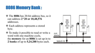
 The 8086 has 20-bit address bus, so it
can address 2^20 or 10,48,576
addresses.
 Each address represents a stored
byte.
 To make it possible to read or write a
word with one machine cycle,
the memory for an 8086 is set up in to
2 banks of up to 5,24,288 bytes each.
Memory Organization in 8086 :
 Memory IC’s: Byte oriented
 Word: Stored by two consecutive
memory location for LSB and MSB
 Address of Word: Address of LSB
 Bank 0: 𝑨°= 0 Even Address
Memory Bank
 Bank 1: 𝑩𝑯𝑬=0 Odd Address
Memory Bank
8086 Memory Addressing :
Data can be accessed from the memory in four different ways:
 8 - bit data from Lower (Even) address Bank.
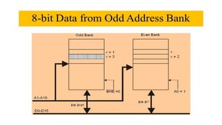
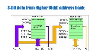
 8 - bit data from Higher (Odd) address Bank.
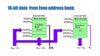
 16 - bit data starting from Even Address.
 16 - bit data starting from Odd Address.
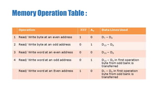
Memory Operation Table :
Accessing 8-bit data from Lower (Even)
address bank :
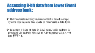
 The two bank memory module of 8086 based storage
system requires one bus- cycle to read/write a data-byte.
 To access a Byte of data in Low-bank, valid address is
provided via address pins A1 to A19 together with 𝐴°= 0
and 𝐵𝐻𝐸= 1.
8-bit data from Lower (Even) address bank:
Accessing 8-bit data from Higher (Odd)
address bank :
 To access a Byte of data in High-bank,valid address in pins A1 to
A19, 𝐴°= 1 and 𝐵𝐻𝐸= 0 are required to access the data through D8 to
D15 of the data-bus.
 These signals disable the Low bank and enable the High bank to
transfer (in/out) data through D8 to D15 of the data-bus.
8-bit data from Higher (Odd) address bank:
Accessing 16 - bit data starting from Even
Address :
 For even-addressed (aligned) words, only one bus-cycle is needed
to access the word, as both low and high banks are activated at the
same time using 𝐴°= 0 and 𝐵𝐻𝐸= 0.
 Note that during this bus-cycle, all 16-bit data is transferred via D0
to D15 of the data bus.
16-bit data from Even address bank:
Accessing 16 - bit data
starting from Odd Address :
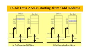
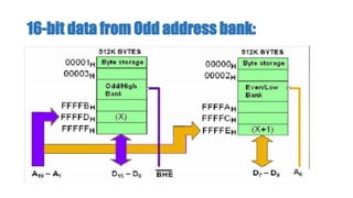
 For odd-addressed (unaligned) words (with odd P.A of the LSB), two
bus-cycles are required to access the Word-data.
 During the 1st bus-cycle, odd addressed LSB of the word is accessed
from the High-memory-bank via D8 to D15 of data bus.
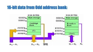
 During 2nd bus-cycle, P.A. is auto-incremented to access the even
address MSB of the word from the Low bank via D0 to D7.
 Note that 𝐴° and 𝐵𝐻𝐸 signals are reset (violet) accordingly to enable
the required memory bank.
16-bit data from Odd address bank:
Memory banking-of-8086-final

Memory banking-of-8086-final

  • 1.
    Memory Banking of8086 Group Members : Ibrahim Adham Mesu : 171-15-9543 Ali Asraf Munna :171-15-9511 Tofayel Ahmed :171-15-9521 Sakib Hasan Rial :171-15-9535 Nasim Bin Kamal :171-15-9511
  • 2.
    Content:  Memory Bank. Memory Organization.  Memory Addressing Bank.  Operation Table.  Accessing Address Bank.
  • 3.
    8086 Memory Bank:  The 8086 has 20-bit address bus, so it can address 2^20 or 10,48,576 addresses.  Each address represents a stored byte.  To make it possible to read or write a word with one machine cycle, the memory for an 8086 is set up in to 2 banks of up to 5,24,288 bytes each.
  • 4.
    Memory Organization in8086 :  Memory IC’s: Byte oriented  Word: Stored by two consecutive memory location for LSB and MSB  Address of Word: Address of LSB  Bank 0: 𝑨°= 0 Even Address Memory Bank  Bank 1: 𝑩𝑯𝑬=0 Odd Address Memory Bank
  • 5.
    8086 Memory Addressing: Data can be accessed from the memory in four different ways:  8 - bit data from Lower (Even) address Bank.  8 - bit data from Higher (Odd) address Bank.  16 - bit data starting from Even Address.  16 - bit data starting from Odd Address.
  • 6.
  • 7.
    Accessing 8-bit datafrom Lower (Even) address bank :  The two bank memory module of 8086 based storage system requires one bus- cycle to read/write a data-byte.  To access a Byte of data in Low-bank, valid address is provided via address pins A1 to A19 together with 𝐴°= 0 and 𝐵𝐻𝐸= 1.
  • 9.
    8-bit data fromLower (Even) address bank:
  • 10.
    Accessing 8-bit datafrom Higher (Odd) address bank :  To access a Byte of data in High-bank,valid address in pins A1 to A19, 𝐴°= 1 and 𝐵𝐻𝐸= 0 are required to access the data through D8 to D15 of the data-bus.  These signals disable the Low bank and enable the High bank to transfer (in/out) data through D8 to D15 of the data-bus.
  • 12.
    8-bit data fromHigher (Odd) address bank:
  • 13.
    Accessing 16 -bit data starting from Even Address :  For even-addressed (aligned) words, only one bus-cycle is needed to access the word, as both low and high banks are activated at the same time using 𝐴°= 0 and 𝐵𝐻𝐸= 0.  Note that during this bus-cycle, all 16-bit data is transferred via D0 to D15 of the data bus.
  • 15.
    16-bit data fromEven address bank:
  • 16.
    Accessing 16 -bit data starting from Odd Address :  For odd-addressed (unaligned) words (with odd P.A of the LSB), two bus-cycles are required to access the Word-data.  During the 1st bus-cycle, odd addressed LSB of the word is accessed from the High-memory-bank via D8 to D15 of data bus.  During 2nd bus-cycle, P.A. is auto-incremented to access the even address MSB of the word from the Low bank via D0 to D7.  Note that 𝐴° and 𝐵𝐻𝐸 signals are reset (violet) accordingly to enable the required memory bank.
  • 18.
    16-bit data fromOdd address bank:
  • 19.
    16-bit data fromOdd address bank: