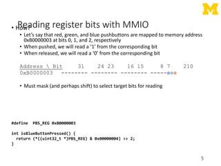
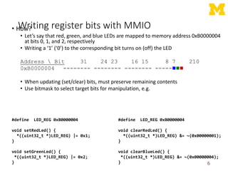
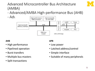
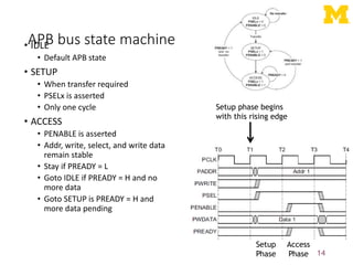
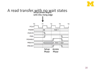
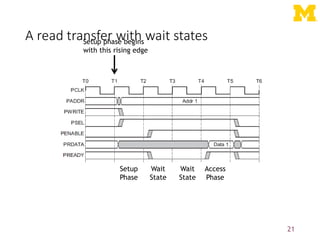
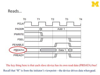
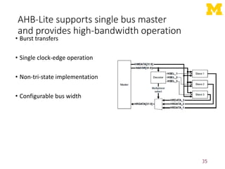
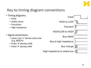
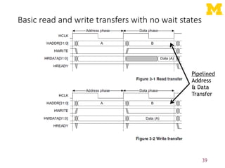
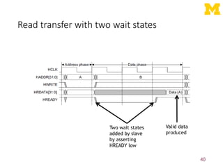
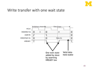
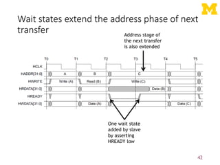
The document discusses Advanced Microcontroller Bus Architecture (AMBA) specifications including the Advanced Peripheral Bus (APB) and AMBA High-performance Bus (AHB). It provides an overview of the APB, which is suitable for many low-speed peripherals. Key APB signals and the APB state machine are described. Examples of APB read and write transfers are shown, including those with wait states. The document also discusses the AHB, which supports higher performance features like pipelined operations, burst transfers, and multiple bus masters. Key AHB signals and examples of different transfer types are illustrated with timing diagrams.


![Design a device which writes to a register
whenever
any address in its range is written
25
32-bit Reg
D[31:0]
Q[31:0]
EN
C
We are assuming APB only gets lowest 8 bits of address here…
What if we want to have the LSB of this register control an
LED?
PREADY
PWDATA[31:0]
PWRITE
PENABLE
PSEL
PADDR[7:0]
PCLK
LED](https://image.slidesharecdn.com/amba-220927044830-505fda6c/85/amba-ppt-25-320.jpg)
![Reg A should be written at address 0x00001000
Reg B should be written at address 0x00001004
26
32-bit Reg A
D[31:0]
Q[31:0]
EN
C
We are assuming APB only gets lowest 8 bits of address here…
32-bit Reg B
D[31:0]
Q[31:0]
EN
C
PREADY
PWDATA[31:0]
PWRITE
PENABLE
PSEL
PADDR[7:0]
PCLK](https://image.slidesharecdn.com/amba-220927044830-505fda6c/85/amba-ppt-26-320.jpg)
![Let’s say we want a device that provides data from
a switch on a read to any address it is assigned.
(so returns a 0 or 1)
28
Mr.
Switch
PWRITE
PENABLE
PSEL
PADDR[7:0]
PCLK
PREADY
PRDATA[32:0]](https://image.slidesharecdn.com/amba-220927044830-505fda6c/85/amba-ppt-28-320.jpg)
![Device provides data from switch A if address
0x00001000 is read from. B if address 0x00001004
is read from
29
Mr.
Switch
Mrs.
Switch
PWRITE
PENABLE
PSEL
PADDR[7:0]
PCLK
PREADY
PRDATA[31:0]](https://image.slidesharecdn.com/amba-220927044830-505fda6c/85/amba-ppt-29-320.jpg)
![All reads read from register, all writes write…
30
PWDATA[31:0]
PWRITE
PENABLE
PSEL
PADDR[7:0]
PCLK
PREADY
32-bit Reg
D[31:0]
Q[31:0]
EN
C
We are assuming APB only gets lowest 8 bits of address here…
PREADY
PRDATA[31:0]](https://image.slidesharecdn.com/amba-220927044830-505fda6c/85/amba-ppt-30-320.jpg)
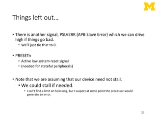
![Verilog!
32
/*** APB3 BUS INTERFACE ***/
input PCLK, // clock
input PRESERN, // system reset
input PSEL, // peripheral select
input PENABLE, // distinguishes access phase
output wire PREADY, // peripheral ready signal
output wire PSLVERR, // error signal
input PWRITE, // distinguishes read and write cycles
input [31:0] PADDR, // I/O address
input wire [31:0] PWDATA, // data from processor to I/O device (32 bits)
output reg [31:0] PRDATA, // data to processor from I/O device (32-bits)
/*** I/O PORTS DECLARATION ***/
output reg LEDOUT, // port to LED
input SW // port to switch
);
assign PSLVERR = 0;
assign PREADY = 1;](https://image.slidesharecdn.com/amba-220927044830-505fda6c/85/amba-ppt-32-320.jpg)
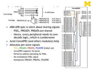
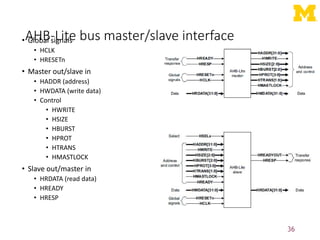
![AHB-Lite signal definitions
• Global signals
• HCLK: the bus clock source (rising-edge triggered)
• HRESETn: the bus (and system) reset signal (active low)
• Master out/slave in
• HADDR[31:0]: the 32-bit system address bus
• HWDATA[31:0]: the system write data bus
• Control
• HWRITE: indicates transfer direction (Write=1, Read=0)
• HSIZE[2:0]: indicates size of transfer (byte, halfword, or word)
• HBURST[2:0]: indicates single or burst transfer (1, 4, 8, 16 beats)
• HPROT[3:0]: provides protection information (e.g. I or D; user or handler)
• HTRANS: indicates current transfer type (e.g. idle, busy, nonseq, seq)
• HMASTLOCK: indicates a locked (atomic) transfer sequence
• Slave out/master in
• HRDATA[31:0]: the slave read data bus
• HREADY: indicates previous transfer is complete
• HRESP: the transfer response (OKAY=0, ERROR=1)
37](https://image.slidesharecdn.com/amba-220927044830-505fda6c/85/amba-ppt-37-320.jpg)
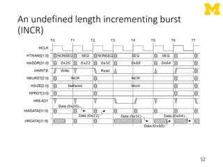
![Transfers can be of four types (HTRANS[1:0])
• IDLE (b00)
• No data transfer is required
• Slave must OKAY w/o waiting
• Slave must ignore IDLE
• BUSY (b01)
• Insert idle cycles in a burst
• Burst will continue afterward
• Address/control reflects next transfer in burst
• Slave must OKAY w/o waiting
• Slave must ignore BUSY
• NONSEQ (b10)
• Indicates single transfer or first transfer of a burst
• Address/control unrelated to prior transfers
• SEQ (b11)
• Remaining transfers in a burst
• Addr = prior addr + transfer size
44](https://image.slidesharecdn.com/amba-220927044830-505fda6c/85/amba-ppt-44-320.jpg)
![A four beat burst with master busy and slave
wait
45
One wait state
added by slave
by asserting
HREADY low
Master busy
indicated by
HTRANS[1:0]](https://image.slidesharecdn.com/amba-220927044830-505fda6c/85/amba-ppt-45-320.jpg)
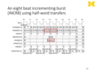
![Controlling the size (width) of a transfer
• HSIZE[2:0] encodes the size
• The cannot exceed the data bus width
(e.g. 32-bits)
• HSIZE + HBURST is determines
wrapping boundary for wrapping
bursts
• HSIZE must remain constant
throughout a burst transfer
46](https://image.slidesharecdn.com/amba-220927044830-505fda6c/85/amba-ppt-46-320.jpg)
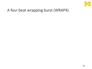
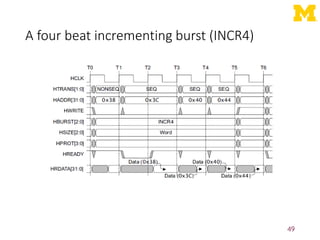
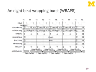
![Controlling the burst beats (length) of a
transfer
• Burst of 1, 4, 8, 16, and undef
• HBURST[2:0] encodes the type
• Incremental burst
• Wrapping bursts
• 4 beats x 4-byte words wrapping
• Wraps at 16 byte boundary
• E.g. 0x34, 0x38, 0x3c, 0x30,…
• Bursts must not cross 1KB address
boundaries
47](https://image.slidesharecdn.com/amba-220927044830-505fda6c/85/amba-ppt-47-320.jpg)