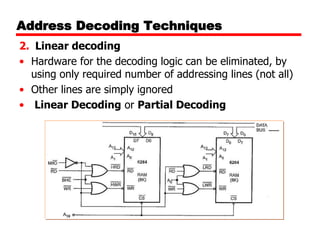
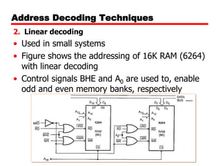
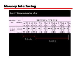
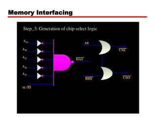
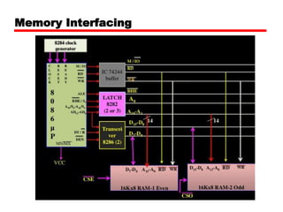
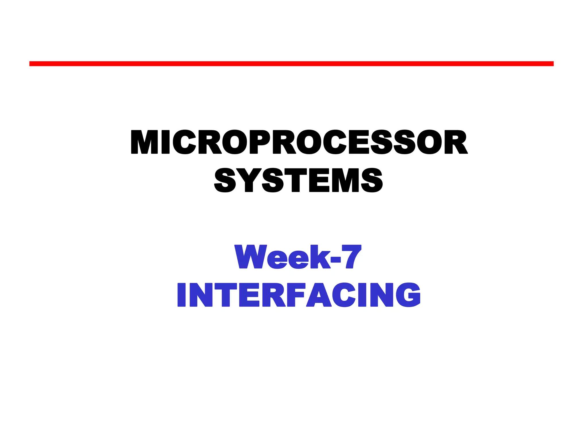
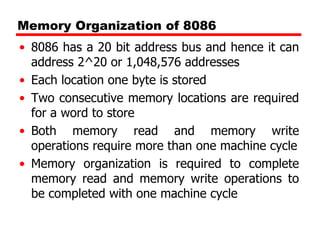
The document discusses memory organization and interfacing for the 8086 microprocessor. It describes how the 8086's 20-bit address bus is used to address 1MB of memory in two banks - an even bank using address lines A0 and D0-D7, and an odd bank using the complement of A0 and D8-D15. It provides examples of byte and word transfers to even and odd addresses, and compares the cycles, lines, and control signals used. Address decoding techniques like absolute, linear, and block decoding are also summarized. An example is given to interface 32KB of RAM using absolute decoding.
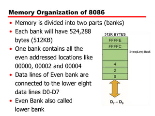
![Memory Organization (Data Transfer)
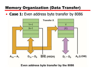
• Case 1: Even address byte transfer by 8086
• Read/Write a byte form/to an even address
• A0 will be low
• BHE (Active Low) will be high
• Byte is transferred to/from low bank through
D0-D7
• One Machine Cycle required
• Example
MOV AH,DS:BYTE PTR[0000]](https://image.slidesharecdn.com/addressdecoding1-230810193536-d70f3553/85/Address-decoding-1-pptx-6-320.jpg)
![Memory Organization (Data Transfer)
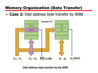
• Case 2: Odd address byte transfer by 8086
• Read/Write a byte from/to an odd address
• A0 will be high
• BHE (Active Low) will be asserted low
• Low bank is disabled and high bank is enabled
• Byte is transferred through D0-D7
• One Machine Cycle required
• Example
MOV AL,DS:BYTE PTR[0001]](https://image.slidesharecdn.com/addressdecoding1-230810193536-d70f3553/85/Address-decoding-1-pptx-8-320.jpg)
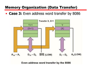
![Memory Organization (Data Transfer)
• Case 3: Even address word transfer by 8086
• A0 will be asserted low – Low byte of the word
through D0-D7
• BHE (Active Low) will be asserted low –high
byte of the word through D8-D15
• One Machine Cycle required
• Example
MOV AX,DS:WORD PTR[0000]](https://image.slidesharecdn.com/addressdecoding1-230810193536-d70f3553/85/Address-decoding-1-pptx-10-320.jpg)
![Memory Organization (Data Transfer)
• Case 4: Odd address word transfer by 8086
• Read/Write a word from/to an odd address
• Two bus cycles are required
• During the first machine cycle assert BHE
(Active Low) as low and A0 as high
• First byte is transferred through D0-D7 and the
second byte is transferred through D8-D15
• Example
MOV AX,DS:WORD PTR[0001H]](https://image.slidesharecdn.com/addressdecoding1-230810193536-d70f3553/85/Address-decoding-1-pptx-12-320.jpg)