This document summarizes a lecture on power amplifiers, including:
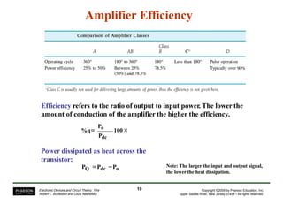
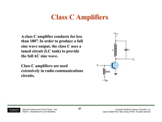
- Different classes of power amplifiers like Class A, B, AB, C, and D based on conduction angle.
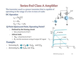
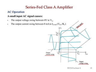
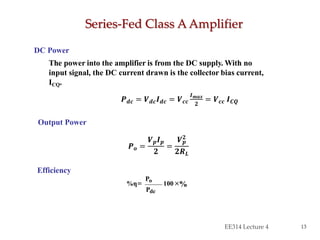
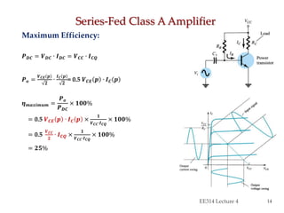
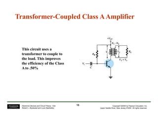
- Circuit designs for series-fed and transformer-coupled Class A amplifiers.
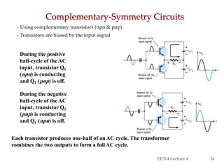
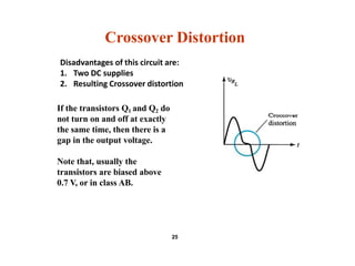
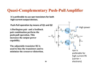
- Circuit designs for Class B amplifier using complementary pairs or a Darlington pair to achieve push-pull operation.
- Considerations for efficiency and maximum output power of different classes.


![RF Module Design - [Chapter 6] Power Amplifier](https://cdn.slidesharecdn.com/ss_thumbnails/rfch6-150613070347-lva1-app6891-thumbnail.jpg?width=640&height=640&fit=bounds)