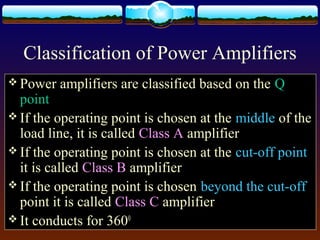
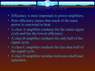
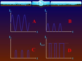
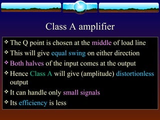
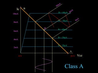
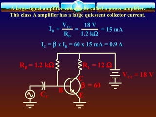
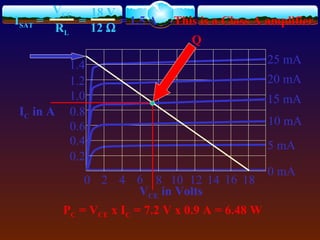
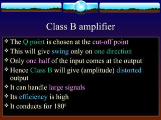
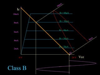
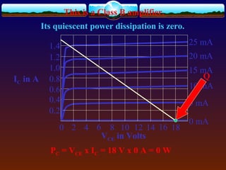
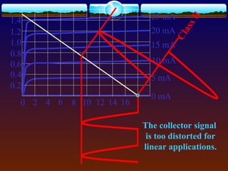
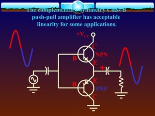
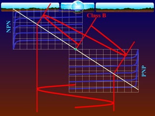
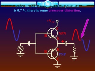
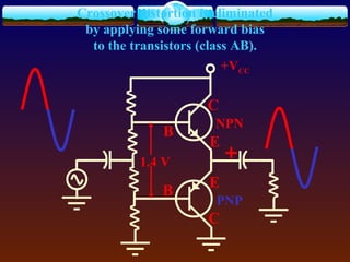
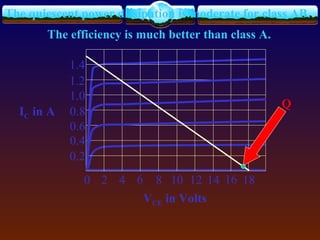
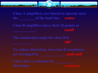
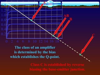
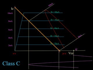
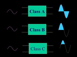
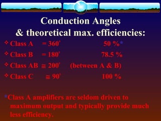
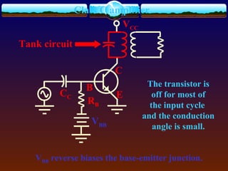
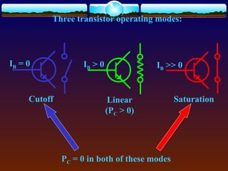
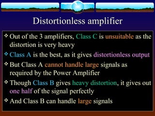
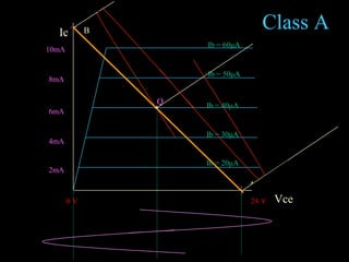
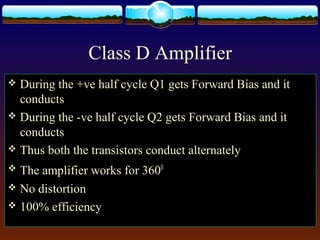
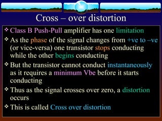
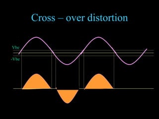
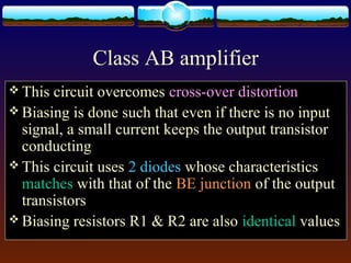
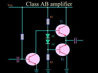
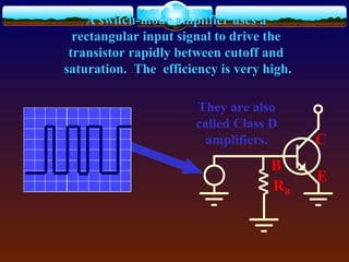
Power amplifiers are classified based on their operating point or quiescent point (Q point). Class A amplifiers have their Q point at the center of the load line, resulting in linear but low efficiency operation. Class B amplifiers operate with their Q point at cutoff, providing high efficiency but distorted output. Class AB reduces distortion by adding some forward bias. Class D amplifiers switch between cutoff and saturation at a high frequency for very high efficiency operation suitable for audio.


![July07 4[1].1 power_amplifiers01](https://cdn.slidesharecdn.com/ss_thumbnails/july0741-200727121307-thumbnail.jpg?width=640&height=640&fit=bounds)


