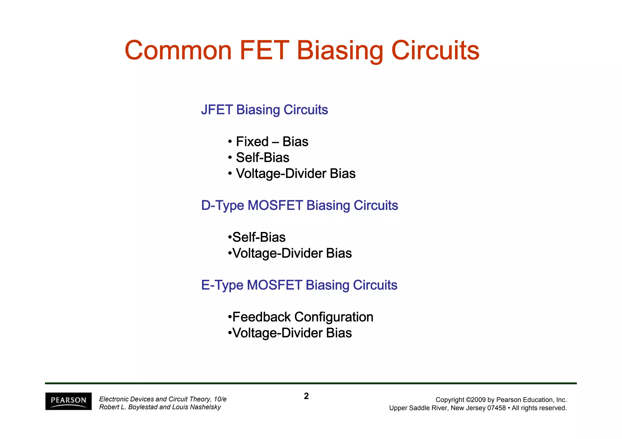
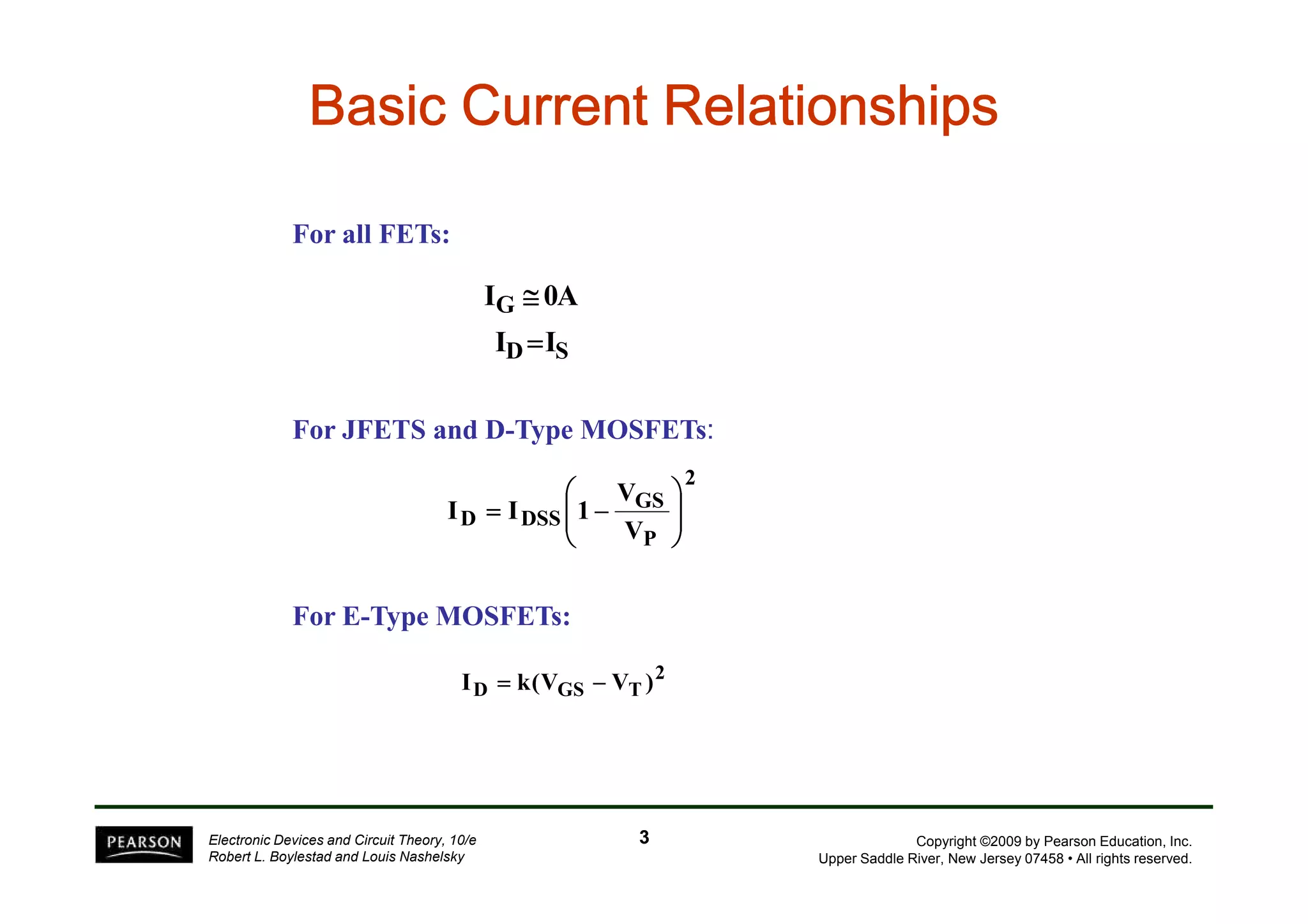
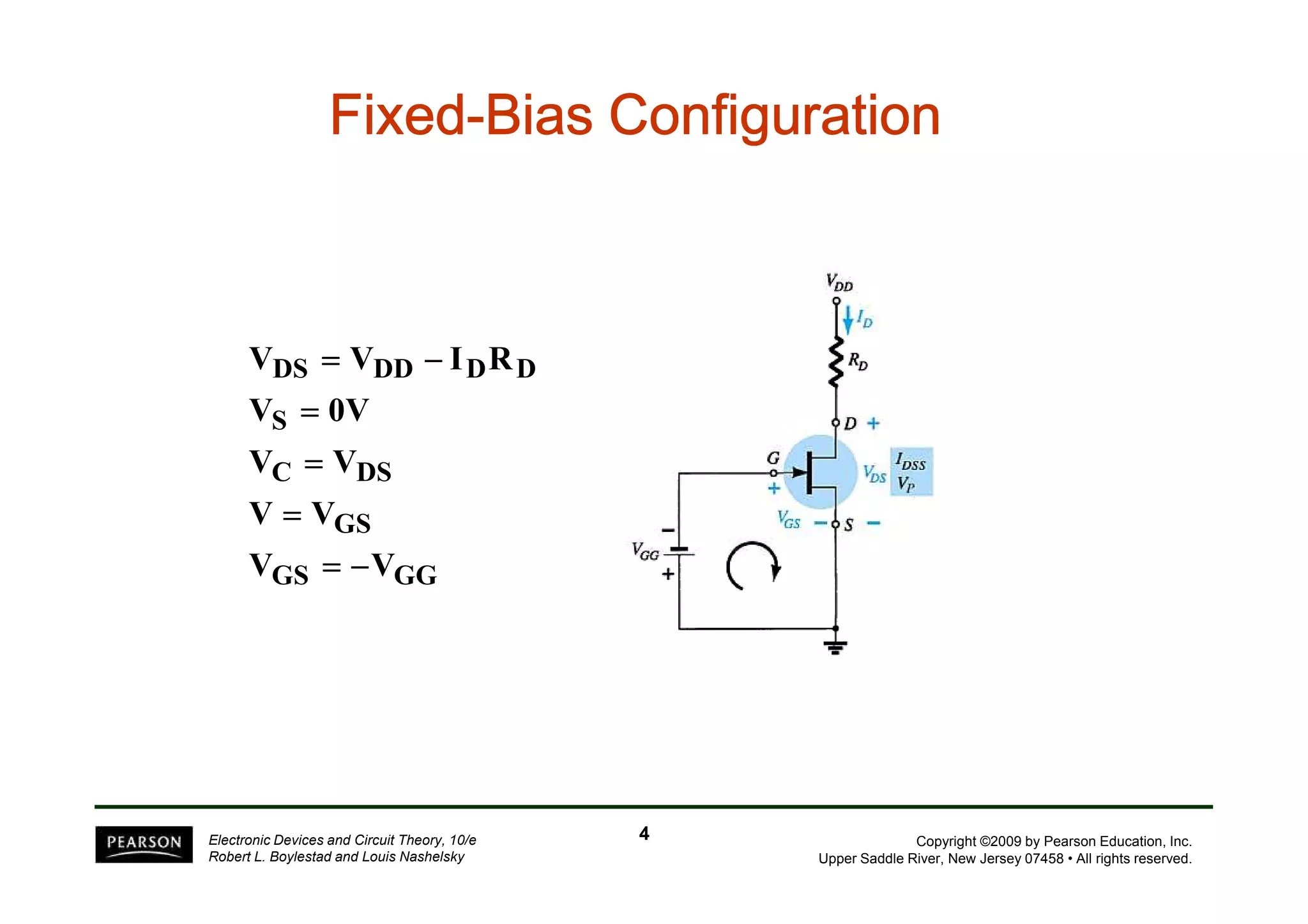
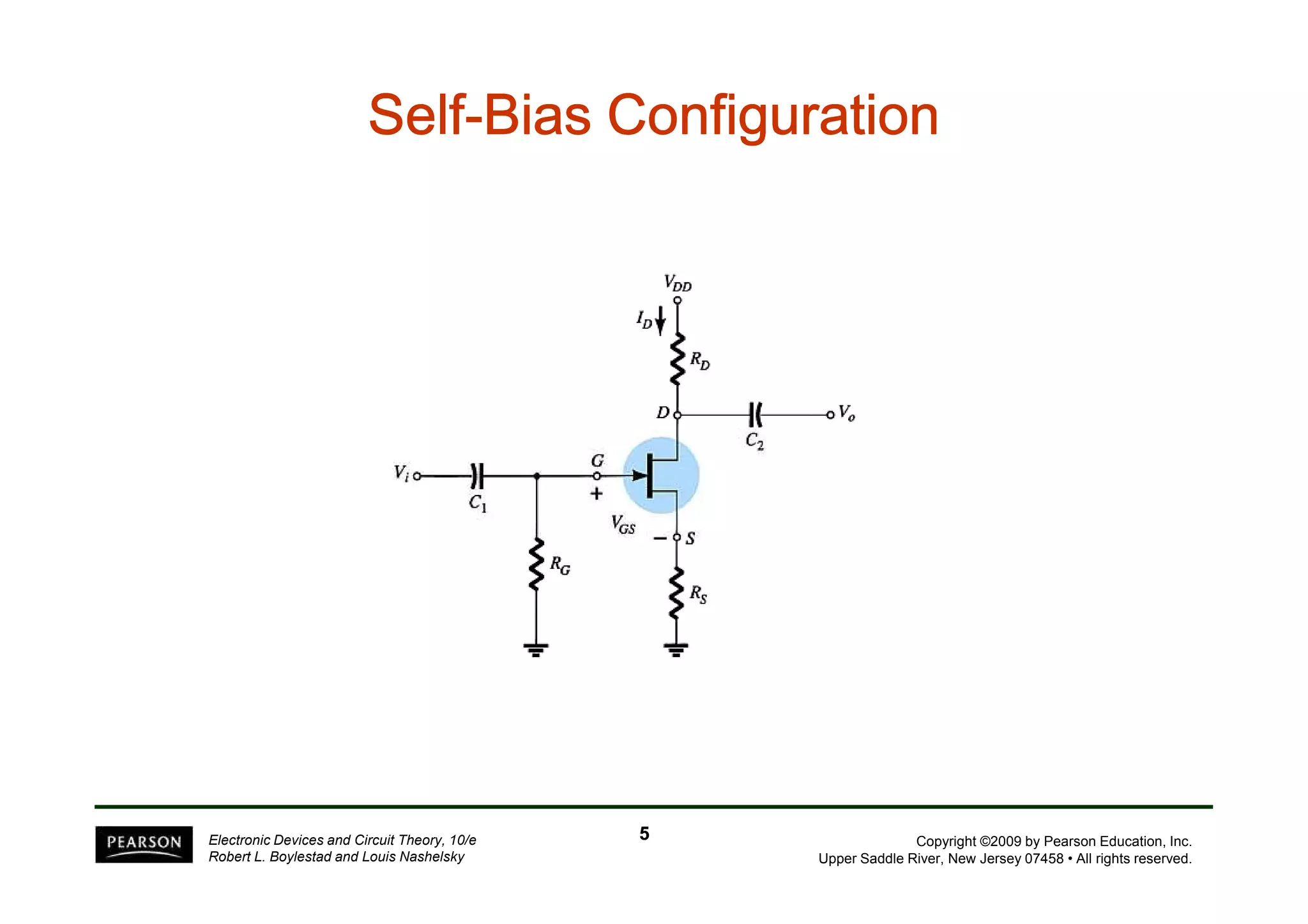
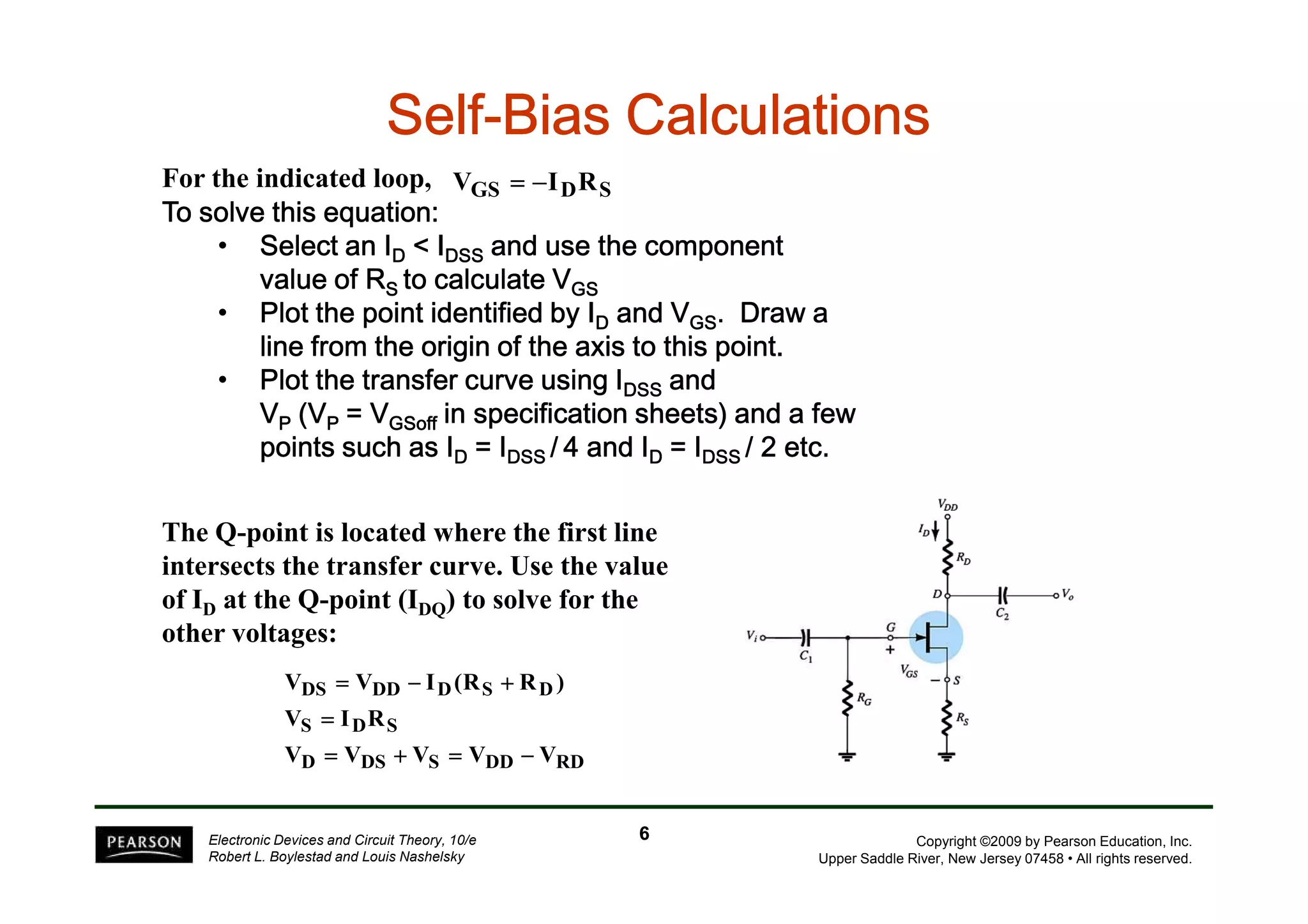
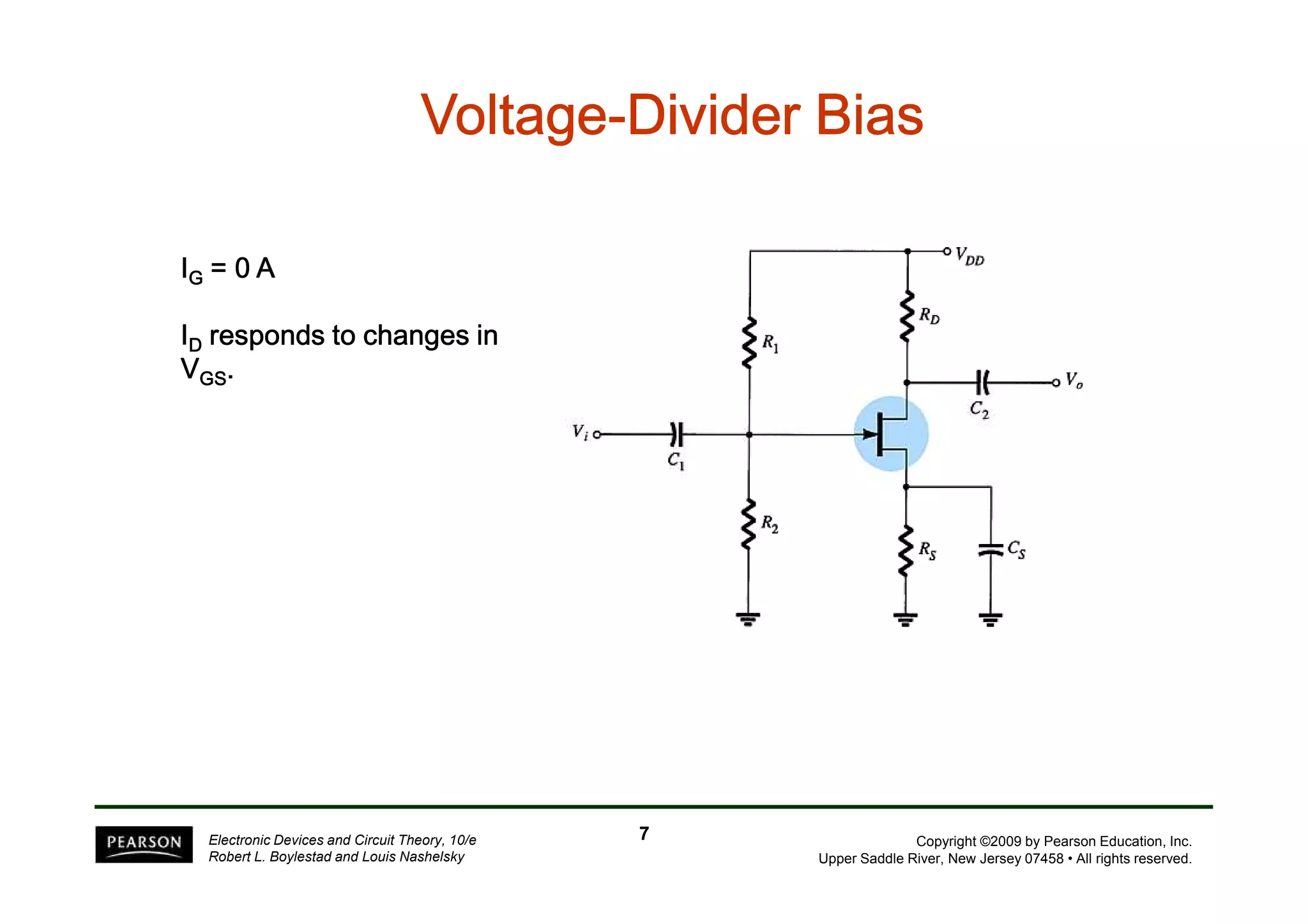
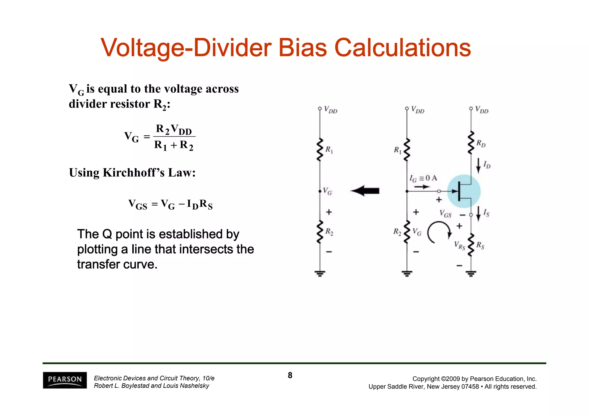
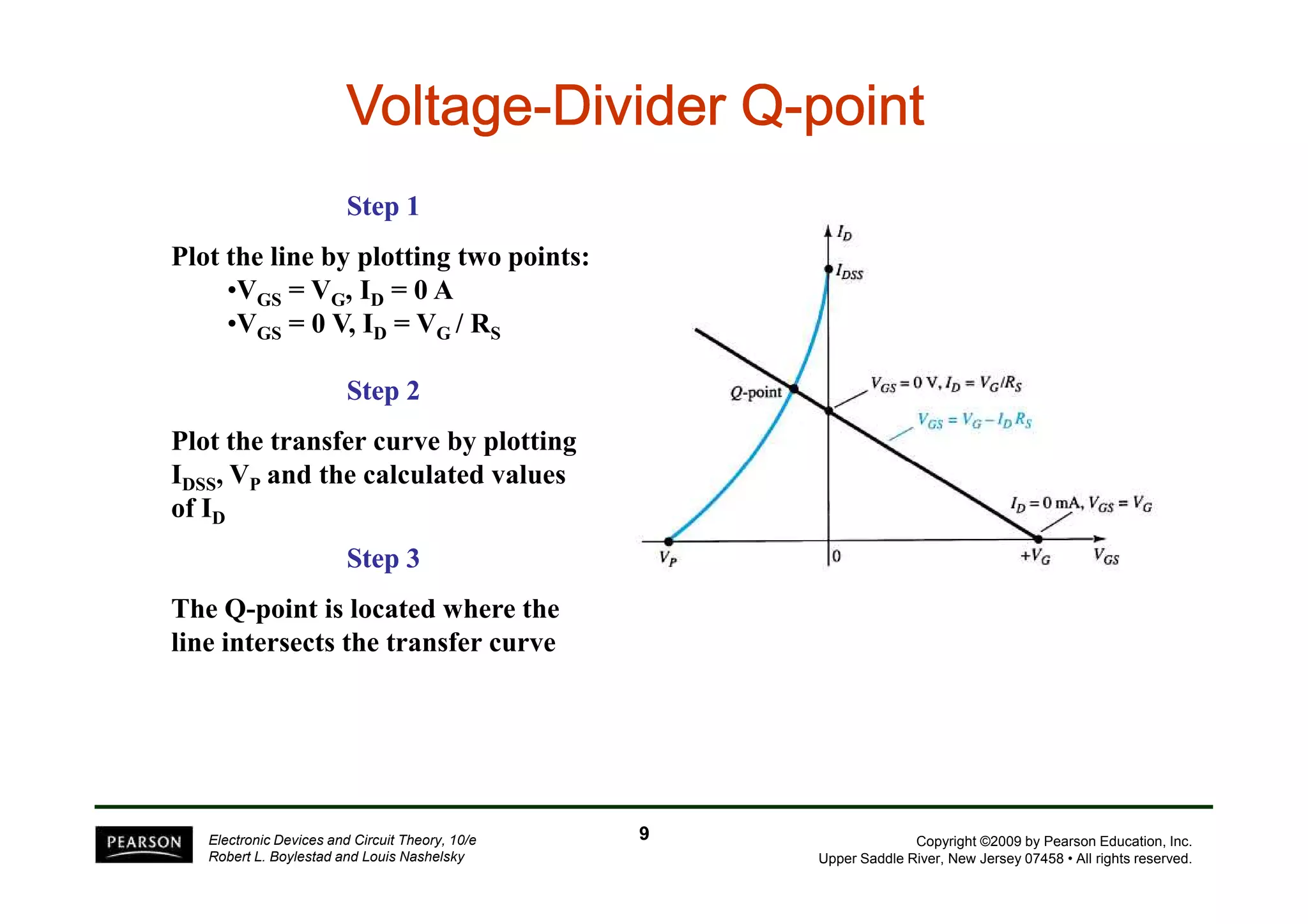
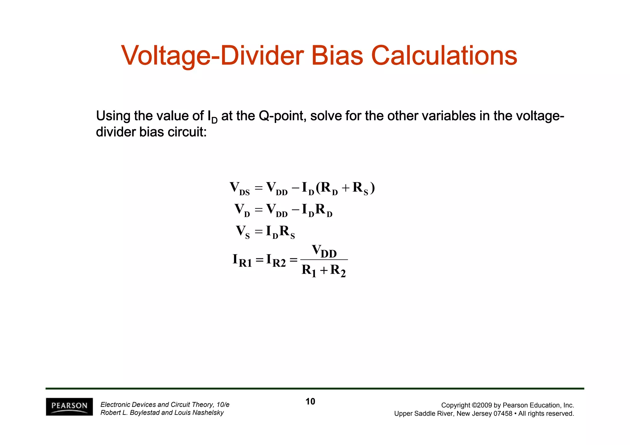
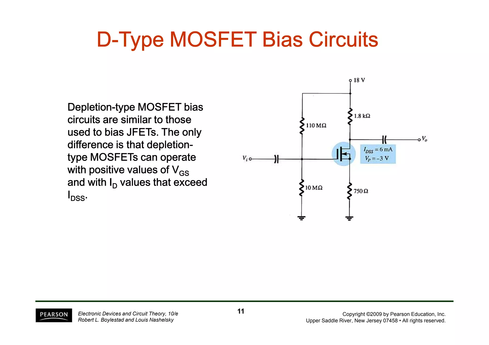
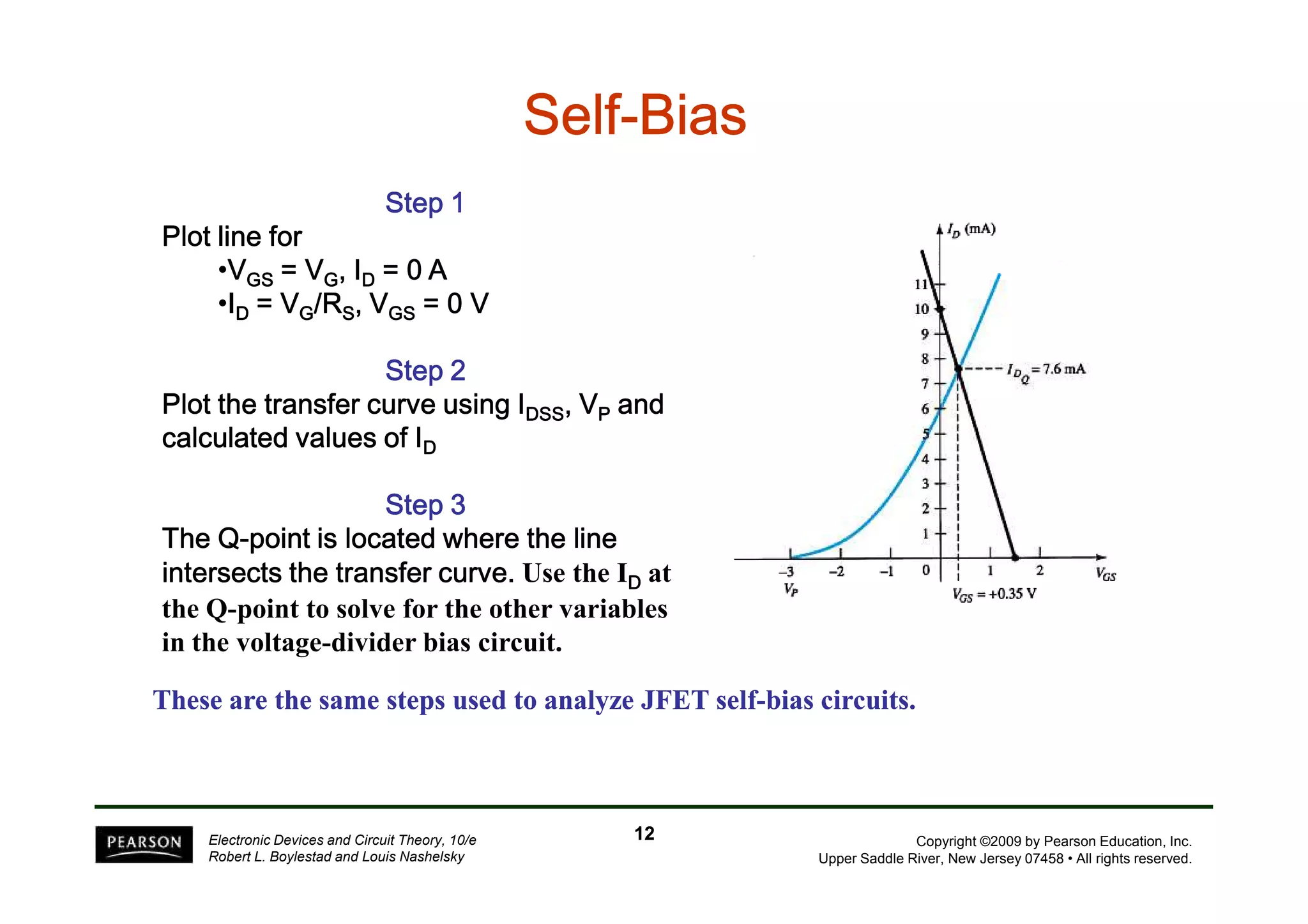
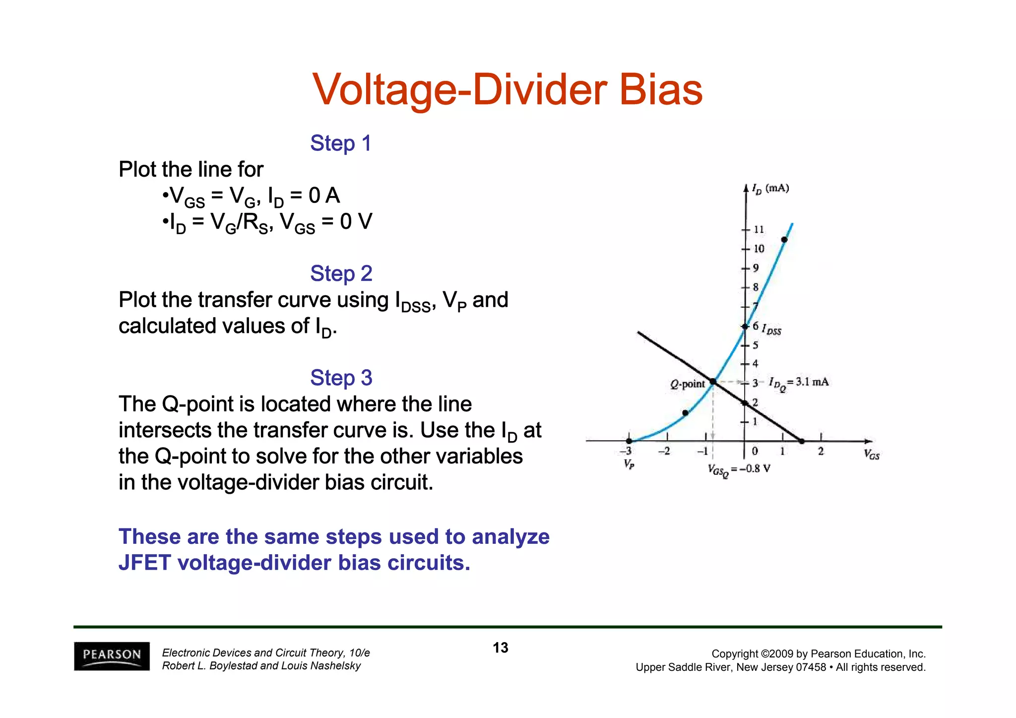
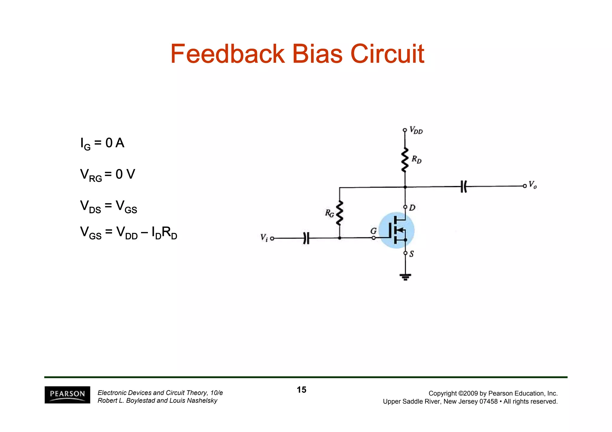
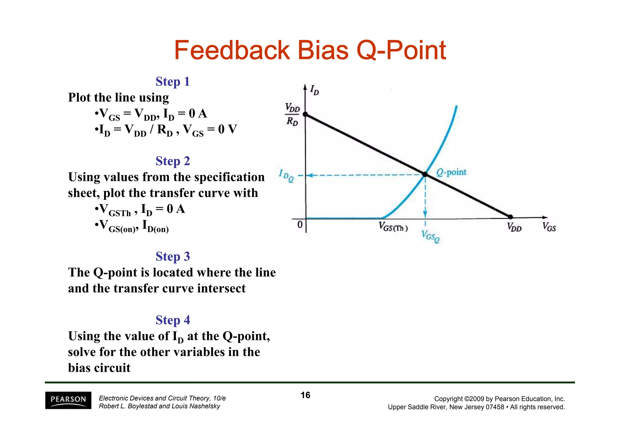
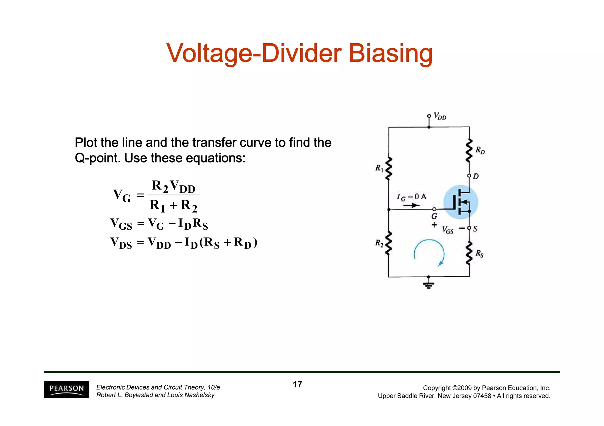
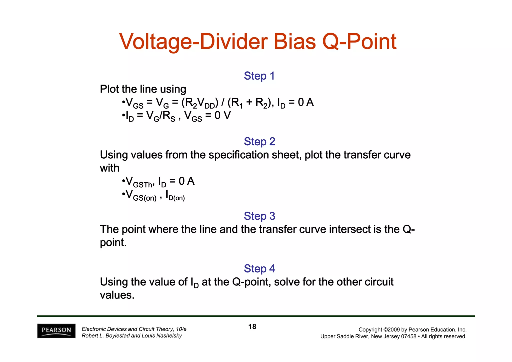
This chapter discusses various biasing circuits used for field effect transistors (FETs). It describes fixed-bias, self-bias, and voltage divider bias configurations for JFETs and MOSFETs. The key steps to analyze self and voltage divider bias circuits are: 1) Plot the transistor transfer curve and bias line, 2) Find the Q-point where they intersect, 3) Use the Q-point values to calculate the other circuit voltages and currents. D-type MOSFET biasing is similar to JFET biasing, except they can operate with positive VGS values and higher ID values than IDSS.
This chapter discusses FET amplifiers. It describes the common FET configurations including common-source, common-gate, and common-drain. It provides the small-signal models and defines terms like transconductance. It then gives the input and output impedances and voltage gain calculations for each configuration. Examples of biased circuits are also presented along with a troubleshooting guide.
There are two types of transistors, PNP and NPN. A transistor has three terminals - emitter, base, and collector. In an NPN transistor, the emitter-base junction is forward biased and the base-collector junction is reverse biased. There are three common transistor configurations - common-base, common-emitter, and common-collector. The common-emitter configuration is most widely used. A transistor can be used to amplify signals and its gain is determined by its beta value. Transistors have defined operating regions and limits that depend on the configuration.
Operational amplifiers (op-amps) are high gain differential amplifiers with very high input impedance and low output impedance. Op-amps can be connected in either open-loop or closed-loop configurations, with closed-loop providing feedback to control and reduce the gain. Common op-amp circuits include inverting and non-inverting amplifiers, unity followers, summing amplifiers, integrators, and differentiators. Op-amps have specifications including input offset voltage and input offset current, which can cause an output offset even when the input is zero.
The document discusses the frequency response of BJT and FET amplifiers. It explains that at low frequencies, coupling and bypass capacitors lower the gain, while at high frequencies, stray capacitances associated with the active device lower the gain. The frequency range where an amplifier operates with negligible effects from capacitors is called the mid-range or bandwidth. Bode plots are used to illustrate the cutoff frequencies and roll-off of gain outside this bandwidth. The various factors that determine the low and high frequency cutoffs are analyzed.
This document discusses different methods of biasing BJT transistors, including fixed bias, emitter-stabilized bias, and voltage divider bias circuits. It explains how the DC bias voltages establish an operating point (Q-point) for the transistor in either the active, cutoff, or saturation regions. Load line analysis is used to determine the transistor's Q-point based on the bias circuit components and supply voltage. Feedback circuits are also introduced to improve stability against variations in the transistor's beta value.
This document summarizes BJT transistor modeling and analysis techniques. It discusses two common models for small signal AC analysis: the re model and hybrid equivalent model. It then focuses on analyzing the re model in various BJT configurations including common-emitter, common-base, and emitter follower. Calculation of gains, impedances, and voltages are demonstrated for each configuration. Feedback pair and current mirror circuits are also briefly introduced.
This document discusses various op-amp applications including constant-gain amplifiers, voltage summing, voltage buffers, controlled sources, instrumentation circuits, and active filters. It provides circuit diagrams and equations for calculating gain, cutoff frequencies, and other parameters. Applications include non-inverting and inverting amplifiers, voltage followers, voltage-controlled voltage sources, and first-order high-pass, low-pass, and bandpass filters.
This document summarizes various linear-digital integrated circuits (ICs). It discusses comparators, digital-analog and analog-digital converters, timers, voltage-controlled oscillators, and phase-locked loop circuits. Comparators compare input voltages and output a high or low voltage. Digital converters translate between digital and analog formats while timers produce timed output pulses. Voltage-controlled oscillators vary output frequency with input voltage and phase-locked loops synchronize an oscillator's frequency to an input reference signal.
This document discusses various diode applications including load line analysis, rectifier circuits, clipping circuits, and voltage multiplier circuits. Rectifier circuits such as half-wave, full-wave, and voltage doublers are used to convert AC to DC power. Clipping and clamping circuits use diodes to limit output voltages. Voltage multiplier circuits step up voltage using combinations of diodes and capacitors. Practical applications include battery charging, overvoltage protection, and setting reference voltages.
This document discusses power supplies and voltage regulators. It covers the components of typical power supplies, including rectifiers to convert AC to DC, filter circuits to reduce ripple voltage, and voltage regulator circuits to maintain a constant output voltage. Two common voltage regulator configurations are described: discrete transistor regulators and integrated circuit regulators. The document provides examples of series and shunt voltage regulator circuits and discusses fixed, adjustable, and negative voltage regulator ICs.
The document discusses various applications of operational amplifiers (op-amps) including constant-gain amplifiers, voltage summing, voltage buffers, controlled sources, instrumentation circuits, and active filters. Op-amps can be used to create inverting and non-inverting amplifiers, sum voltages, buffer signals, and act as controlled sources for voltage or current. Instrumentation circuits include display drivers and instrumentation amplifiers. Active filters that can be created using op-amps include low-pass, high-pass, and bandpass filters by adding capacitors and resistors to filter voltages at certain cutoff frequencies.
This document discusses different classes of power amplifiers. Class A amplifiers conduct over the full 360 degrees of the input cycle but have low efficiency around 25%. Class B amplifiers conduct over 180 degrees and have higher efficiency of 78.5% but require two transistors for a full output cycle. Class AB is a compromise between the two. Class C conducts less than 180 degrees and uses a tuned circuit for output. Class D is for digital signals and requires pulse conversion circuits. Transformer coupling can improve class A efficiency to 50% by spreading out voltage and current swings.
The document summarizes key concepts about semiconductor diodes. It discusses how diodes are made from doped semiconductor materials like silicon and conduct current mainly in one direction. Diodes have different operating characteristics depending on whether they are forward biased, reverse biased, or at no bias. The document also covers diode testing methods and applications of diodes like in LEDs and zener diodes.
This chapter discusses various applications of diodes in circuits. It describes how the load line and characteristic curve determine the operating point of a diode in a circuit. It also summarizes the forward and reverse bias approximations for silicon and germanium diodes. The chapter then examines the behavior of diodes in DC series, parallel and combination circuits. It explores how diodes can be used for rectification, clipping, clamping and voltage regulation purposes. Specific circuits including half-wave, full-wave, bridge and voltage multiplier configurations are analyzed.
This chapter discusses various two-terminal devices including Schottky diodes, varactor diodes, power diodes, tunnel diodes, photodiodes, photoconductive cells, IR emitters, liquid crystal displays, solar cells, and thermistors. It provides brief descriptions of each device and their operating principles as well as common applications.
This document discusses feedback and oscillator circuits. It describes the effects of negative feedback on amplifiers, including lower gain but higher input impedance, more stable gain, improved frequency response, and lower output impedance. There are four types of feedback connections: voltage-series, voltage-shunt, current-series, and current-shunt. Oscillators require positive feedback where the overall gain equals one. Common oscillator circuits include phase-shift, Wien bridge, tuned, crystal, and unijunction oscillators.
This document presents an agenda for a lecture on diodes. It will introduce basic diode concepts like their composition and circuit models. It will discuss applications of diodes in circuits and different types of diodes like Zener diodes and light emitting diodes. The lecture will show real diode components and their usage. It will conclude with a summary of diodes and thank sources in a bibliography.
This chapter discusses bipolar junction transistors. It describes the basic transistor construction with PNP and NPN types. It explains transistor operation with forward biased base-emitter and reverse biased base-collector junctions. It also discusses currents in transistors including minority and majority carriers. Different transistor configurations - common base, common emitter, and common collector - are presented along with their input/output characteristics and operating regions. Key parameters like alpha, beta, and power dissipation are also covered.
The document discusses the basics of a P-N junction diode. It explains that a P-N junction diode is formed by doping one side of an intrinsic semiconductor with an acceptor material to make it P-type and the other side with a donor material to make it N-type. When unbiased, electron-hole pairs diffuse across the junction but are stopped by the depletion region. When forward biased, the depletion region decreases and carriers can flow across the junction. The current-voltage characteristics show that in forward bias the current increases exponentially with voltage, while in reverse bias the current is very small until breakdown occurs.
The document discusses the MOSFET (Metal-Oxide Semiconductor Field-Effect Transistor). It describes MOSFETs as having four terminals (source, gate, drain, body), but the body is often connected to the source, making it a three-terminal device. MOSFETs are widely used for switching and amplifying electronic signals and are the core component of integrated circuits due to their small size. The document then discusses the construction and working of a MOSFET, explaining how applying a voltage to the gate controls the channel between source and drain through which electrons or holes can flow.
A transistor can be used as a current source by biasing the emitter current through a resistor. Any change in the collector voltage will have little effect on the collector/load current as long as the transistor remains active and not saturated. In a common-emitter amplifier, a small signal at the base causes a corresponding change in the emitter current. This then causes an amplified change in the opposite direction at the collector through the collector resistor load, providing voltage gain.
Common Emitter Configuration and Collector CurveZeeshan Rafiq
This document discusses common emitter configuration in transistors. It describes:
- The common emitter configuration has the emitter common to both input and output terminals. It provides high gain and is widely used in amplifier designs.
- The input characteristics are similar to a diode with the output characteristics relating collector current (IC) to collector voltage (VCE) for different base currents (IB).
- The active, cutoff, and saturation regions are described on the output characteristics graph.
The operational amplifier, or op-amp, is a basic building block of analog electronic circuits that amplifies the difference between its input terminals. It has very high gain, typically around 100,000, and its output depends on the difference between the voltages at its two input terminals. By using negative feedback, most of the open-loop gain is canceled out, making the op-amp useful for various applications like non-inverting and inverting amplifiers, adders, integrators, and differentiators. An ideal op-amp has infinite gain, bandwidth, and input impedance and zero output impedance. Practical op-amps have limitations compared to the ideal but can still perform signal amplification and processing functions.
Transistor as a Switch aims to study and demonstrate how a transistor can function as a switch. The circuit uses a BC547 transistor connected to an LED and powered by a 5V supply. A 1Hz square wave input is applied to the base of the transistor. When the input is high, the transistor saturates and allows maximum current to flow through the LED, turning it on. When the input is low, the transistor cuts off and no current flows through the LED, turning it off. Observing the LED and collector output on an oscilloscope shows the transistor functioning as a switch, turning the LED and output signal on and off alternately and out of phase with the square wave input.
The unijunction transistor (UJT) is a three-terminal semiconductor device with a single PN junction. It exhibits a negative resistance characteristic, which makes it useful for oscillator circuits. The UJT consists of a lightly doped N-type silicon bar with a single P-type region forming the emitter junction. It has three terminals - base 1, base 2, and emitter. In its active mode, the UJT shows negative resistance, where increasing the emitter voltage initially causes the emitter current to decrease. This physical phenomenon is called conductivity modulation and is caused by injection of holes from the emitter into the base, decreasing the resistance between the emitter and base 1.
This document discusses diode theory and characteristics. It explains that a diode is a non-linear device because its current-voltage graph is not a straight line due to the barrier potential. It describes how a diode can be forward or reverse biased depending on how it is connected in a circuit. The knee voltage, ideal diode characteristics, and approximations that account for the barrier potential and bulk resistance are also covered. Load lines and how they are used to determine operating points are summarized.
This document discusses various semiconductor switching devices including SCRs, triacs, diacs, GTOs, LASCRs, and UJTs. It provides details on their construction, operation, applications, and key specifications. The SCR is described as a thyristor that conducts in one direction and remains latched on once triggered by a gate signal. Commutation circuits are needed to turn off an SCR. The triac can conduct in both directions like a diac and is triggered by a gate or breakover voltage.
This document discusses negative feedback in amplifiers. It defines feedback as part of the output signal being returned to the input. Negative feedback occurs when the feedback signal is out of phase with the input signal. There are four types of feedback classified by the sampling and mixing networks: voltage series, current series, current shunt, and voltage shunt. Negative feedback provides advantages like stabilized gain and operating point but results in reduced gain. It has applications in electronic amplifiers, regulated power supplies, and wideband amplifiers.
This document summarizes the structure and function of skin and fascia. It describes the layers of the epidermis and dermis, the cell types found in each, and their roles. It discusses the blood supply, lymphatics, and innervation of the skin. It also briefly outlines the structure and functions of the hypodermis/superficial fascia and deep fascia.
This document summarizes a presentation given by David López Sánchez on spinal osteopathic manipulative therapy. It provides an overview of osteopathic philosophy which views the body as a single unified system. It describes assessment techniques for somatic dysfunction including asymmetry and tissue changes. Mechanisms of spinal manipulation are discussed such as restoring range of motion and reducing nociception. The document concludes that osteopathy aims to optimize health and stimulate self-regulation rather than simply treat diseases.
Tensegrity structure is the minimal structure that can support a weight and oppose horizontal forces, that uses compression and tension, but experiences no torque
This document discusses electrical safety. It provides a brief history of electricity and defines key concepts like voltage and current. It outlines the dangers of electricity, like electrocution from 0.1 amperes held for over a second. Electrical mishaps can be caused by overloads or shorts. The document recommends safety procedures like wearing protective equipment, ensuring proper grounding, and using surge protectors to prevent accidents.
This document summarizes a lecture on power amplifiers, including:
- Different classes of power amplifiers like Class A, B, AB, C, and D based on conduction angle.
- Circuit designs for series-fed and transformer-coupled Class A amplifiers.
- Circuit designs for Class B amplifier using complementary pairs or a Darlington pair to achieve push-pull operation.
- Considerations for efficiency and maximum output power of different classes.
This document provides a technical and critical overview of risk management in Spain, with specific focus on operational control. It discusses general concepts of risk management and then details aspects of operational control from both a technical and critical perspective. An example is also provided on evaluating occupational risks through a case study approach using a risk management plan.
The document provides specifications for various parts of a vehicle including dimensions, identification, lifting, towing, lubricants, draining/refilling, tools, and complete engine and lower engine units. It lists specifications for items like oil consumption, oil pressure, packaging, and identifies engine/gearbox types including J8 and Z7X engines.
The document provides specifications for various parts of a vehicle's engine assembly and lower engine section. It lists engine models including their identifications. It details lubricants and consumables capacities, as well as procedures for checking engine oil pressure and identifying oil leaks. Exploded views of the engine assembly and components are also included.
This technical specification provides details for an LPG cylinder. It lists the height as 310mm, diameter as 270mm, average weight as 6kg and volume as 14.4L. Additional features noted are that it is a certified product that has passed all tests, and is an earth friendly product. Contact information is provided for more details.
This document contains specifications for an engine including dimensions, identification, lubricants, oil draining, tooling, and engine assembly information. It lists technical details for the engine across multiple sections and subsections with accompanying web links.
This document summarizes methods for advancing proton exchange membrane fuel cell technology. It discusses (1) reducing the platinum loading of electrodes by extending the reaction zone through three-dimensional structuring and incorporating a proton-conducting material, (2) optimizing the amount of incorporated material in the electrode structure, (3) pressing quantities of the electrodes onto the membrane at 120°C and 500 atm, (4) optimal humidification of reactant gases at a temperature above the cell, and (5) functioning at elevated pressures and temperatures. The document analyzes fuel cells based on methods of current density and voltammetry.
Similar to Electronic devices-and-circuit-theory-10th-ed-boylestad-chapter-7 (6)