Downloaded 83 times


![ExampleExample
Calculate the input power [Pi
(dc)], output power
[Po
(ac)], and efficiency [η] of the amplifier circuit for
an input voltage that results in a base current of
10mA peak.
RC
RB
+VCC = 20V
IC
Vi
25=β
Ω20
Ωk1
Vo
( )
%5.6%100
6.9)48.0)(20(
625.0)20(
2
10250
2
250)10(25
20
11000
20
20
4.10)20)(48.0(20
48.05.482)3.19(25
3.19
1
7.020
)(
)(
)(
232
)(
)(
)(
)()(
)(
=×=
===
=Ω
×
==
===
==
==
Ω
==
=Ω−=−=
≅===
=
Ω
−
=
−
=
−
dci
aco
CQCCdci
C
peakC
aco
C
CC
satc
B
P
P
WAVIVP
W
A
R
I
P
peakmApeakmAII
VVV
AmA
V
R
V
I
VAVRIVV
AmAmAII
mA
k
VV
R
VV
I
peakbpeakC
CCcutoffCE
CCCCCEQ
CQ
B
BECC
BQ
η
β
β](https://image.slidesharecdn.com/ecaunit5-190223151559/85/Eca-unit-5-33-320.jpg)
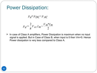
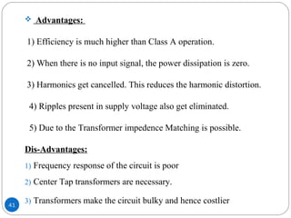
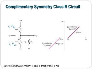
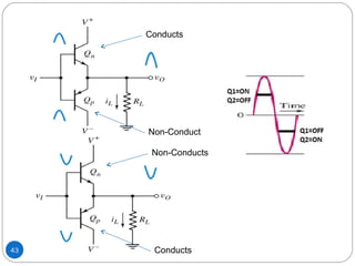
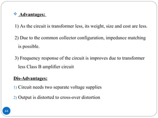
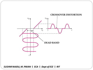
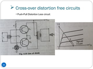
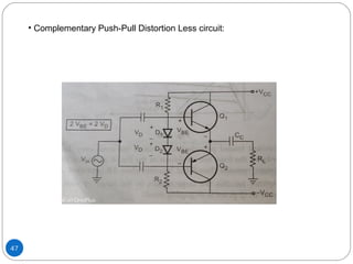
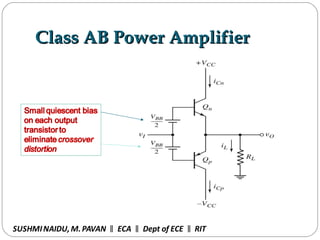
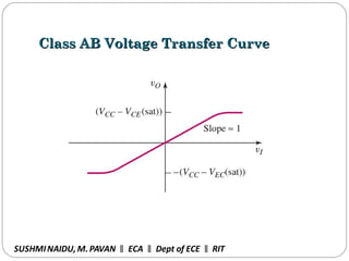
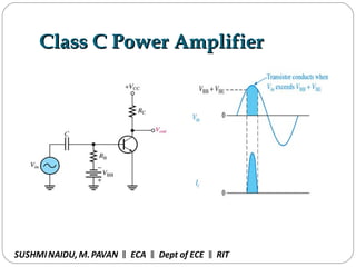
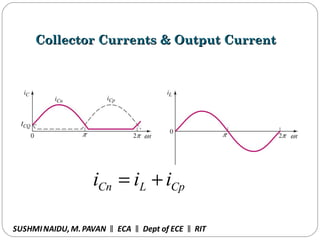
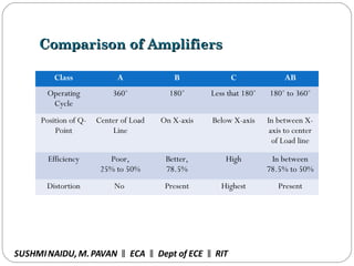
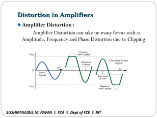
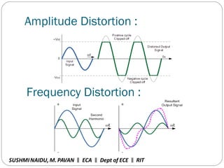


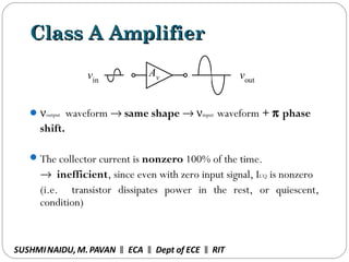
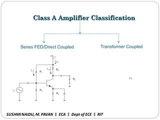
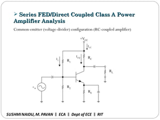
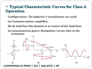
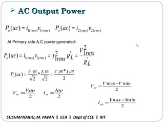
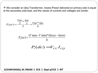
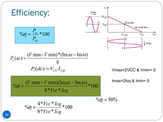
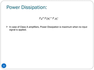
The document presents an analysis of various power amplifiers, including their classifications (Class A, B, AB, and C) and operational characteristics. It discusses the concepts of power dissipation, efficiency, and thermal stability, along with practical examples and considerations for their design and application. Additionally, it addresses advantages, disadvantages, and references for further study in electronic circuit analysis.


![RF Module Design - [Chapter 6] Power Amplifier](https://cdn.slidesharecdn.com/ss_thumbnails/rfch6-150613070347-lva1-app6891-thumbnail.jpg?width=640&height=640&fit=bounds)