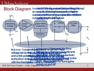
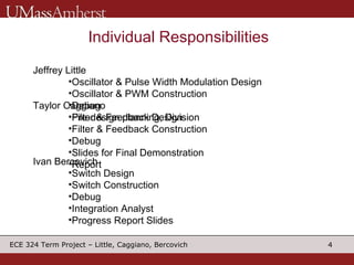
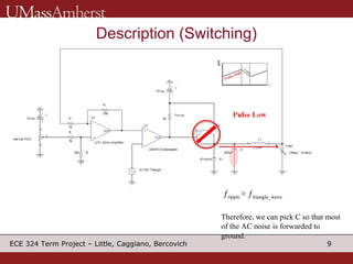
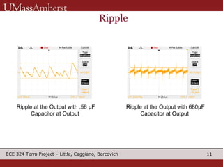
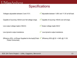
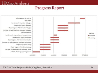
Switching Voltage Regulator Group 17 Jeffrey Little Taylor Caggiano Ivan Bercovich
Progress Report Block Diagram Description Individual Responsibilities Functionality Specifications Power Issues Summary
Block Diagram Reference Voltage : Adjustable voltage set by the 13V supply and a 50k potentiometer.  Input to the Error Amp and compared with the feedback. Error Amp : Linear amplifier made with a  741 Op Amp with a Gain of 50V/V.  Outputs an Error Voltage that determines the duty cycle of the pulse input to the switch.  Comparator : Compares the Error Voltage to a triangle wave (32 kHz oscillator).  Produces a pulse train with a duty cycle proportional to the error.  Responsible for turning the switch on and off. Switch : BJT Configuration (Sziklai Pair)- Turned on and off at the rhythm specified by the output pulse from the comparator.  Allows current to flow to the output. Filter : Maintains continuous voltage at output.  Inductor assures a constant current flow and capacitor filters 32kHz switching frequency.  Feedback : Feeds the output voltage to the Error Amp to be compared with the reference.
Individual Responsibilities Jeffrey Little Oscillator & Pulse Width Modulation Design  Oscillator & PWM Construction Debug Pre-design planning, Division Taylor Caggiano Filter & Feedback Design  Filter & Feedback Construction Debug Slides for Final Demonstration  Report  Ivan Bercovich  Switch Design  Switch Construction Debug Integration Analyst Progress Report Slides
Error Amplifier From Feedback From Reference To Comparator The gain of the linear amplifier is defined by a resistor ratio. In our case, we are using 50K (light) and 1K (dark) resistors in order to get a 50 V/V gain
From Analog Devices Application Note
Oscillator 741 Op Amp used as an integrator.  Comparator used to generate square wave by hitting the negative and positive rails. Frequency is defined by RC: Where Vs is the amplitude of the wave and Vp is the positive supply.
Switch “ Sziklai Pair” BJT Configuration Uses a NPN and PNP to supply more current  Current supplied is the product gain of the two transistors
ƒ ripple  ≈ ƒ triangle_wave. Therefore, we can pick C so that most of the AC noise is forwarded to ground. Description (Switching)
Duty Cycle = T HIGH /T≈ Vo Functionality
Ripple Ripple at the Output with .56 µF Capacitor at Output  Ripple at the Output with 680µF Capacitor at Output
DEMONSTRATE FUNCTIONALITY
Specifications Adjustable between 1.85V and 11.5V at full load. Capable of sourcing 145mA over all range. Output voltage ripple 30mV Low dynamic output resistance. Efficiency 50% @ 2V -> 84% @ 11.5V Voltages adjustable between 2 and 10 V. Capable of sourcing 120mA over full voltage range. Low output voltage ripple (<50mV) Low dynamic output resistance. Efficiency 50%,  η =(Power Supplied to the load)/(Total Power Consumed)
Progress Report
Summary Pulse Width Modulation Design Goal : Creating a pulse train with a duty cycle that depends on the input voltage.  Filter Circuitry Goal : Choose appropriate Capacitor value for the specified 1.1mH inductor.  Achieving required ripple spec. Note :  Calculated capacitor value is much smaller than actual. Switch Goal : Ensure total ON and OFF switching in response to pulses.  Transistor must be able to handle current and voltage required. Note : “Sziklai Pair” Method Implemented to increase current gain. Switch Driver & Feedback Loop Goal : Add protection diode and filter and see output voltage vary respectively with input to    PWM.  Connect feedback. Efficiency Measures Goal : Measure in appropriate locations for accurate calculations.  Measure ripple. Note :  Measure after supply filtering and at both ends of the voltage spec.
 

Switching Voltage Regulator

  • 1.
    Switching Voltage RegulatorGroup 17 Jeffrey Little Taylor Caggiano Ivan Bercovich
  • 2.
    Progress Report BlockDiagram Description Individual Responsibilities Functionality Specifications Power Issues Summary
  • 3.
    Block Diagram ReferenceVoltage : Adjustable voltage set by the 13V supply and a 50k potentiometer. Input to the Error Amp and compared with the feedback. Error Amp : Linear amplifier made with a 741 Op Amp with a Gain of 50V/V. Outputs an Error Voltage that determines the duty cycle of the pulse input to the switch. Comparator : Compares the Error Voltage to a triangle wave (32 kHz oscillator). Produces a pulse train with a duty cycle proportional to the error. Responsible for turning the switch on and off. Switch : BJT Configuration (Sziklai Pair)- Turned on and off at the rhythm specified by the output pulse from the comparator. Allows current to flow to the output. Filter : Maintains continuous voltage at output. Inductor assures a constant current flow and capacitor filters 32kHz switching frequency. Feedback : Feeds the output voltage to the Error Amp to be compared with the reference.
  • 4.
    Individual Responsibilities JeffreyLittle Oscillator & Pulse Width Modulation Design Oscillator & PWM Construction Debug Pre-design planning, Division Taylor Caggiano Filter & Feedback Design Filter & Feedback Construction Debug Slides for Final Demonstration Report Ivan Bercovich Switch Design Switch Construction Debug Integration Analyst Progress Report Slides
  • 5.
    Error Amplifier FromFeedback From Reference To Comparator The gain of the linear amplifier is defined by a resistor ratio. In our case, we are using 50K (light) and 1K (dark) resistors in order to get a 50 V/V gain
  • 6.
    From Analog DevicesApplication Note
  • 7.
    Oscillator 741 OpAmp used as an integrator. Comparator used to generate square wave by hitting the negative and positive rails. Frequency is defined by RC: Where Vs is the amplitude of the wave and Vp is the positive supply.
  • 8.
    Switch “ SziklaiPair” BJT Configuration Uses a NPN and PNP to supply more current Current supplied is the product gain of the two transistors
  • 9.
    ƒ ripple ≈ ƒ triangle_wave. Therefore, we can pick C so that most of the AC noise is forwarded to ground. Description (Switching)
  • 10.
    Duty Cycle =T HIGH /T≈ Vo Functionality
  • 11.
    Ripple Ripple atthe Output with .56 µF Capacitor at Output Ripple at the Output with 680µF Capacitor at Output
  • 12.
  • 13.
    Specifications Adjustable between1.85V and 11.5V at full load. Capable of sourcing 145mA over all range. Output voltage ripple 30mV Low dynamic output resistance. Efficiency 50% @ 2V -> 84% @ 11.5V Voltages adjustable between 2 and 10 V. Capable of sourcing 120mA over full voltage range. Low output voltage ripple (<50mV) Low dynamic output resistance. Efficiency 50%, η =(Power Supplied to the load)/(Total Power Consumed)
  • 14.
  • 15.
    Summary Pulse WidthModulation Design Goal : Creating a pulse train with a duty cycle that depends on the input voltage. Filter Circuitry Goal : Choose appropriate Capacitor value for the specified 1.1mH inductor. Achieving required ripple spec. Note : Calculated capacitor value is much smaller than actual. Switch Goal : Ensure total ON and OFF switching in response to pulses. Transistor must be able to handle current and voltage required. Note : “Sziklai Pair” Method Implemented to increase current gain. Switch Driver & Feedback Loop Goal : Add protection diode and filter and see output voltage vary respectively with input to PWM. Connect feedback. Efficiency Measures Goal : Measure in appropriate locations for accurate calculations. Measure ripple. Note : Measure after supply filtering and at both ends of the voltage spec.
  • 16.