SlideShare a Scribd company logo
1 of 17
Download to read offline
yayavaram@yahoo.com
1
Transient response of RC circuit with step input
Let us consider a circuit consisting of R and C in series with a Step input. A step signal is one
which has a voltage V0 at t < 0 and suddenly increase at t = 0 and remains constant Vs at t >>
0 as shown in the diagram.
By common sense we can understand that when t < 0, the capacitor will be charged to a constant
value V0 and the current in the circuit is zero.
At t = 0 , current will start flowing around circuit. This current will continue to flow as long
as there is a voltage difference across the Resistor.
Similarly at = infinity the input voltage rises to Vs and the voltage across the capacitor is Vs
which is a constant. So , the current through the circuit is zero.
Between the times t < 0 and t = infinity the current through the circuit increases gradually due
to the reactance of the Capacitor. This is also known as Transient response.
The total response of the circuit due to a step input signal can be considered as sum of two
responses. One is Natural response and the other is Forced response.
Total Response = Natural Response + Forced Response
Derivation:
At any instant of time t , let us assume that the voltage across the resistor is VR and voltage
across the Capacitor is Vc .
yayavaram@yahoo.com
2
Then VR= i.R and i = VR /R
The same current is passed through the Capacitor also. The current through the Capacitor is
i = C
𝑑𝑉
𝑑𝑡
where V is the voltage across the capacitor.
From the circuit VR = Vs – V
Therefore C
𝑑𝑉
𝑑𝑡
= VR /R =
Vs – V
𝑅
C
𝑑𝑉
𝑑𝑡
=
Vs
𝑅
-
V
𝑅
C
𝑑𝑉
𝑑𝑡
+
V
𝑅
=
Vs
𝑅
----------------------------(1)
This is a non-homogeneous Equation whose solution consists of two parts. One is
Complementary Function part ( i.e natural response at t = 0) and the other is Particular
Integral Part(i.e Forced response when t = œ).
Natural Response: Natural response of the circuit means, the response of the circuit without
any external signal. This circuit is shown below. The voltage across the Capacitor at any
instant is given by VN(t) = K.𝑒−𝑡/𝑅𝐶
--------------------------(2)
Here RC is called the Time Constant of the RC circuit. It has the units of time (sec)
Similarly the forced response means, the response of the circuitwhen external signal is
applied . In the present case the external input signal is Step Signal. At t = Infinity, the
voltage is equal to Vs .
Hence VF(t) = Vs -----------------------------(3)
So, the total response is VT = VN(t) + VF(t)
So, VT = K.𝑒−𝑡/𝑅𝐶
+ Vs
To find the value of the constant K ,let us apply the initial conditions .At t = 0
VT = V0 = K + Vs where V0 is the voltage when t =0
Or K = V0 – Vs
Hence VT = (V0 – Vs ) 𝒆−𝒕/𝑹𝑪
+ Vs
yayavaram@yahoo.com
3
This is the total transient response of the RC circuit with Step Input Signal .This is
graphically shown as below. Here RC denotes the time constant.
Suppose the capacitor is initially discharged, Vo = 0.Sothe the above equation will beome
VT = (– Vs) 𝒆−𝒕/𝑹𝑪
+ Vs
VT = (Vs – Vs ) 𝒆−𝒕/𝑹𝑪
= Vs(1-𝒆−𝒕/𝑹𝑪
)
So the total response of the RC circuit is
VT = Vs (1 - 𝒆−𝒕/𝑹𝑪
)
The response of the RC circuit with initially Capacitor discharged is shown in the above
diagram. It has both steady state and transient states.
Real life applications of RC circuits
i. Digital Camera Flash Light utilizes a RC circuit to create a short duration high current
pulse to energize the flash light.
ii. Neon Lights use RC delay timer circuit for periodic ON/OFF to avoid overheating.
iii. On computer mother boards for performing switching operations.
--------------XXX--------------
yayavaram@yahoo.com
4
Transient response of RL circuit with step input
Let us consider a circuit consisting of R and L in series with a Step input signal. A step signal
is one which has a voltage V0 at t < 0 and suddenly increase at t = 0 and remains constant Vs
at t >> 0 as shown in the diagram.
By common sense we can understand that when t < 0, the Inductor current is i0 .
At t=0 , current will start flowing around circuit. This current will continue to flow as long as
there is a voltage difference across the Resistance.
Similarly at t = infinity the input voltage rises to Vs and the voltage across the inductor is Vs
which is a constant. The current through the inductor is Is
Between the times t < 0 and t = infinity the current through the circuit increases gradually due
to the reactance of the Inductor. This is also known as Transient response.
The total response of the circuit due to a step input signal can be considered as sum of two
responses. One is Natural response and the other is Forced response.
Total Response = Natural Response + Forced Response
Or
Total Response = Transient Response + Steady state Response
We know that the transient response is always exponential.
yayavaram@yahoo.com
5
So at any instant t , the current through the Inductor is I(t) = i1(t) + i2(t)
Where i1(t) = K.𝑒−𝑡𝑅/𝐿
where K is a constant whose value is to be found from
initial conditions.
Similarly the forced response is (at t = Infinity) i2(t) = Is
Hence the complete response is i(t) = i1 + i2
so, I(t) = K.𝑒−𝑡𝑅/𝐿
+ Is ------------------ (1)
Applying the initial conditions, at t = 0
I(t) = I0 ; So , I0 = K + Is
Or K = I0 - Is
Substituting in equation 1
I(t) = (I0 -Is ).𝒆−𝒕𝑹/𝑳
+ Is
So, the Response of a LR circuit for a Step input signal is given by
I(t) = (I0 – Is) 𝒆−𝒕𝑹/𝑳
+ Is -----------------------------(2)
This is the total transient response of the LR circuit with Step Input Signal .This is
graphically shown as below. Here L/R denotes the time constant.
Suppose the Inductor has no initial current I0 = 0. So the above equation (2) will become
I(t) = (0 – Is) 𝒆−𝒕𝑹/𝑳
+ Is
Or the total response of the RC circuit is
I(t) = Is (1 - 𝒆−𝒕𝑹/𝑳
)
This response can be shown graphically as below.
yayavaram@yahoo.com
6
The response of the LR circuit with initially Inductor current is zero is shown in the above
diagram. It has both steady state and transient states.
Real life applications of RL circuits
i. RL circuits are used in Relay coils. Relay coil is nothing but an RL circuit used to control
the switching of another circuit
ii. RL combination is used in Spark plugs of Vehicles to ignite fuel-air mixture in each
cylinder at proper times
iii. Also used in Fluorescent tubes and single phase motors etc.
Frequency Response of RC Circuit (Low Pass Filter)
Let us consider a circuit consisting of a Resistor R and a Capacitor C connected in series with
a source of AC as shown in the diagram below. The input voltage is Vi and the output
voltage is V0. The current in the circuit is I.
This circuit can act as a low–pass filter which allows the signals of only low frequency and
attenuates the high frequency signals.
To analyse the frequency response of the circuit, apply KVL to the circuit.
yayavaram@yahoo.com
7
Vi = IR + I.Xc where Xc is the capacitive reactance and I is the
total current in the circuit.
The capacitive reactance is given by Xc =
1
𝑗𝜔𝐶
So, Vi = I.R + I.
1
𝑗𝜔𝐶
---------------------------(1)
Or Vi = I.(R+1/jωC)
I =
𝑉𝑖
( R+
1
𝑗𝜔𝐶
)
----------------------------------(2)
From the circuit, the output voltage or voltage across the Capacitor is
V0 = I.Xc =
𝑉𝑖
( R+
1
𝑗𝜔𝐶
)
.Xc
So, V0 =
𝑉𝑖
( R+
1
𝑗𝜔𝐶
)
.
1
𝑗𝜔𝐶
Or V0 =
𝑉𝑖
( 𝑗𝜔𝐶R+1)
The gain of the circuit is
V0
Vi
=
1
( 𝑗𝜔𝐶R+1)
Here ω = 2πF , where F s the frequency of the applied input signal .
Let
1
2πRC
= Fc be the Cut-off frequency of the RC circuit.
So, is
V0
Vi
=
1
(1+ 𝑗 2πFRC)
=
1
(1+ 𝑗.
F
Fc
)
This gain is the complex gain. The magnitude of the gain is given by
A = |
V0
Vi
| =
1
√(1+( .
F
Fc
)2
This equation gives the frequency –Gain response of a CR circuit.
This also represents the operation of a Low-pass filter.
In the above equation, when the frequency of the applied signal F is small,
1
√(1+( .
F
Fc
)2
= 1
The gain is equal to 1. Or output voltage is equal to input voltage.
i.e V0 = Vi
which means , the circuit passes low frequency signals completely.
yayavaram@yahoo.com
8
When frequency F is large in the term
1
√(1+( .
F
Fc
)2
the denominator is very large or gain is
very small. So only very small part of the input is passed through the circuit or the output is
almost zero.
This response can be shown in the graph below and it is called low-pass filter response.
When the frequency of the input signal is equal to cut-off frequency Fc
i.e at F = Fc ,
Gain A =
1
√2
So, the cut-off frequency of the CR circuit can also be defined as the frequency at which the
gain becomes to
1
√2
times the maximum value or the output voltage is 0.707 times to the
input voltage.
This cut-off frequency is also known as 3dB frequency
The cut-off Frequency of the RC circuit is Fc =
𝟏
𝟐𝛑𝐑𝐂
The frequencies over which the input signal is totally passed is called pass band and where
the gain is minimum is called stop band.
RC LOW-PASS FILTER AS PASSIVE INTEGRATOR
RC low –pass filter acts as a passive Integrator when the time constant of the circuit is very
large.
An integrator circuit is one whose output voltage is proportional to the Integral of input
Voltage. i.e V0 α ∫ 𝑉𝑖 𝑑𝑡 .
Let us consider a circuit consisting of Resistor® and Capacitor ( C ) connected in series with
an alternating source of voltage Vi as shown in the below diagram.
yayavaram@yahoo.com
9
The important condition is that the time constant (RC) of the circuit is very large.
When the time constant is very large, the Capacitor takes more time to charge and hence the
entire input voltage appears across Resistor only. Because voltage across the Capacitor will
be very small.
So, from the circuit Vi = I.R ……………….. (1).
and I =
𝑉𝑖
𝑅
……………….. (2)
Now, from the circuit the output voltage across the Capacitor V0 =
𝑄
𝐶
And we know that Q = ∫ 𝐼 𝑑𝑡
Hence V0 =
1
𝐶
∫ 𝐼 𝑑𝑡 ………………….(3).
Substituting (2) in the above equation
V0 =
1
𝐶
∫
𝑉𝑖
𝑅
𝑑𝑡
Or V0 =
𝟏
𝑹𝑪
∫ 𝑽𝒊 𝒅𝒕
Hence V0 α ∫ 𝑽𝒊 𝒅𝒕 as R & C are constants.
i.e the output voltage is proportional to the integral of input voltage.
Hence, a RC low –pass filter circuit with high time constant will act as an Integrator.
Frequency Response of CR Circuit (High Pass Filter)
Let us consider a circuit consisting of a Capacitor (C) and a Resistor R connected in series
with a source of AC as shown in the diagram below. The input voltage is Vi and the output
voltage is V0. The current in the circuit is I. This circuit can act as a High –pass filter which
allows the signals of only high frequency and attenuates the low frequency signals.
yayavaram@yahoo.com
10
To analyse the frequency response of the circuit, apply KVL to the circuit.
Vi = IR + I.Xc where Xc is the capacitive reactance and I is the
total current in the circuit.
The capacitive reactance is given by Xc =
1
𝑗𝜔𝐶
So, Vi = I.R + I.
1
𝑗𝜔𝐶
------------------------------(1)
Or Vi = I. (R+ 1/jωC)
I =
𝑉𝑖
( R+
1
𝑗𝜔𝐶
)
------------------------------------(2)
From the circuit, the output voltage or voltage across the Resistor R is
V0 = I.R =
𝑉𝑖
( R+
1
𝑗𝜔𝐶
)
.R
So, V0 =
𝑉𝑖
( R+
1
𝑗𝜔𝐶
)
𝑅 .
Or V0 =
𝑉𝑖
( 1+
1
𝑗𝜔𝐶R
)
The gain of the circuit is
V0
Vi
=
1
( 1+
1
𝑗𝜔𝐶R
)
Here ω = 2πF, where F s the frequency of the applied input signal.
Let
1
2πRC
= Fc be the Cut-off frequency of the RC circuit.
So, is
V0
Vi
=
1
(1+ 1/ 𝑗 2πFRC)
=
1
(1+ 𝑗.
FC
F
)
This gain is the complex gain. The magnitude of the gain is given by
A = |
V0
Vi
| =
1
√ (1+ .
FC
F
)2
This equation gives the frequency – Gain response of a RC circuit.
This also represents the operation of a High-pass filter.
yayavaram@yahoo.com
11
In the above equation, when the frequency of the applied signal F is very small, then
√ (1+ .
FC
F
)2 = 0
The gain is equal to 0. Or output voltage is equal to 0.i.e the signal is not allowed through the
circuit. Or the signal is attenuated.
i.e V0 = 0
which means , the circuit do not passes low frequency signals completely.
When the when the frequency of the applied signal F is very high, then
√ (1+ .
FC
F
)2 = 1
The gain is equal to 1. Or output voltage is equal to Vi. i.e the input signal is completely
allowed through the circuit. Or the signal is passed.
i.e V0 = Vi
which means , the circuit passes high frequency signals completely.
This is the working of a High-Pass filter. The response of the CR circuit is shown below.
When the frequency of the input signal is equal to cut-off frequency Fc. i.e at F = Fc ,
Gain A =
1
√2
So, the cut-off frequency of the CR circuit can also be defined as the frequency at which the
gain becomes to
1
√2
times the maximum value or the output voltage is 0.707 times to the
input voltage.
This cut-off frequency is also known as 3dB frequency
The cut-off Frequency of the CR circuit is Fc =
𝟏
𝟐𝛑𝐑𝐂
The frequencies over which the input signal is totally passed is called pass band and where
the gain is minimum is called stop band.
yayavaram@yahoo.com
12
CR HIGH - PASS FILTER AS PASSIVE DIFFERENTIATOR
CR High –pass filter acts as a passive differentiator when the time constant of the circuit is
very small.
A differential circuit is one whose output voltage is proportional to the differential of input
Voltage. i.e V0 α
𝑑𝑉𝑖
𝑑𝑡
Let us consider a circuit consisting of Capacitor ( C ) and Resistor (R ) connected in series
with an alternating source of voltage Vi as shown in the below diagram.
The important condition is that the time constant (RC) of the circuit is very low.
When the time constant is very low, the Capacitor takes very less time to charge and hence
the entire input voltage appears across Capacitor only when compared to Resistor. As the
voltage across the Resistor is very small
from the circuit Vi = Q/C ………………..(1).
and Q = 𝐶𝑉𝑖 ………………..(2)
Now, from the circuit the output voltage across the Resistor R is V0 = IR = R
𝑑𝑄
𝑑𝑡
From equation (2), we know that Q = 𝐶𝑉𝑖
Hence V0 = 𝑅.
𝑑𝐶𝑉𝑖
𝑑𝑡
or V0 = 𝑅𝐶
𝑑𝑉𝑖
𝑑𝑡
… ------------------- (3)
therefore V0 α
𝒅𝑽𝒊
𝒅𝒕
as R & C are constants.
i.e the output voltage is proportional to the differential of input voltage.
Hence, a CR High –pass filter circuit with low time constant can act as a
Differentiator.
yayavaram@yahoo.com
13
RL LOW - PASS FILTER AS PASSIVE DIFFERENTIATOR
RL Low–pass filter acts as a passive differentiator when the time constant of the circuit is
very large.
A differentia circuit is one whose output voltage is proportional to the differential of input
Voltage. i.e V0 α
𝑑𝑉𝑖
𝑑𝑡
Let us consider a circuit consisting of Resistor (R ) & Inductor (L) connected in series with
an alternating source of voltage Vi as shown in the below diagram.
Since the time constant is very large, the inductor takes more time to build or develop a
voltage in it. So, the maximum input voltage will be across the resistor only.
So, the input voltage Vi = I R
Or I =
𝑉𝑖
𝑅
………………………….(1)
The output voltage or the voltage across the Inductor is V0 = L
𝑑𝐼
𝑑𝑡
---------------(2)
Substituting the value of I from equation (1)
V0 = L
𝑑
𝑉𝑖
𝑅
𝑑𝑡
=
𝐿
𝑅
𝑑𝑉𝑖
𝑑𝑡
Since
𝐿
𝑅
, which is the time constant of RL circuit is a constant, it can be written as
V0 α
𝑑𝑉𝑖
𝑑𝑡
i.e the output voltage is proportional to the differential of Input voltage .So this circuit acts as
a differentiator circuit.
L R HIGH - PASS FILTER AS PASSIVE INTEGRATOR
LR high –pass filter acts as a passive Integrator when the time constant of the circuit is very
small.
yayavaram@yahoo.com
14
An integrator circuit is one whose output voltage is proportional to the Integral of input
Voltage. i.e V0 α ∫ 𝑉𝑖 𝑑𝑡 .
Let us consider a circuit consisting of Inductor (L ) and Resistor ( R ) connected in series
with an alternating source of voltage Vi as shown in the below diagram.
The important condition is that the time constant (RC) of the circuit is very small.
When the time constant is very small, the Inductor takes less time to build or develop the
voltage and hence the entire input voltage appears across Inductor only. So, voltage across
the Resistor is very small.
So, from the circuit Vi = L
𝑑𝐼
𝑑𝑡
………… ……..(1).
and
𝑑𝐼
𝑑𝑡
=
𝑉𝑖
𝐿
dI =
𝑉𝑖
𝐿
.dt
or I = ∫
𝑉𝑖
𝐿
𝑑𝑡 -----------------------------(2)
Now, from the circuit the output voltage across the Resistor V0 = I.R
And substituting the value of I from the equation (2)
V0 = 𝑅. ∫
𝑉𝑖
𝐿
𝑑𝑡
Or V0 =
𝑅
𝐿
∫ 𝑉𝑖 𝑑𝑡
As R/L is a constant (Time Constant) of LR circuit we can write the above equation as
V0 α ∫ 𝑽𝒊 𝒅𝒕 .
i.e the output voltage is proportional to the integral of input voltage.
Hence, a LR High –pass filter circuit with small time constant can act as an
Integrator.
BAND –PASS FILTER (Passive)
yayavaram@yahoo.com
15
A band-pass filter is one which allows only a band or group of frequencies and rejects
(attenuates) all other frequency signals outside this band.
A passive band pass filter can be constructed by cascading (connecting) a High-pass filter
with a Low-pass filter s shown in the diagram.
Circuit:
In the above circuit, the first section (I) acts like a High pass filter with a cut-off frequency of
Fc1 and the second section (II) acts like a Low-pass filter with the cut-off frequency Fc2.
When the action of both the filters is combined the operation is Band-pass filter. i.e a Band
Pass Filters passes signals of certain “band” or “ group” of frequencies without distorting the
input signal or adding any extra noise. This band of frequencies is commonly known as the
Bandwidth of the Filter.
Band-width is also defined as the difference between the upper cut-off frequency and Lower
cut-off frequency. BW = Fc2 - Fc1
This type of Band-pass filters are widely used in noise cancellation circuits in communication
systems.
A band pass filter is considered as a second-order (two-pole) type filter because it has “two”
reactive components in its construction. Also, the phase angle will be twice that of the first-
order filters, ie, 180o.
The frequency response of a Band-pass filter is shown in the graph below.
yayavaram@yahoo.com
16
The upper cut-off frequency is Fc2 =
1
2𝜋𝑅2𝐶2
And the lower cut-off Frequency is Fc1 =
1
2𝜋𝑅1𝐶1
The centre frequency is F = √Fc1Fc2
F = √
1
2𝜋𝑅1𝐶1.2𝜋𝑅2𝐶2
. =
1
2𝜋
1
√𝑅1𝑅2𝐶1𝐶2
Suppose R1=R2=R and C1 = C2 = C
The centre Frequency of the Band-pass filter is F =
1
2𝜋
1
√𝑅𝑅𝐶𝐶
=
1
2𝜋𝑅𝐶
So, the centre frequency of the Band-Pass filter is F =
𝟏
𝟐𝝅𝑹𝑪
Time constant of a circuit.
Time Constant of a circuit always gives the time response of the circuit when an input
voltage or signal is applied. The time constant of any electronic circuit mainly depend on the
reactive components (capacitive or inductive) connected in the circuit.
The time constant is normally denoted by Tau (τ) with units secs.
Time Constant of RC circuit.
The time constant of a RC circuit is τ = RC
The response of RC circuit is V(t) = V0(1-𝒆−𝒕/𝑹𝑪
) = V0(1-𝒆−𝒕/τ
)
When t = τ
V(t) = V0(1- 𝒆−𝟏
) = V0(1- 0.37) = 0.63V0 (nearly) or Q(t) = Q0(1-𝒆−𝒕/τ
) = 0.63Q0
yayavaram@yahoo.com
17
So, the Time constant of a RC circuit can be defined as the time in which the change or voltage
on a Capacitor increases to 63% of its maximum value or decays to 37% of the maximum
value.
Time Constant of RL Circuit
The time constant of a RL circuit is τ = L/R
The response of RL circuit is V(t) = V0(1-𝒆−𝒕𝑹/𝑳
) = V0(1-𝒆−𝒕/τ
) or
I(t) = I0(1-𝒆−𝒕/τ
) here τ = L/R is the Inductive time constant.
When t = τ
V(t) = V0(1- 𝒆−𝟏
) = V0(1- 0.37) = 0.63V0 (nearly) or I(t) = I0(1-𝒆−𝒕/τ
) = 0.63I0
So, the Time constant of a RL circuit can be defined as the time in which the current or voltage
on a Inductor increases to 63% of its maximum value or decays to 37% of the maximum value.

More Related Content

What's hot

What's hot (20)

Unijunction transistor (ujt)
Unijunction transistor (ujt)Unijunction transistor (ujt)
Unijunction transistor (ujt)
 
Ujt relaxation oscillators
Ujt relaxation oscillatorsUjt relaxation oscillators
Ujt relaxation oscillators
 
Phase Controlled Rectifiers
Phase Controlled RectifiersPhase Controlled Rectifiers
Phase Controlled Rectifiers
 
igbt and its characteristics
igbt and its characteristicsigbt and its characteristics
igbt and its characteristics
 
Rc and rl differentiator and integrator circuit
Rc and rl differentiator and integrator circuitRc and rl differentiator and integrator circuit
Rc and rl differentiator and integrator circuit
 
Resonance in parallel rlc circuit
Resonance in parallel rlc circuitResonance in parallel rlc circuit
Resonance in parallel rlc circuit
 
Diac
DiacDiac
Diac
 
Three phase-circuits
Three phase-circuitsThree phase-circuits
Three phase-circuits
 
Electronics 1 : Chapter # 06 : Bipolar Junction Transistor
Electronics 1 : Chapter # 06 : Bipolar Junction TransistorElectronics 1 : Chapter # 06 : Bipolar Junction Transistor
Electronics 1 : Chapter # 06 : Bipolar Junction Transistor
 
A presentation on inverter by manoj
A presentation on inverter by manojA presentation on inverter by manoj
A presentation on inverter by manoj
 
Chebyshev filter
Chebyshev filterChebyshev filter
Chebyshev filter
 
Transient analysis
Transient analysisTransient analysis
Transient analysis
 
1. rc rl-rlc
1. rc rl-rlc1. rc rl-rlc
1. rc rl-rlc
 
design and analysis of voltage controlled oscillator
design and analysis of voltage controlled oscillatordesign and analysis of voltage controlled oscillator
design and analysis of voltage controlled oscillator
 
3.bipolar junction transistor (bjt)
3.bipolar junction transistor (bjt)3.bipolar junction transistor (bjt)
3.bipolar junction transistor (bjt)
 
Crystal oscillator
Crystal oscillatorCrystal oscillator
Crystal oscillator
 
First order circuits
First order circuitsFirst order circuits
First order circuits
 
Zener diodes
Zener diodesZener diodes
Zener diodes
 
Study of vco_Voltage controlled Oscillator
Study of vco_Voltage controlled OscillatorStudy of vco_Voltage controlled Oscillator
Study of vco_Voltage controlled Oscillator
 
Svpwm
SvpwmSvpwm
Svpwm
 

Similar to Transient response of RC , RL circuits with step input

NAS-Ch3-Solutions of Equations
NAS-Ch3-Solutions of EquationsNAS-Ch3-Solutions of Equations
NAS-Ch3-Solutions of EquationsHussain K
 
Initial and final condition for circuit
Initial and final condition for circuitInitial and final condition for circuit
Initial and final condition for circuitvishalgohel12195
 
Time Domain response of second order linear circuit
Time Domain response of second order linear circuitTime Domain response of second order linear circuit
Time Domain response of second order linear circuitAbhishek Choksi
 
Pulse & Linear Integrated Circuits
Pulse & Linear Integrated CircuitsPulse & Linear Integrated Circuits
Pulse & Linear Integrated CircuitsSRAVANIP22
 
Kirchhoff's rules and rc circuits
Kirchhoff's rules and rc circuitsKirchhoff's rules and rc circuits
Kirchhoff's rules and rc circuitsramamaii
 
Power in RC circuit
Power in RC circuit Power in RC circuit
Power in RC circuit BePunjabian
 
07 basic-electronics
07 basic-electronics07 basic-electronics
07 basic-electronicsSagar Bagwe
 
3 Basic Electronics 3
3 Basic Electronics 33 Basic Electronics 3
3 Basic Electronics 3Kavin Paul
 
Pulse & Digital Circuits
Pulse & Digital CircuitsPulse & Digital Circuits
Pulse & Digital CircuitsSRAVANIP22
 
RLC Series Resonance
RLC Series ResonanceRLC Series Resonance
RLC Series ResonanceArijitDhali
 
236793460 ee6361-electric-circuit-lab-docx
236793460 ee6361-electric-circuit-lab-docx236793460 ee6361-electric-circuit-lab-docx
236793460 ee6361-electric-circuit-lab-docxhomeworkping3
 
RL + RC CIRCUIT ( بسم الله الرحمن الرحيم )
RL + RC CIRCUIT  ( بسم الله الرحمن الرحيم )RL + RC CIRCUIT  ( بسم الله الرحمن الرحيم )
RL + RC CIRCUIT ( بسم الله الرحمن الرحيم )Ahmed O
 
Integrator OP Amp
Integrator OP AmpIntegrator OP Amp
Integrator OP AmpDr.Raja R
 
Short notes on digital electronics for specialist officer it exam by das sir,...
Short notes on digital electronics for specialist officer it exam by das sir,...Short notes on digital electronics for specialist officer it exam by das sir,...
Short notes on digital electronics for specialist officer it exam by das sir,...Tamal Kumar Das
 

Similar to Transient response of RC , RL circuits with step input (20)

Pdc ppt
Pdc pptPdc ppt
Pdc ppt
 
NAS-Ch3-Solutions of Equations
NAS-Ch3-Solutions of EquationsNAS-Ch3-Solutions of Equations
NAS-Ch3-Solutions of Equations
 
Initial and final condition for circuit
Initial and final condition for circuitInitial and final condition for circuit
Initial and final condition for circuit
 
Time Domain response of second order linear circuit
Time Domain response of second order linear circuitTime Domain response of second order linear circuit
Time Domain response of second order linear circuit
 
Pulse & Linear Integrated Circuits
Pulse & Linear Integrated CircuitsPulse & Linear Integrated Circuits
Pulse & Linear Integrated Circuits
 
Kirchhoff's rules and rc circuits
Kirchhoff's rules and rc circuitsKirchhoff's rules and rc circuits
Kirchhoff's rules and rc circuits
 
Power in RC circuit
Power in RC circuit Power in RC circuit
Power in RC circuit
 
07 basic-electronics
07 basic-electronics07 basic-electronics
07 basic-electronics
 
3 Basic Electronics 3
3 Basic Electronics 33 Basic Electronics 3
3 Basic Electronics 3
 
B.Sc. Sem II Network theorems
 B.Sc. Sem II Network theorems B.Sc. Sem II Network theorems
B.Sc. Sem II Network theorems
 
Pulse & Digital Circuits
Pulse & Digital CircuitsPulse & Digital Circuits
Pulse & Digital Circuits
 
RLC Series Resonance
RLC Series ResonanceRLC Series Resonance
RLC Series Resonance
 
hpmmmjtsnsm
hpmmmjtsnsmhpmmmjtsnsm
hpmmmjtsnsm
 
236793460 ee6361-electric-circuit-lab-docx
236793460 ee6361-electric-circuit-lab-docx236793460 ee6361-electric-circuit-lab-docx
236793460 ee6361-electric-circuit-lab-docx
 
Transisitor amplifier
Transisitor amplifierTransisitor amplifier
Transisitor amplifier
 
Capacitor
CapacitorCapacitor
Capacitor
 
2 ohms law
2   ohms law2   ohms law
2 ohms law
 
RL + RC CIRCUIT ( بسم الله الرحمن الرحيم )
RL + RC CIRCUIT  ( بسم الله الرحمن الرحيم )RL + RC CIRCUIT  ( بسم الله الرحمن الرحيم )
RL + RC CIRCUIT ( بسم الله الرحمن الرحيم )
 
Integrator OP Amp
Integrator OP AmpIntegrator OP Amp
Integrator OP Amp
 
Short notes on digital electronics for specialist officer it exam by das sir,...
Short notes on digital electronics for specialist officer it exam by das sir,...Short notes on digital electronics for specialist officer it exam by das sir,...
Short notes on digital electronics for specialist officer it exam by das sir,...
 

More from Dr.YNM

Introduction to DSP.ppt
Introduction to DSP.pptIntroduction to DSP.ppt
Introduction to DSP.pptDr.YNM
 
Atmel.ppt
Atmel.pptAtmel.ppt
Atmel.pptDr.YNM
 
PIC Microcontrollers.ppt
PIC Microcontrollers.pptPIC Microcontrollers.ppt
PIC Microcontrollers.pptDr.YNM
 
Crystalstructure-.ppt
Crystalstructure-.pptCrystalstructure-.ppt
Crystalstructure-.pptDr.YNM
 
Basics of OS & RTOS.ppt
Basics of OS & RTOS.pptBasics of OS & RTOS.ppt
Basics of OS & RTOS.pptDr.YNM
 
Introducion to MSP430 Microcontroller.pptx
Introducion to MSP430 Microcontroller.pptxIntroducion to MSP430 Microcontroller.pptx
Introducion to MSP430 Microcontroller.pptxDr.YNM
 
Microcontroller-8051.ppt
Microcontroller-8051.pptMicrocontroller-8051.ppt
Microcontroller-8051.pptDr.YNM
 
Introduction to ASICs.pptx
Introduction to ASICs.pptxIntroduction to ASICs.pptx
Introduction to ASICs.pptxDr.YNM
 
VHDL-PRESENTATION.ppt
VHDL-PRESENTATION.pptVHDL-PRESENTATION.ppt
VHDL-PRESENTATION.pptDr.YNM
 
Basics of data communications.pptx
Basics of data communications.pptxBasics of data communications.pptx
Basics of data communications.pptxDr.YNM
 
CPLD & FPGA Architectures and applictionsplications.pptx
CPLD & FPGA Architectures and applictionsplications.pptxCPLD & FPGA Architectures and applictionsplications.pptx
CPLD & FPGA Architectures and applictionsplications.pptxDr.YNM
 
CISC & RISC ARCHITECTURES
CISC & RISC ARCHITECTURESCISC & RISC ARCHITECTURES
CISC & RISC ARCHITECTURESDr.YNM
 
Lect 4 ARM PROCESSOR ARCHITECTURE
Lect 4 ARM PROCESSOR ARCHITECTURELect 4 ARM PROCESSOR ARCHITECTURE
Lect 4 ARM PROCESSOR ARCHITECTUREDr.YNM
 
Lect 3 ARM PROCESSOR ARCHITECTURE
Lect 3  ARM PROCESSOR ARCHITECTURE Lect 3  ARM PROCESSOR ARCHITECTURE
Lect 3 ARM PROCESSOR ARCHITECTURE Dr.YNM
 
Microprocessor Architecture 4
Microprocessor Architecture  4Microprocessor Architecture  4
Microprocessor Architecture 4Dr.YNM
 
Lect 2 ARM processor architecture
Lect 2 ARM processor architectureLect 2 ARM processor architecture
Lect 2 ARM processor architectureDr.YNM
 
Microprocessor Architecture-III
Microprocessor Architecture-IIIMicroprocessor Architecture-III
Microprocessor Architecture-IIIDr.YNM
 
LECT 1: ARM PROCESSORS
LECT 1: ARM PROCESSORSLECT 1: ARM PROCESSORS
LECT 1: ARM PROCESSORSDr.YNM
 
Microprocessor architecture II
Microprocessor architecture   IIMicroprocessor architecture   II
Microprocessor architecture IIDr.YNM
 
Verilog Test Bench
Verilog Test BenchVerilog Test Bench
Verilog Test BenchDr.YNM
 

More from Dr.YNM (20)

Introduction to DSP.ppt
Introduction to DSP.pptIntroduction to DSP.ppt
Introduction to DSP.ppt
 
Atmel.ppt
Atmel.pptAtmel.ppt
Atmel.ppt
 
PIC Microcontrollers.ppt
PIC Microcontrollers.pptPIC Microcontrollers.ppt
PIC Microcontrollers.ppt
 
Crystalstructure-.ppt
Crystalstructure-.pptCrystalstructure-.ppt
Crystalstructure-.ppt
 
Basics of OS & RTOS.ppt
Basics of OS & RTOS.pptBasics of OS & RTOS.ppt
Basics of OS & RTOS.ppt
 
Introducion to MSP430 Microcontroller.pptx
Introducion to MSP430 Microcontroller.pptxIntroducion to MSP430 Microcontroller.pptx
Introducion to MSP430 Microcontroller.pptx
 
Microcontroller-8051.ppt
Microcontroller-8051.pptMicrocontroller-8051.ppt
Microcontroller-8051.ppt
 
Introduction to ASICs.pptx
Introduction to ASICs.pptxIntroduction to ASICs.pptx
Introduction to ASICs.pptx
 
VHDL-PRESENTATION.ppt
VHDL-PRESENTATION.pptVHDL-PRESENTATION.ppt
VHDL-PRESENTATION.ppt
 
Basics of data communications.pptx
Basics of data communications.pptxBasics of data communications.pptx
Basics of data communications.pptx
 
CPLD & FPGA Architectures and applictionsplications.pptx
CPLD & FPGA Architectures and applictionsplications.pptxCPLD & FPGA Architectures and applictionsplications.pptx
CPLD & FPGA Architectures and applictionsplications.pptx
 
CISC & RISC ARCHITECTURES
CISC & RISC ARCHITECTURESCISC & RISC ARCHITECTURES
CISC & RISC ARCHITECTURES
 
Lect 4 ARM PROCESSOR ARCHITECTURE
Lect 4 ARM PROCESSOR ARCHITECTURELect 4 ARM PROCESSOR ARCHITECTURE
Lect 4 ARM PROCESSOR ARCHITECTURE
 
Lect 3 ARM PROCESSOR ARCHITECTURE
Lect 3  ARM PROCESSOR ARCHITECTURE Lect 3  ARM PROCESSOR ARCHITECTURE
Lect 3 ARM PROCESSOR ARCHITECTURE
 
Microprocessor Architecture 4
Microprocessor Architecture  4Microprocessor Architecture  4
Microprocessor Architecture 4
 
Lect 2 ARM processor architecture
Lect 2 ARM processor architectureLect 2 ARM processor architecture
Lect 2 ARM processor architecture
 
Microprocessor Architecture-III
Microprocessor Architecture-IIIMicroprocessor Architecture-III
Microprocessor Architecture-III
 
LECT 1: ARM PROCESSORS
LECT 1: ARM PROCESSORSLECT 1: ARM PROCESSORS
LECT 1: ARM PROCESSORS
 
Microprocessor architecture II
Microprocessor architecture   IIMicroprocessor architecture   II
Microprocessor architecture II
 
Verilog Test Bench
Verilog Test BenchVerilog Test Bench
Verilog Test Bench
 

Recently uploaded

Introduction-To-Agricultural-Surveillance-Rover.pptx
Introduction-To-Agricultural-Surveillance-Rover.pptxIntroduction-To-Agricultural-Surveillance-Rover.pptx
Introduction-To-Agricultural-Surveillance-Rover.pptxk795866
 
Comparative Analysis of Text Summarization Techniques
Comparative Analysis of Text Summarization TechniquesComparative Analysis of Text Summarization Techniques
Comparative Analysis of Text Summarization Techniquesugginaramesh
 
Call Girls Narol 7397865700 Independent Call Girls
Call Girls Narol 7397865700 Independent Call GirlsCall Girls Narol 7397865700 Independent Call Girls
Call Girls Narol 7397865700 Independent Call Girlsssuser7cb4ff
 
Call Us ≽ 8377877756 ≼ Call Girls In Shastri Nagar (Delhi)
Call Us ≽ 8377877756 ≼ Call Girls In Shastri Nagar (Delhi)Call Us ≽ 8377877756 ≼ Call Girls In Shastri Nagar (Delhi)
Call Us ≽ 8377877756 ≼ Call Girls In Shastri Nagar (Delhi)dollysharma2066
 
Electronically Controlled suspensions system .pdf
Electronically Controlled suspensions system .pdfElectronically Controlled suspensions system .pdf
Electronically Controlled suspensions system .pdfme23b1001
 
Churning of Butter, Factors affecting .
Churning of Butter, Factors affecting  .Churning of Butter, Factors affecting  .
Churning of Butter, Factors affecting .Satyam Kumar
 
Application of Residue Theorem to evaluate real integrations.pptx
Application of Residue Theorem to evaluate real integrations.pptxApplication of Residue Theorem to evaluate real integrations.pptx
Application of Residue Theorem to evaluate real integrations.pptx959SahilShah
 
Gurgaon ✡️9711147426✨Call In girls Gurgaon Sector 51 escort service
Gurgaon ✡️9711147426✨Call In girls Gurgaon Sector 51 escort serviceGurgaon ✡️9711147426✨Call In girls Gurgaon Sector 51 escort service
Gurgaon ✡️9711147426✨Call In girls Gurgaon Sector 51 escort servicejennyeacort
 
UNIT III ANALOG ELECTRONICS (BASIC ELECTRONICS)
UNIT III ANALOG ELECTRONICS (BASIC ELECTRONICS)UNIT III ANALOG ELECTRONICS (BASIC ELECTRONICS)
UNIT III ANALOG ELECTRONICS (BASIC ELECTRONICS)Dr SOUNDIRARAJ N
 
Gfe Mayur Vihar Call Girls Service WhatsApp -> 9999965857 Available 24x7 ^ De...
Gfe Mayur Vihar Call Girls Service WhatsApp -> 9999965857 Available 24x7 ^ De...Gfe Mayur Vihar Call Girls Service WhatsApp -> 9999965857 Available 24x7 ^ De...
Gfe Mayur Vihar Call Girls Service WhatsApp -> 9999965857 Available 24x7 ^ De...srsj9000
 
INFLUENCE OF NANOSILICA ON THE PROPERTIES OF CONCRETE
INFLUENCE OF NANOSILICA ON THE PROPERTIES OF CONCRETEINFLUENCE OF NANOSILICA ON THE PROPERTIES OF CONCRETE
INFLUENCE OF NANOSILICA ON THE PROPERTIES OF CONCRETEroselinkalist12
 
TechTAC® CFD Report Summary: A Comparison of Two Types of Tubing Anchor Catchers
TechTAC® CFD Report Summary: A Comparison of Two Types of Tubing Anchor CatchersTechTAC® CFD Report Summary: A Comparison of Two Types of Tubing Anchor Catchers
TechTAC® CFD Report Summary: A Comparison of Two Types of Tubing Anchor Catcherssdickerson1
 
Concrete Mix Design - IS 10262-2019 - .pptx
Concrete Mix Design - IS 10262-2019 - .pptxConcrete Mix Design - IS 10262-2019 - .pptx
Concrete Mix Design - IS 10262-2019 - .pptxKartikeyaDwivedi3
 
8251 universal synchronous asynchronous receiver transmitter
8251 universal synchronous asynchronous receiver transmitter8251 universal synchronous asynchronous receiver transmitter
8251 universal synchronous asynchronous receiver transmitterShivangiSharma879191
 
Risk Assessment For Installation of Drainage Pipes.pdf
Risk Assessment For Installation of Drainage Pipes.pdfRisk Assessment For Installation of Drainage Pipes.pdf
Risk Assessment For Installation of Drainage Pipes.pdfROCENODodongVILLACER
 
Artificial-Intelligence-in-Electronics (K).pptx
Artificial-Intelligence-in-Electronics (K).pptxArtificial-Intelligence-in-Electronics (K).pptx
Artificial-Intelligence-in-Electronics (K).pptxbritheesh05
 

Recently uploaded (20)

Introduction-To-Agricultural-Surveillance-Rover.pptx
Introduction-To-Agricultural-Surveillance-Rover.pptxIntroduction-To-Agricultural-Surveillance-Rover.pptx
Introduction-To-Agricultural-Surveillance-Rover.pptx
 
Comparative Analysis of Text Summarization Techniques
Comparative Analysis of Text Summarization TechniquesComparative Analysis of Text Summarization Techniques
Comparative Analysis of Text Summarization Techniques
 
🔝9953056974🔝!!-YOUNG call girls in Rajendra Nagar Escort rvice Shot 2000 nigh...
🔝9953056974🔝!!-YOUNG call girls in Rajendra Nagar Escort rvice Shot 2000 nigh...🔝9953056974🔝!!-YOUNG call girls in Rajendra Nagar Escort rvice Shot 2000 nigh...
🔝9953056974🔝!!-YOUNG call girls in Rajendra Nagar Escort rvice Shot 2000 nigh...
 
Call Girls Narol 7397865700 Independent Call Girls
Call Girls Narol 7397865700 Independent Call GirlsCall Girls Narol 7397865700 Independent Call Girls
Call Girls Narol 7397865700 Independent Call Girls
 
Call Us ≽ 8377877756 ≼ Call Girls In Shastri Nagar (Delhi)
Call Us ≽ 8377877756 ≼ Call Girls In Shastri Nagar (Delhi)Call Us ≽ 8377877756 ≼ Call Girls In Shastri Nagar (Delhi)
Call Us ≽ 8377877756 ≼ Call Girls In Shastri Nagar (Delhi)
 
Electronically Controlled suspensions system .pdf
Electronically Controlled suspensions system .pdfElectronically Controlled suspensions system .pdf
Electronically Controlled suspensions system .pdf
 
9953056974 Call Girls In South Ex, Escorts (Delhi) NCR.pdf
9953056974 Call Girls In South Ex, Escorts (Delhi) NCR.pdf9953056974 Call Girls In South Ex, Escorts (Delhi) NCR.pdf
9953056974 Call Girls In South Ex, Escorts (Delhi) NCR.pdf
 
Churning of Butter, Factors affecting .
Churning of Butter, Factors affecting  .Churning of Butter, Factors affecting  .
Churning of Butter, Factors affecting .
 
Application of Residue Theorem to evaluate real integrations.pptx
Application of Residue Theorem to evaluate real integrations.pptxApplication of Residue Theorem to evaluate real integrations.pptx
Application of Residue Theorem to evaluate real integrations.pptx
 
Gurgaon ✡️9711147426✨Call In girls Gurgaon Sector 51 escort service
Gurgaon ✡️9711147426✨Call In girls Gurgaon Sector 51 escort serviceGurgaon ✡️9711147426✨Call In girls Gurgaon Sector 51 escort service
Gurgaon ✡️9711147426✨Call In girls Gurgaon Sector 51 escort service
 
UNIT III ANALOG ELECTRONICS (BASIC ELECTRONICS)
UNIT III ANALOG ELECTRONICS (BASIC ELECTRONICS)UNIT III ANALOG ELECTRONICS (BASIC ELECTRONICS)
UNIT III ANALOG ELECTRONICS (BASIC ELECTRONICS)
 
Gfe Mayur Vihar Call Girls Service WhatsApp -> 9999965857 Available 24x7 ^ De...
Gfe Mayur Vihar Call Girls Service WhatsApp -> 9999965857 Available 24x7 ^ De...Gfe Mayur Vihar Call Girls Service WhatsApp -> 9999965857 Available 24x7 ^ De...
Gfe Mayur Vihar Call Girls Service WhatsApp -> 9999965857 Available 24x7 ^ De...
 
young call girls in Rajiv Chowk🔝 9953056974 🔝 Delhi escort Service
young call girls in Rajiv Chowk🔝 9953056974 🔝 Delhi escort Serviceyoung call girls in Rajiv Chowk🔝 9953056974 🔝 Delhi escort Service
young call girls in Rajiv Chowk🔝 9953056974 🔝 Delhi escort Service
 
INFLUENCE OF NANOSILICA ON THE PROPERTIES OF CONCRETE
INFLUENCE OF NANOSILICA ON THE PROPERTIES OF CONCRETEINFLUENCE OF NANOSILICA ON THE PROPERTIES OF CONCRETE
INFLUENCE OF NANOSILICA ON THE PROPERTIES OF CONCRETE
 
TechTAC® CFD Report Summary: A Comparison of Two Types of Tubing Anchor Catchers
TechTAC® CFD Report Summary: A Comparison of Two Types of Tubing Anchor CatchersTechTAC® CFD Report Summary: A Comparison of Two Types of Tubing Anchor Catchers
TechTAC® CFD Report Summary: A Comparison of Two Types of Tubing Anchor Catchers
 
Concrete Mix Design - IS 10262-2019 - .pptx
Concrete Mix Design - IS 10262-2019 - .pptxConcrete Mix Design - IS 10262-2019 - .pptx
Concrete Mix Design - IS 10262-2019 - .pptx
 
8251 universal synchronous asynchronous receiver transmitter
8251 universal synchronous asynchronous receiver transmitter8251 universal synchronous asynchronous receiver transmitter
8251 universal synchronous asynchronous receiver transmitter
 
Risk Assessment For Installation of Drainage Pipes.pdf
Risk Assessment For Installation of Drainage Pipes.pdfRisk Assessment For Installation of Drainage Pipes.pdf
Risk Assessment For Installation of Drainage Pipes.pdf
 
Artificial-Intelligence-in-Electronics (K).pptx
Artificial-Intelligence-in-Electronics (K).pptxArtificial-Intelligence-in-Electronics (K).pptx
Artificial-Intelligence-in-Electronics (K).pptx
 
Call Us -/9953056974- Call Girls In Vikaspuri-/- Delhi NCR
Call Us -/9953056974- Call Girls In Vikaspuri-/- Delhi NCRCall Us -/9953056974- Call Girls In Vikaspuri-/- Delhi NCR
Call Us -/9953056974- Call Girls In Vikaspuri-/- Delhi NCR
 

Transient response of RC , RL circuits with step input

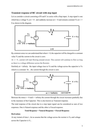
  • 1. yayavaram@yahoo.com 1 Transient response of RC circuit with step input Let us consider a circuit consisting of R and C in series with a Step input. A step signal is one which has a voltage V0 at t < 0 and suddenly increase at t = 0 and remains constant Vs at t >> 0 as shown in the diagram. By common sense we can understand that when t < 0, the capacitor will be charged to a constant value V0 and the current in the circuit is zero. At t = 0 , current will start flowing around circuit. This current will continue to flow as long as there is a voltage difference across the Resistor. Similarly at = infinity the input voltage rises to Vs and the voltage across the capacitor is Vs which is a constant. So , the current through the circuit is zero. Between the times t < 0 and t = infinity the current through the circuit increases gradually due to the reactance of the Capacitor. This is also known as Transient response. The total response of the circuit due to a step input signal can be considered as sum of two responses. One is Natural response and the other is Forced response. Total Response = Natural Response + Forced Response Derivation: At any instant of time t , let us assume that the voltage across the resistor is VR and voltage across the Capacitor is Vc .
  • 2. yayavaram@yahoo.com 2 Then VR= i.R and i = VR /R The same current is passed through the Capacitor also. The current through the Capacitor is i = C 𝑑𝑉 𝑑𝑡 where V is the voltage across the capacitor. From the circuit VR = Vs – V Therefore C 𝑑𝑉 𝑑𝑡 = VR /R = Vs – V 𝑅 C 𝑑𝑉 𝑑𝑡 = Vs 𝑅 - V 𝑅 C 𝑑𝑉 𝑑𝑡 + V 𝑅 = Vs 𝑅 ----------------------------(1) This is a non-homogeneous Equation whose solution consists of two parts. One is Complementary Function part ( i.e natural response at t = 0) and the other is Particular Integral Part(i.e Forced response when t = œ). Natural Response: Natural response of the circuit means, the response of the circuit without any external signal. This circuit is shown below. The voltage across the Capacitor at any instant is given by VN(t) = K.𝑒−𝑡/𝑅𝐶 --------------------------(2) Here RC is called the Time Constant of the RC circuit. It has the units of time (sec) Similarly the forced response means, the response of the circuitwhen external signal is applied . In the present case the external input signal is Step Signal. At t = Infinity, the voltage is equal to Vs . Hence VF(t) = Vs -----------------------------(3) So, the total response is VT = VN(t) + VF(t) So, VT = K.𝑒−𝑡/𝑅𝐶 + Vs To find the value of the constant K ,let us apply the initial conditions .At t = 0 VT = V0 = K + Vs where V0 is the voltage when t =0 Or K = V0 – Vs Hence VT = (V0 – Vs ) 𝒆−𝒕/𝑹𝑪 + Vs
  • 3. yayavaram@yahoo.com 3 This is the total transient response of the RC circuit with Step Input Signal .This is graphically shown as below. Here RC denotes the time constant. Suppose the capacitor is initially discharged, Vo = 0.Sothe the above equation will beome VT = (– Vs) 𝒆−𝒕/𝑹𝑪 + Vs VT = (Vs – Vs ) 𝒆−𝒕/𝑹𝑪 = Vs(1-𝒆−𝒕/𝑹𝑪 ) So the total response of the RC circuit is VT = Vs (1 - 𝒆−𝒕/𝑹𝑪 ) The response of the RC circuit with initially Capacitor discharged is shown in the above diagram. It has both steady state and transient states. Real life applications of RC circuits i. Digital Camera Flash Light utilizes a RC circuit to create a short duration high current pulse to energize the flash light. ii. Neon Lights use RC delay timer circuit for periodic ON/OFF to avoid overheating. iii. On computer mother boards for performing switching operations. --------------XXX--------------
  • 4. yayavaram@yahoo.com 4 Transient response of RL circuit with step input Let us consider a circuit consisting of R and L in series with a Step input signal. A step signal is one which has a voltage V0 at t < 0 and suddenly increase at t = 0 and remains constant Vs at t >> 0 as shown in the diagram. By common sense we can understand that when t < 0, the Inductor current is i0 . At t=0 , current will start flowing around circuit. This current will continue to flow as long as there is a voltage difference across the Resistance. Similarly at t = infinity the input voltage rises to Vs and the voltage across the inductor is Vs which is a constant. The current through the inductor is Is Between the times t < 0 and t = infinity the current through the circuit increases gradually due to the reactance of the Inductor. This is also known as Transient response. The total response of the circuit due to a step input signal can be considered as sum of two responses. One is Natural response and the other is Forced response. Total Response = Natural Response + Forced Response Or Total Response = Transient Response + Steady state Response We know that the transient response is always exponential.
  • 5. yayavaram@yahoo.com 5 So at any instant t , the current through the Inductor is I(t) = i1(t) + i2(t) Where i1(t) = K.𝑒−𝑡𝑅/𝐿 where K is a constant whose value is to be found from initial conditions. Similarly the forced response is (at t = Infinity) i2(t) = Is Hence the complete response is i(t) = i1 + i2 so, I(t) = K.𝑒−𝑡𝑅/𝐿 + Is ------------------ (1) Applying the initial conditions, at t = 0 I(t) = I0 ; So , I0 = K + Is Or K = I0 - Is Substituting in equation 1 I(t) = (I0 -Is ).𝒆−𝒕𝑹/𝑳 + Is So, the Response of a LR circuit for a Step input signal is given by I(t) = (I0 – Is) 𝒆−𝒕𝑹/𝑳 + Is -----------------------------(2) This is the total transient response of the LR circuit with Step Input Signal .This is graphically shown as below. Here L/R denotes the time constant. Suppose the Inductor has no initial current I0 = 0. So the above equation (2) will become I(t) = (0 – Is) 𝒆−𝒕𝑹/𝑳 + Is Or the total response of the RC circuit is I(t) = Is (1 - 𝒆−𝒕𝑹/𝑳 ) This response can be shown graphically as below.
  • 6. yayavaram@yahoo.com 6 The response of the LR circuit with initially Inductor current is zero is shown in the above diagram. It has both steady state and transient states. Real life applications of RL circuits i. RL circuits are used in Relay coils. Relay coil is nothing but an RL circuit used to control the switching of another circuit ii. RL combination is used in Spark plugs of Vehicles to ignite fuel-air mixture in each cylinder at proper times iii. Also used in Fluorescent tubes and single phase motors etc. Frequency Response of RC Circuit (Low Pass Filter) Let us consider a circuit consisting of a Resistor R and a Capacitor C connected in series with a source of AC as shown in the diagram below. The input voltage is Vi and the output voltage is V0. The current in the circuit is I. This circuit can act as a low–pass filter which allows the signals of only low frequency and attenuates the high frequency signals. To analyse the frequency response of the circuit, apply KVL to the circuit.
  • 7. yayavaram@yahoo.com 7 Vi = IR + I.Xc where Xc is the capacitive reactance and I is the total current in the circuit. The capacitive reactance is given by Xc = 1 𝑗𝜔𝐶 So, Vi = I.R + I. 1 𝑗𝜔𝐶 ---------------------------(1) Or Vi = I.(R+1/jωC) I = 𝑉𝑖 ( R+ 1 𝑗𝜔𝐶 ) ----------------------------------(2) From the circuit, the output voltage or voltage across the Capacitor is V0 = I.Xc = 𝑉𝑖 ( R+ 1 𝑗𝜔𝐶 ) .Xc So, V0 = 𝑉𝑖 ( R+ 1 𝑗𝜔𝐶 ) . 1 𝑗𝜔𝐶 Or V0 = 𝑉𝑖 ( 𝑗𝜔𝐶R+1) The gain of the circuit is V0 Vi = 1 ( 𝑗𝜔𝐶R+1) Here ω = 2πF , where F s the frequency of the applied input signal . Let 1 2πRC = Fc be the Cut-off frequency of the RC circuit. So, is V0 Vi = 1 (1+ 𝑗 2πFRC) = 1 (1+ 𝑗. F Fc ) This gain is the complex gain. The magnitude of the gain is given by A = | V0 Vi | = 1 √(1+( . F Fc )2 This equation gives the frequency –Gain response of a CR circuit. This also represents the operation of a Low-pass filter. In the above equation, when the frequency of the applied signal F is small, 1 √(1+( . F Fc )2 = 1 The gain is equal to 1. Or output voltage is equal to input voltage. i.e V0 = Vi which means , the circuit passes low frequency signals completely.
  • 8. yayavaram@yahoo.com 8 When frequency F is large in the term 1 √(1+( . F Fc )2 the denominator is very large or gain is very small. So only very small part of the input is passed through the circuit or the output is almost zero. This response can be shown in the graph below and it is called low-pass filter response. When the frequency of the input signal is equal to cut-off frequency Fc i.e at F = Fc , Gain A = 1 √2 So, the cut-off frequency of the CR circuit can also be defined as the frequency at which the gain becomes to 1 √2 times the maximum value or the output voltage is 0.707 times to the input voltage. This cut-off frequency is also known as 3dB frequency The cut-off Frequency of the RC circuit is Fc = 𝟏 𝟐𝛑𝐑𝐂 The frequencies over which the input signal is totally passed is called pass band and where the gain is minimum is called stop band. RC LOW-PASS FILTER AS PASSIVE INTEGRATOR RC low –pass filter acts as a passive Integrator when the time constant of the circuit is very large. An integrator circuit is one whose output voltage is proportional to the Integral of input Voltage. i.e V0 α ∫ 𝑉𝑖 𝑑𝑡 . Let us consider a circuit consisting of Resistor® and Capacitor ( C ) connected in series with an alternating source of voltage Vi as shown in the below diagram.
  • 9. yayavaram@yahoo.com 9 The important condition is that the time constant (RC) of the circuit is very large. When the time constant is very large, the Capacitor takes more time to charge and hence the entire input voltage appears across Resistor only. Because voltage across the Capacitor will be very small. So, from the circuit Vi = I.R ……………….. (1). and I = 𝑉𝑖 𝑅 ……………….. (2) Now, from the circuit the output voltage across the Capacitor V0 = 𝑄 𝐶 And we know that Q = ∫ 𝐼 𝑑𝑡 Hence V0 = 1 𝐶 ∫ 𝐼 𝑑𝑡 ………………….(3). Substituting (2) in the above equation V0 = 1 𝐶 ∫ 𝑉𝑖 𝑅 𝑑𝑡 Or V0 = 𝟏 𝑹𝑪 ∫ 𝑽𝒊 𝒅𝒕 Hence V0 α ∫ 𝑽𝒊 𝒅𝒕 as R & C are constants. i.e the output voltage is proportional to the integral of input voltage. Hence, a RC low –pass filter circuit with high time constant will act as an Integrator. Frequency Response of CR Circuit (High Pass Filter) Let us consider a circuit consisting of a Capacitor (C) and a Resistor R connected in series with a source of AC as shown in the diagram below. The input voltage is Vi and the output voltage is V0. The current in the circuit is I. This circuit can act as a High –pass filter which allows the signals of only high frequency and attenuates the low frequency signals.
  • 10. yayavaram@yahoo.com 10 To analyse the frequency response of the circuit, apply KVL to the circuit. Vi = IR + I.Xc where Xc is the capacitive reactance and I is the total current in the circuit. The capacitive reactance is given by Xc = 1 𝑗𝜔𝐶 So, Vi = I.R + I. 1 𝑗𝜔𝐶 ------------------------------(1) Or Vi = I. (R+ 1/jωC) I = 𝑉𝑖 ( R+ 1 𝑗𝜔𝐶 ) ------------------------------------(2) From the circuit, the output voltage or voltage across the Resistor R is V0 = I.R = 𝑉𝑖 ( R+ 1 𝑗𝜔𝐶 ) .R So, V0 = 𝑉𝑖 ( R+ 1 𝑗𝜔𝐶 ) 𝑅 . Or V0 = 𝑉𝑖 ( 1+ 1 𝑗𝜔𝐶R ) The gain of the circuit is V0 Vi = 1 ( 1+ 1 𝑗𝜔𝐶R ) Here ω = 2πF, where F s the frequency of the applied input signal. Let 1 2πRC = Fc be the Cut-off frequency of the RC circuit. So, is V0 Vi = 1 (1+ 1/ 𝑗 2πFRC) = 1 (1+ 𝑗. FC F ) This gain is the complex gain. The magnitude of the gain is given by A = | V0 Vi | = 1 √ (1+ . FC F )2 This equation gives the frequency – Gain response of a RC circuit. This also represents the operation of a High-pass filter.
  • 11. yayavaram@yahoo.com 11 In the above equation, when the frequency of the applied signal F is very small, then √ (1+ . FC F )2 = 0 The gain is equal to 0. Or output voltage is equal to 0.i.e the signal is not allowed through the circuit. Or the signal is attenuated. i.e V0 = 0 which means , the circuit do not passes low frequency signals completely. When the when the frequency of the applied signal F is very high, then √ (1+ . FC F )2 = 1 The gain is equal to 1. Or output voltage is equal to Vi. i.e the input signal is completely allowed through the circuit. Or the signal is passed. i.e V0 = Vi which means , the circuit passes high frequency signals completely. This is the working of a High-Pass filter. The response of the CR circuit is shown below. When the frequency of the input signal is equal to cut-off frequency Fc. i.e at F = Fc , Gain A = 1 √2 So, the cut-off frequency of the CR circuit can also be defined as the frequency at which the gain becomes to 1 √2 times the maximum value or the output voltage is 0.707 times to the input voltage. This cut-off frequency is also known as 3dB frequency The cut-off Frequency of the CR circuit is Fc = 𝟏 𝟐𝛑𝐑𝐂 The frequencies over which the input signal is totally passed is called pass band and where the gain is minimum is called stop band.
  • 12. yayavaram@yahoo.com 12 CR HIGH - PASS FILTER AS PASSIVE DIFFERENTIATOR CR High –pass filter acts as a passive differentiator when the time constant of the circuit is very small. A differential circuit is one whose output voltage is proportional to the differential of input Voltage. i.e V0 α 𝑑𝑉𝑖 𝑑𝑡 Let us consider a circuit consisting of Capacitor ( C ) and Resistor (R ) connected in series with an alternating source of voltage Vi as shown in the below diagram. The important condition is that the time constant (RC) of the circuit is very low. When the time constant is very low, the Capacitor takes very less time to charge and hence the entire input voltage appears across Capacitor only when compared to Resistor. As the voltage across the Resistor is very small from the circuit Vi = Q/C ………………..(1). and Q = 𝐶𝑉𝑖 ………………..(2) Now, from the circuit the output voltage across the Resistor R is V0 = IR = R 𝑑𝑄 𝑑𝑡 From equation (2), we know that Q = 𝐶𝑉𝑖 Hence V0 = 𝑅. 𝑑𝐶𝑉𝑖 𝑑𝑡 or V0 = 𝑅𝐶 𝑑𝑉𝑖 𝑑𝑡 … ------------------- (3) therefore V0 α 𝒅𝑽𝒊 𝒅𝒕 as R & C are constants. i.e the output voltage is proportional to the differential of input voltage. Hence, a CR High –pass filter circuit with low time constant can act as a Differentiator.
  • 13. yayavaram@yahoo.com 13 RL LOW - PASS FILTER AS PASSIVE DIFFERENTIATOR RL Low–pass filter acts as a passive differentiator when the time constant of the circuit is very large. A differentia circuit is one whose output voltage is proportional to the differential of input Voltage. i.e V0 α 𝑑𝑉𝑖 𝑑𝑡 Let us consider a circuit consisting of Resistor (R ) & Inductor (L) connected in series with an alternating source of voltage Vi as shown in the below diagram. Since the time constant is very large, the inductor takes more time to build or develop a voltage in it. So, the maximum input voltage will be across the resistor only. So, the input voltage Vi = I R Or I = 𝑉𝑖 𝑅 ………………………….(1) The output voltage or the voltage across the Inductor is V0 = L 𝑑𝐼 𝑑𝑡 ---------------(2) Substituting the value of I from equation (1) V0 = L 𝑑 𝑉𝑖 𝑅 𝑑𝑡 = 𝐿 𝑅 𝑑𝑉𝑖 𝑑𝑡 Since 𝐿 𝑅 , which is the time constant of RL circuit is a constant, it can be written as V0 α 𝑑𝑉𝑖 𝑑𝑡 i.e the output voltage is proportional to the differential of Input voltage .So this circuit acts as a differentiator circuit. L R HIGH - PASS FILTER AS PASSIVE INTEGRATOR LR high –pass filter acts as a passive Integrator when the time constant of the circuit is very small.
  • 14. yayavaram@yahoo.com 14 An integrator circuit is one whose output voltage is proportional to the Integral of input Voltage. i.e V0 α ∫ 𝑉𝑖 𝑑𝑡 . Let us consider a circuit consisting of Inductor (L ) and Resistor ( R ) connected in series with an alternating source of voltage Vi as shown in the below diagram. The important condition is that the time constant (RC) of the circuit is very small. When the time constant is very small, the Inductor takes less time to build or develop the voltage and hence the entire input voltage appears across Inductor only. So, voltage across the Resistor is very small. So, from the circuit Vi = L 𝑑𝐼 𝑑𝑡 ………… ……..(1). and 𝑑𝐼 𝑑𝑡 = 𝑉𝑖 𝐿 dI = 𝑉𝑖 𝐿 .dt or I = ∫ 𝑉𝑖 𝐿 𝑑𝑡 -----------------------------(2) Now, from the circuit the output voltage across the Resistor V0 = I.R And substituting the value of I from the equation (2) V0 = 𝑅. ∫ 𝑉𝑖 𝐿 𝑑𝑡 Or V0 = 𝑅 𝐿 ∫ 𝑉𝑖 𝑑𝑡 As R/L is a constant (Time Constant) of LR circuit we can write the above equation as V0 α ∫ 𝑽𝒊 𝒅𝒕 . i.e the output voltage is proportional to the integral of input voltage. Hence, a LR High –pass filter circuit with small time constant can act as an Integrator. BAND –PASS FILTER (Passive)
  • 15. yayavaram@yahoo.com 15 A band-pass filter is one which allows only a band or group of frequencies and rejects (attenuates) all other frequency signals outside this band. A passive band pass filter can be constructed by cascading (connecting) a High-pass filter with a Low-pass filter s shown in the diagram. Circuit: In the above circuit, the first section (I) acts like a High pass filter with a cut-off frequency of Fc1 and the second section (II) acts like a Low-pass filter with the cut-off frequency Fc2. When the action of both the filters is combined the operation is Band-pass filter. i.e a Band Pass Filters passes signals of certain “band” or “ group” of frequencies without distorting the input signal or adding any extra noise. This band of frequencies is commonly known as the Bandwidth of the Filter. Band-width is also defined as the difference between the upper cut-off frequency and Lower cut-off frequency. BW = Fc2 - Fc1 This type of Band-pass filters are widely used in noise cancellation circuits in communication systems. A band pass filter is considered as a second-order (two-pole) type filter because it has “two” reactive components in its construction. Also, the phase angle will be twice that of the first- order filters, ie, 180o. The frequency response of a Band-pass filter is shown in the graph below.
  • 16. yayavaram@yahoo.com 16 The upper cut-off frequency is Fc2 = 1 2𝜋𝑅2𝐶2 And the lower cut-off Frequency is Fc1 = 1 2𝜋𝑅1𝐶1 The centre frequency is F = √Fc1Fc2 F = √ 1 2𝜋𝑅1𝐶1.2𝜋𝑅2𝐶2 . = 1 2𝜋 1 √𝑅1𝑅2𝐶1𝐶2 Suppose R1=R2=R and C1 = C2 = C The centre Frequency of the Band-pass filter is F = 1 2𝜋 1 √𝑅𝑅𝐶𝐶 = 1 2𝜋𝑅𝐶 So, the centre frequency of the Band-Pass filter is F = 𝟏 𝟐𝝅𝑹𝑪 Time constant of a circuit. Time Constant of a circuit always gives the time response of the circuit when an input voltage or signal is applied. The time constant of any electronic circuit mainly depend on the reactive components (capacitive or inductive) connected in the circuit. The time constant is normally denoted by Tau (τ) with units secs. Time Constant of RC circuit. The time constant of a RC circuit is τ = RC The response of RC circuit is V(t) = V0(1-𝒆−𝒕/𝑹𝑪 ) = V0(1-𝒆−𝒕/τ ) When t = τ V(t) = V0(1- 𝒆−𝟏 ) = V0(1- 0.37) = 0.63V0 (nearly) or Q(t) = Q0(1-𝒆−𝒕/τ ) = 0.63Q0
  • 17. yayavaram@yahoo.com 17 So, the Time constant of a RC circuit can be defined as the time in which the change or voltage on a Capacitor increases to 63% of its maximum value or decays to 37% of the maximum value. Time Constant of RL Circuit The time constant of a RL circuit is τ = L/R The response of RL circuit is V(t) = V0(1-𝒆−𝒕𝑹/𝑳 ) = V0(1-𝒆−𝒕/τ ) or I(t) = I0(1-𝒆−𝒕/τ ) here τ = L/R is the Inductive time constant. When t = τ V(t) = V0(1- 𝒆−𝟏 ) = V0(1- 0.37) = 0.63V0 (nearly) or I(t) = I0(1-𝒆−𝒕/τ ) = 0.63I0 So, the Time constant of a RL circuit can be defined as the time in which the current or voltage on a Inductor increases to 63% of its maximum value or decays to 37% of the maximum value.