FPGA are a special form of Programmable logic devices(PLDs) with higher densities as compared to custom ICs and capable of implementing functionality in a short period of time using computer aided design (CAD) software....by mathewsubin3388@gmail.com
Routing in Integrated circuits is an important task which requires extreme care while placing the modules and circuits and connecting them with each other.
TYPES OF PLACEMENT,GOOD PLACEMENT VS. BAD PLACEMENT ,ALGORITHMS, ASIC DESIGN FLOW DIAGRAM,DEFINITION OF PLACEMENT,TECHNIQUES USED FOR PLACEMENT,PLACEMENT TRENDS,SOLUTIONS
A fundamental introduction to Intellectual Property in VLSI domain. Starts from basics and includes types of IPs and their examples, life cycle of an IP and other few topics in brief in an interactive Q-A manner.
The material is also available at : https://wordpress.com/stats/day/vlsifundamentals.wordpress.com
This presentation gives an overview of FPGA devices. An FPGA is a device that contains a matrix of re-configurable gate array logic circuitry. When a FPGA is configured, the internal circuitry is connected in a way that creates a hardware implementation of the software application.
FPGA devices can deliver the performance and reliability of dedicated hardware circuitry.
A VLSI (Very Large Scale Integration) system integrates millions of “electronic components” in a small area (few mm2 few cm2).
design “efficient” VLSI systems that has:
Circuit Speed ( high )
Power consumption ( low )
Design Area ( low )
An application-specific IC (ASIC) can be either a digital or an analog circuit. As their name implies, ASICs are not reconfigurable; they perform only one specific function. For example, a speed controller IC for a remote control car is hard-wired to do one job and could never become a microprocessor. An ASIC does not contain any ability to follow alternate instructions.
Digital standard cell library Design flowijsrd.com
Commercial library cells are companies 'proprietary information and understandably companies usually impose certain restrictions on the access and use of their library cells. Those restrictions on commercial library cells severely hamper VLSI research and teaching activities of academia. To address the problem the goal of this paper is to discuss the development of standard cell library. This involves in creating new standard cells, layout design, simulation and verification of each standard cell and finally characterization of all cells for timing and functional properties.
In semiconductor design, standard-cell methodology is a method of designing application-specific integrated circuits (ASICs) with mostly digital-logic features. Standard-cell methodology is an example of design abstraction, whereby a low-level very-large-scale integration (VLSI) layout is encapsulated into an abstract logic representation (such as a NAND gate).
Cell-based methodology – the general class to which standard cells belong – makes it possible for one designer to focus on the high-level (logical function) aspect of digital design, while another designer focuses on the implementation (physical) aspect. Along with semiconductor manufacturing advances, standard-cell methodology has helped designers scale ASICs from comparatively simple single-function ICs (of several thousand gates), to complex multi-million gate system-on-a-chip (SoC) devices.
ARM PROCESSOR ARCHITECTURE with reference to ARM state and Thumb state. CPSR register and shift from one state to another ,applications of Thumb and limitations of Thumb.
https://www.youtube.com/watch?v=MW2M6hvAuis
ARM 7 TDMI Processor architecture ,with reference to Processing modes, CPSR Register organization, Privileged and Unprivileged modes are explained.
https://www.youtube.com/watch?v=8oAZEJCwZu8&t=11
8085 Microprocessor Architecture for beginners.It explains the Instruction Register(IR),Instruction Decoder, Address buffer register,Address data buffer,program execution,Serial I/O control etc.
This PPT is about the ARM processors, family of processors,significance,applications and architectural features and Instruction Set Architecture useful for beginners
This is about the 8085 Microprocessor Architecture for absolute beginners.It explains register organization , Temporary registers,General Purpose Registers ,Special Function Registers,Stack Pointer(SP),Program Counter(PC),Stack operation,PUSH, POP operation with examples.
Immunizing Image Classifiers Against Localized Adversary Attacksgerogepatton
This paper addresses the vulnerability of deep learning models, particularly convolutional neural networks
(CNN)s, to adversarial attacks and presents a proactive training technique designed to counter them. We
introduce a novel volumization algorithm, which transforms 2D images into 3D volumetric representations.
When combined with 3D convolution and deep curriculum learning optimization (CLO), itsignificantly improves
the immunity of models against localized universal attacks by up to 40%. We evaluate our proposed approach
using contemporary CNN architectures and the modified Canadian Institute for Advanced Research (CIFAR-10
and CIFAR-100) and ImageNet Large Scale Visual Recognition Challenge (ILSVRC12) datasets, showcasing
accuracy improvements over previous techniques. The results indicate that the combination of the volumetric
input and curriculum learning holds significant promise for mitigating adversarial attacks without necessitating
adversary training.
Industrial Training at Shahjalal Fertilizer Company Limited (SFCL)MdTanvirMahtab2
This presentation is about the working procedure of Shahjalal Fertilizer Company Limited (SFCL). A Govt. owned Company of Bangladesh Chemical Industries Corporation under Ministry of Industries.
About
Indigenized remote control interface card suitable for MAFI system CCR equipment. Compatible for IDM8000 CCR. Backplane mounted serial and TCP/Ethernet communication module for CCR remote access. IDM 8000 CCR remote control on serial and TCP protocol.
• Remote control: Parallel or serial interface.
• Compatible with MAFI CCR system.
• Compatible with IDM8000 CCR.
• Compatible with Backplane mount serial communication.
• Compatible with commercial and Defence aviation CCR system.
• Remote control system for accessing CCR and allied system over serial or TCP.
• Indigenized local Support/presence in India.
• Easy in configuration using DIP switches.
Technical Specifications
Indigenized remote control interface card suitable for MAFI system CCR equipment. Compatible for IDM8000 CCR. Backplane mounted serial and TCP/Ethernet communication module for CCR remote access. IDM 8000 CCR remote control on serial and TCP protocol.
Key Features
Indigenized remote control interface card suitable for MAFI system CCR equipment. Compatible for IDM8000 CCR. Backplane mounted serial and TCP/Ethernet communication module for CCR remote access. IDM 8000 CCR remote control on serial and TCP protocol.
• Remote control: Parallel or serial interface
• Compatible with MAFI CCR system
• Copatiable with IDM8000 CCR
• Compatible with Backplane mount serial communication.
• Compatible with commercial and Defence aviation CCR system.
• Remote control system for accessing CCR and allied system over serial or TCP.
• Indigenized local Support/presence in India.
Application
• Remote control: Parallel or serial interface.
• Compatible with MAFI CCR system.
• Compatible with IDM8000 CCR.
• Compatible with Backplane mount serial communication.
• Compatible with commercial and Defence aviation CCR system.
• Remote control system for accessing CCR and allied system over serial or TCP.
• Indigenized local Support/presence in India.
• Easy in configuration using DIP switches.
CFD Simulation of By-pass Flow in a HRSG module by R&R Consult.pptxR&R Consult
CFD analysis is incredibly effective at solving mysteries and improving the performance of complex systems!
Here's a great example: At a large natural gas-fired power plant, where they use waste heat to generate steam and energy, they were puzzled that their boiler wasn't producing as much steam as expected.
R&R and Tetra Engineering Group Inc. were asked to solve the issue with reduced steam production.
An inspection had shown that a significant amount of hot flue gas was bypassing the boiler tubes, where the heat was supposed to be transferred.
R&R Consult conducted a CFD analysis, which revealed that 6.3% of the flue gas was bypassing the boiler tubes without transferring heat. The analysis also showed that the flue gas was instead being directed along the sides of the boiler and between the modules that were supposed to capture the heat. This was the cause of the reduced performance.
Based on our results, Tetra Engineering installed covering plates to reduce the bypass flow. This improved the boiler's performance and increased electricity production.
It is always satisfying when we can help solve complex challenges like this. Do your systems also need a check-up or optimization? Give us a call!
Work done in cooperation with James Malloy and David Moelling from Tetra Engineering.
More examples of our work https://www.r-r-consult.dk/en/cases-en/
Final project report on grocery store management system..pdfKamal Acharya
In today’s fast-changing business environment, it’s extremely important to be able to respond to client needs in the most effective and timely manner. If your customers wish to see your business online and have instant access to your products or services.
Online Grocery Store is an e-commerce website, which retails various grocery products. This project allows viewing various products available enables registered users to purchase desired products instantly using Paytm, UPI payment processor (Instant Pay) and also can place order by using Cash on Delivery (Pay Later) option. This project provides an easy access to Administrators and Managers to view orders placed using Pay Later and Instant Pay options.
In order to develop an e-commerce website, a number of Technologies must be studied and understood. These include multi-tiered architecture, server and client-side scripting techniques, implementation technologies, programming language (such as PHP, HTML, CSS, JavaScript) and MySQL relational databases. This is a project with the objective to develop a basic website where a consumer is provided with a shopping cart website and also to know about the technologies used to develop such a website.
This document will discuss each of the underlying technologies to create and implement an e- commerce website.
Student information management system project report ii.pdfKamal Acharya
Our project explains about the student management. This project mainly explains the various actions related to student details. This project shows some ease in adding, editing and deleting the student details. It also provides a less time consuming process for viewing, adding, editing and deleting the marks of the students.
Welcome to WIPAC Monthly the magazine brought to you by the LinkedIn Group Water Industry Process Automation & Control.
In this month's edition, along with this month's industry news to celebrate the 13 years since the group was created we have articles including
A case study of the used of Advanced Process Control at the Wastewater Treatment works at Lleida in Spain
A look back on an article on smart wastewater networks in order to see how the industry has measured up in the interim around the adoption of Digital Transformation in the Water Industry.
2. Introduction
• ASIC [“a-sick”] is an acronym for Application
Specific Integrated Circuit.
• As the name indicates, ASIC is a non-standard
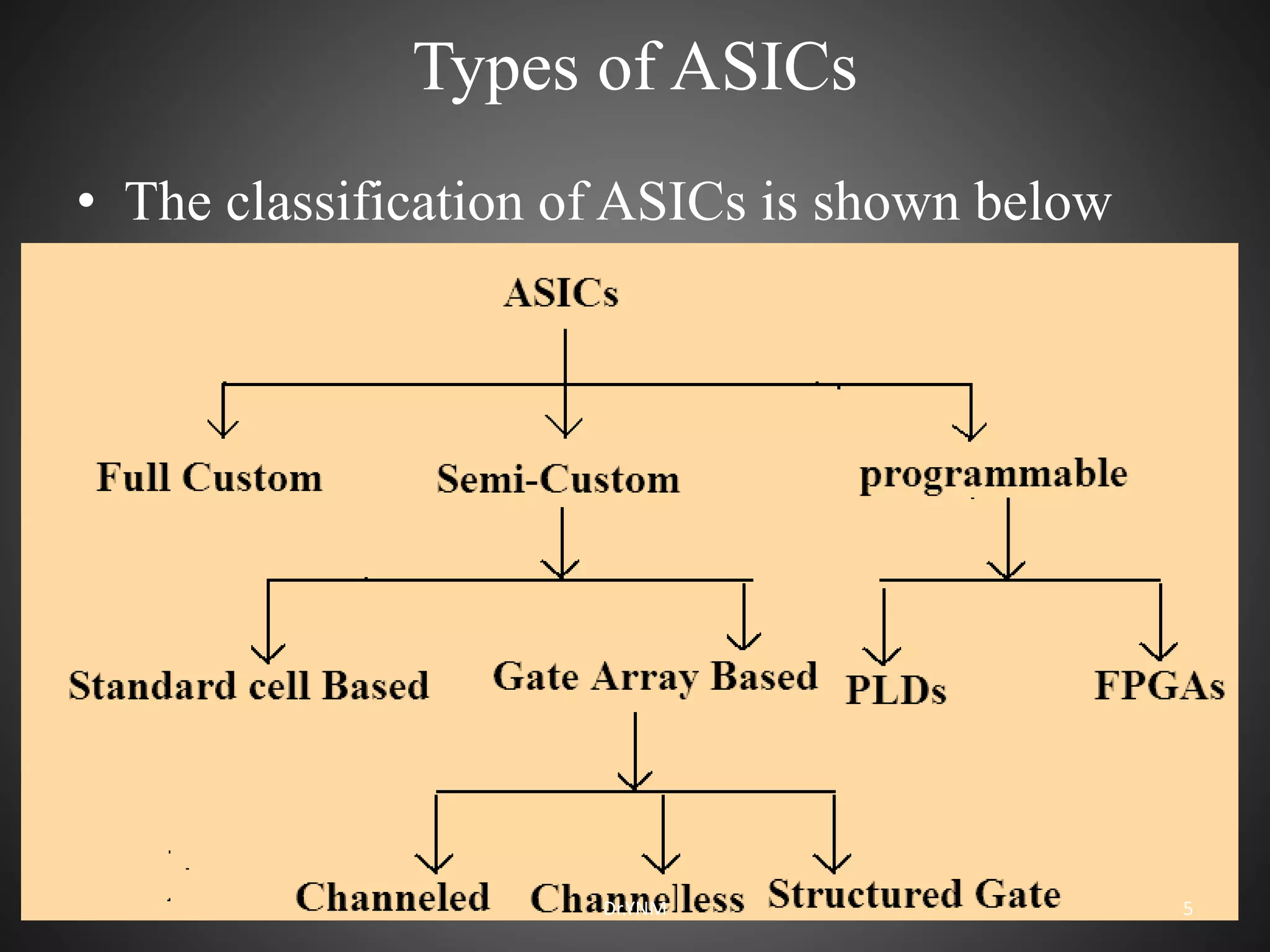
integrated circuit that is designed for a specific
use or application.
• Generally an ASIC design will be undertaken for a
product that will have a large production run , and
the ASIC may contain a very large part of the
electronics needed on a single integrated circuit.
Dr.YNM 2
3. contd..
• Examples for ASIC chips are : a chip for a
toy bear that talks; a chip for a satellite; a
chip designed to handle the interface
between memory and a microprocessor for a
workstation CPU; and a chip containing a
microprocessor as a cell together with other
logic.
Dr.YNM 3
4. contd..
• Two ICs that might or might not be
considered as ASICs are, a controller chip
for a PC and a chip for a modem. Both of
these examples are specific to an application
(shades of an ASIC) but are sold to many
different system vendors (shades of a
standard part). ASICs such as these are
sometimes called application-specific
standard products ( ASSPs ).
Dr.YNM 4
5. Types of ASICs
• The classification of ASICs is shown below
Dr.YNM 5
6. contd..
• So, as shown in the slide the ASICs are
broadly classified into three types.
• I. Full-Custom ASICs
• II. Semi-custom ASICs
• III. Programmable ASICs
Dr.YNM 6
7. Full-Custom ASICs
• A Full custom ASIC is one which includes some
(possibly all) logic cells that are customized and all mask
layers that are customized.
• A microprocessor is an example of a full-custom IC .
Designers spend many hours squeezing the most out of
every last square micron of microprocessor chip space by
hand.
• Customizing all of the IC features in this way allows
designers to include analog circuits, optimized memory
cells, or mechanical structures on an IC, for example.
Full-custom ICs are the most expensive to manufacture
and to design.
Dr.YNM 7
8. Contd..
• The manufacturing lead time (the time
required just to make an IC not including
design time) is typically eight weeks for a
full-custom IC.
• These specialized full-custom ICs are often
intended for a specific application so, we
might call some of them as full-custom
ASICs.
Dr.YNM 8
9. Contd…
• In a full-custom ASIC an engineer designs some
or all of the logic cells, circuits, or layout
specifically for one ASIC. This means the
designer avoids using pretested and pre
characterized cells for all or part of that design.
• This might be because existing cell libraries are
not fast enough, or the logic cells are not small
enough or consume too much power.
Dr.YNM 9
10. contd…
• One has to use full-custom design if the ASIC
technology is new or so specialized that there are
no existing cell libraries or because the ASIC is so
specialized that some circuits must be custom
designed.
• Fewer and fewer full-custom ICs are being
designed because of the problems with these
special parts of the ASIC.
• The growing member of this family, now a days
is , the mixed analog/digital ASIC,
Dr.YNM 10
11. Semicustom ASICs
• ASICs , for which all of the logic cells are
predesigned and some (possibly all) of the mask
layers are customized are called semi custom
ASICs.
• Using the predesigned cells from a cell library
makes the design , much easier.
• There are two types of semicustom ASICs
• (i) Standard-cell–based ASICs (ii)Gate-array–
based ASICs.
Dr.YNM 11
12. Standard-Cell Based ASICs
• A cell-based ASIC (cell-based IC, or CBIC
pronounced sea-bick) uses predesigned logic cells
(AND gates, OR gates, multiplexers, and flip-flops,
for example) known as standard cells.
• One can apply the term CBIC to any IC that uses
cells, but it is generally accepted that a cell-based
ASIC or CBIC means a standard-cell based ASIC.
Dr.YNM 12
13. contd…
• The standard-cell areas (also called flexible blocks)
in a CBIC are built of rows of standard cells like a
wall built of bricks. The standard-cell areas may be
used in combination with microcontrollers or
even microprocessors, known as mega cells.
Mega cells are also called mega functions, full-
custom blocks, system-level macros (SLMs), fixed
blocks, cores, or Functional Standard Blocks
(FSBs).
Dr.YNM 13
14. A cell-based ASIC (CBIC) die with a single
standard-cell area (a flexible block) together with
four fixed blocks.
Dr.YNM 14
15. contd…
• The ASIC designer defines only the placement of the
standard cells and the interconnect in a CBIC.
However, the standard cells can be placed anywhere
on the silicon; this means that all the mask layers of
a CBIC are customized and are unique to a
particular customer.
• The advantage of CBICs is that designers save time,
money, and reduce risk by using a predesigned,
pretested, and pre characterized standard-cell library.
• In addition each standard cell can be optimized
individually. During the design of the cell library
each and every transistor in every standard cell can
be chosen to maximize speed or minimize area .
Dr.YNM 15
16. contd…
• The disadvantages are the time or expense of
designing or buying the standard-cell library
and the time needed to fabricate all layers of
the ASIC for each new design.
Dr.YNM 16
17. Gate-Array Based ASICs
• In a gate array (sometimes abbreviated GA)
or gate-array based ASIC the transistors are
predefined on the silicon wafer.
• The predefined pattern of transistors on a
gate array is the base array , and the smallest
element that is replicated to make the base
array is the base cell (sometimes called a
primitive cell ).
Dr.YNM 17
18. Contd…
• Only the top few layers of metal, which define
the interconnect between transistors, are
defined by the designer using custom masks.
To distinguish this type of gate array from
other types of gate array, it is often called a
masked gate array ( MGA ).
• The designer chooses from a gate-array library
of predesigned and pre-characterized logic
cells
Dr.YNM 18
19. Contd…
• The logic cells in a gate-array library are often
called macros . The reason for this is that the
base-cell layout is the same for each logic cell,
and only the interconnect (inside cells and
between cells) is customized, which is similar
to a software macro.
Dr.YNM 19
20. Types of MGA or Gate-array based ASICs
• There are three types of Gate Array based
ASICs.
• Channeled gate arrays.
• Channelless gate arrays.
• Structured gate arrays.
Dr.YNM 20
21. Channeled gate arrays
• The channeled gate array was the first to be
developed . In a channeled gate array space is
left between the rows of transistors for wiring.
• A channeled gate array is similar to a CBIC.
Both use the rows of cells separated by
channels used for interconnect. One difference
is that the space for interconnect between
rows of cells are fixed in height in a channeled
gate array, whereas the space between rows of
cells may be adjusted in a CBIC.
Dr.YNM 21
23. Features of MGA
• Only the interconnect is customized.
• The interconnect uses predefined spaces
between rows of base cells.
• Manufacturing lead time is between two days
and two weeks.
Dr.YNM 23
24. Channel less Gate Array
• This channel less gate-array architecture is now
more widely used . The routing on a channelless
gate array uses rows of unused transistors.
• The key difference between a channel less gate
array and channeled gate array is that there are
no predefined areas set aside for routing
between cells on a channel less gate array.
Instead we route over the top of the gate-array
devices. We can do this because we customize
the contact layer that defines the connections
between metal 1, the first layer of metal, and
the transistors.
Dr.YNM 24
25. Features of Channel less Gate Array
• Only the interconnect is customized.
• The interconnect uses predefined spaces
between rows of base cells.
• Manufacturing lead time is around two days to
two weeks.
• When we use an area of transistors for routing
in a channel less array, we do not make any
contacts to the devices lying underneath , we
simply leave the transistors unused.
Dr.YNM 25
26. A channel less gate-array or sea-of-gates
(SOG) array die.
Dr.YNM 26
27. Contd…
• The basic difference between a channel less gate
array and channeled gate array is that there are no
predefined areas set aside for routing between cells
on a channel less gate array. Instead we route over the
top of the gate-array devices.
• It is done like this because we customize the contact
layer that defines the connections between metal1, the
first layer of metal, and the transistors. When we use
an area of transistors for routing in a channel less
array, we do not make any contacts to the devices
lying underneath; we simply leave the transistors
unused.
Dr.YNM 27
28. Contd…
• The logic density ,the amount of logic that can be
implemented in a given silicon area is higher for
channel less gate arrays than for channeled gate
arrays. This is usually attributed to the difference in
structure between the two types of array. In fact, the
difference occurs because the contact mask is
customized in a channel less gate array, but is not
usually customized in a channeled gate array. This
leads to denser cells in the channel less architectures.
Customizing the contact layer in a channel less gate
array allows us to increase the density of gate-array
cells because we can route over the top of unused
contact sites.
Dr.YNM 28
29. Structured Gate Array
• This design combines some of the features of CBICs
and MGAs.It is also known as an embedded gate array
or structured gate array(also called as master slice or
master image).
• One of the limitations of the MGA is the fixed gate-
array base cell. This makes the implementation of
memory, difficult and inefficient.
• In an embedded gate array some of the IC area is set
aside and dedicate it to a specific function. This
embedded area either can contain a different base cell
that is more suitable for building memory cells, or it can
contain a complete circuit block, such as a
microcontroller. Dr.YNM 29
30. A structured or embedded gate-array die showing
an embedded block in the upper left corner
Dr.YNM 30
31. Features of Structured Gate Array
• Only the interconnect is customized.
• Custom blocks (the same for each design) can
be embedded.
• Manufacturing lead time is between two days
and two weeks.
• An embedded gate array gives the improved
area efficiency and increased performance of
a CBIC but with the lower cost and faster turn
around of an MGA.
• The disadvantage of an embedded gate array is
that the embedded function is fixed.
Dr.YNM 31
32. Contd…
• For example, if an embedded gate array
contains an area set aside for a 32 k-bit
memory, but we only need a 16 k-bit
memory, then we may have to waste half
of the embedded memory function.
However, this may still be more efficient
and cheaper than implementing a 32 k-bit
memory using macros on a SOG array
Dr.YNM 32
33. Programmable Logic Devices
• Programmable logic devices ( PLDs ) are
standard ICs that are available in standard
configurations.
• However, PLDs may be configured or
programmed to create a part customized to a
specific application, and so they also belong
to the family of ASICs.
• PLDs use different technologies to allow
programming of the device.
Dr.YNM 33
35. Features of PLDs
• No customized mask layers or logic cells
• Fast design turnaround
• A single large block of programmable
interconnect
• A matrix of logic macro cells that usually
consist of programmable array logic followed
by a flip-flop or latch
Dr.YNM 35
36. Contd…
• The simplest type of programmable IC is a
read-only memory( ROM ). The most common
types of ROM use a metal fuse that can be
blown permanently (a programmable ROM or
PROM ).
• An electrically programmable ROM , or
EPROM , uses programmable MOS transistors
whose characteristics are altered by applying a
high voltage.
Dr.YNM 36
37. Contd…
• One can erase an EPROM either by using another
high voltage (an electrically erasable PROM , or
EEPROM ) or by exposing the device to
ultraviolet light (UV-erasable PROM, or
UVPROM).
• There is another type of ROM that can be placed
on any ASIC a mask-programmable ROM (mask-
programmed ROM or masked ROM). A masked
ROM is a regular array of transistors permanently
programmed using custom mask patterns.
• So, an embedded masked ROM is a large,
specialized, logic cell.
Dr.YNM 37
38. Field-Programmable Gate Arrays(FPGAs)
• FPGAs are the newest member of the ASIC family
and are rapidly growing in , replacing TTL in
microelectronic systems. Even though an FPGA is
a type of gate array, we do not consider the term
gate-array based ASICs to include FPGAs.
• There is very little difference between an FPGA
and a PLD .An FPGA is usually just larger and
more complex than a PLD. In fact, some vendors
that manufacture programmable ASICs call their
products as FPGAs and some call them as
complex PLDs .
Dr.YNM 38
39. Characteristics of an FPGA
• None of the mask layers are customized.
• There is a method for programming the basic
logic cells and the interconnect.
• The core is a regular array of programmable basic
logic cells that can implement combinational as
well as sequential logic (flip-flops).
• A matrix of programmable interconnect
surrounds the basic logic cells.
• Programmable I/O cells surround the core.
• Design turnaround is a few hours.
Dr.YNM 39
41. Contd…
• The architecture consists of configurable
logic blocks, configurable I/O blocks, and
programmable interconnect. Also, there
will be clock circuitry for driving the
clock signals to each logic block, and
additional logic resources such as ALUs,
memory, and decoders may be available.
The two basic types of programmable
elements for an FPGA are Static RAM
and anti-fuses.
Dr.YNM 41
42. contd…
Examples of SRAM based FPGA families are
• Altera FLEX family
• Atmel AT6000 and AT40K families
• Lucent Technologies ORCA family
• Xilinx XC4000 and Virtex families
Examples of Anti-fuse based FPGA families are
• Actel SX and MX families
• Quick logic pASIC family
Dr.YNM 42
43. CPLDs vs. FPGAs
CPLD FPGA
• Architecture: PAL-like Gate Array-like
• Density: Low to medium Medium to high
12 22V10s or more up to 1 million gates
• Speed: Fast, predictable Application dependent
• Interconnect: Crossbar Routing
• Power Consumption: High Medium
Dr.YNM 43
44. Design Flow
• The sequence of steps to design an ASIC is known as the
Design flow . The various steps involved in ASIC design
flow are given below.
1. Design entry : Design entry is a stage where the micro
architecture is implemented in a Hardware Description
language like VHDL, Verilog , System Verilog etc.
• In early days , a schematic editor was used for design
entry where designers instantiated gates. Increased
complexity in the current designs require the use of HDLs
to gain productivity . Another advantage is that HDLs are
independent of process technology and hence can be re-
used over time
.
Dr.YNM 44
45. Contd…
2. Logic synthesis: Use an HDL (VHDL or Verilog) and
a logic synthesis tool to produce a net list a description
of the logic cells and their connections
3.System partitioning : Divide a large system into ASIC-
sized pieces.
4. Pre-layout simulation: Check to see if the design
functions correctly.
5. Floor planning: Arrange the blocks of the netlist on
the chip.
6. Placement: Decide the locations of cells in a block.
7. Routing: Make the connections between cells and
blocks.
Dr.YNM 45
46. Contd…
8.Extraction : Determine the resistance and
capacitance of the interconnect.
9. Post layout simulation. It is used to check to
see whether the design still works with the
added loads of the interconnect or not
The flow diagram is shown in the next slide.
Dr.YNM 46
48. Contd…
• In the flow diagram the steps from 1 to 4 are
part of logical design ,and steps from 5 to 9 are
part of physical design.
• When we are performing system partitioning
we have to consider both logical and physical
factors.
Dr.YNM 48
49. CMOS Design Rules
• The design rules are Interface between
designer and process engineer and guidelines
for constructing process masks
• The figures in the next slides defines the
design rules for a CMOS process using
pictures. Arrows between objects denote a
minimum spacing, and arrows showing the
size of an object denote a minimum width.
Rule 3.1, for example, is the minimum width
of poly (2 l ).
Dr.YNM 49
52. Contd…
• Dimensions are in l . Rule numbers are in
parentheses (missing rule sets 11 to 13 are
extensions to this basic process)
• Each of the rule numbers may have different
values for different manufacturers there are
no standards for design rules
Dr.YNM 52