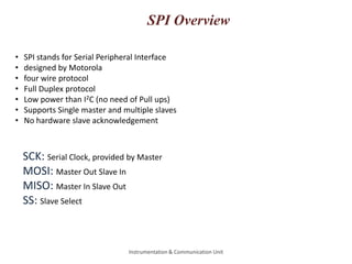
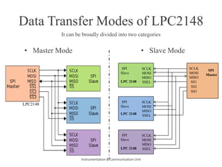
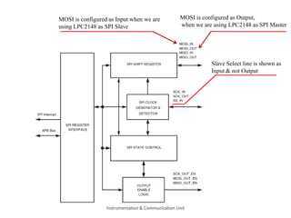
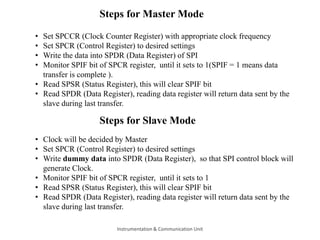
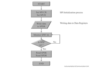
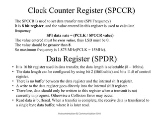
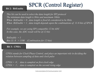
SPI Protocol in LPC2148
By- Dnyanesh P. Joshi
Instrumentation & Communication Unit
SPI Overview
SCK: Serial Clock, provided by Master
MOSI: Master Out Slave In
MISO: Master In Slave Out
SS: Slave Select
• SPI stands for Serial Peripheral Interface
• designed by Motorola
• four wire protocol
• Full Duplex protocol
• Low power than I2C (no need of Pull ups)
• Supports Single master and multiple slaves
• No hardware slave acknowledgement
Instrumentation & Communication Unit
Data Transfer Modes of LPC2148
It can be broadly divided into two categories
• Master Mode • Slave Mode
LPC2148
SPI
Slave
SCLK
MOSI
MISO
SSEL
SPI
Slave
SCLK
MOSI
MISO
SSEL
SPI
Slave
SCLK
MOSI
MISO
SSELLPC 2148
LPC 2148
LPC 2148
SCLK
MOSI
MISO
SS1
SS2
SS3
SPI
Master
Instrumentation & Communication Unit
Slave Select line is shown as
Input & not Output
MOSI is configured as Input when we are
using LPC2148 as SPI Slave
MOSI is configured as Output,
when we are using LPC2148 as SPI Master
Instrumentation & Communication Unit
• Set SPCCR (Clock Counter Register) with appropriate clock frequency
• Set SPCR (Control Register) to desired settings
• Write the data into SPDR (Data Register) of SPI
• Monitor SPIF bit of SPCR register, until it sets to 1(SPIF = 1 means data
transfer is complete ).
• Read SPSR (Status Register), this will clear SPIF bit
• Read SPDR (Data Register), reading data register will return data sent by the
slave during last transfer.
Steps for Master Mode
• Clock will be decided by Master
• Set SPCR (Control Register) to desired settings
• Write dummy data into SPDR (Data Register), so that SPI control block will
generate Clock.
• Monitor SPIF bit of SPCR register, until it sets to 1
• Read SPSR (Status Register), this will clear SPIF bit
• Read SPDR (Data Register), reading data register will return data sent by the
slave during last transfer.
Steps for Slave Mode
Instrumentation & Communication Unit
START
Set SPCCR
Set SPCR
Monitor SPIF bit
Write data
to SPDR
Is SPIF
set ?
Read SPSR
Read SPDR
END
No
Yes
SPI Initialization process
Writing data to Data Registers
Instrumentation & Communication Unit
Clock Counter Register (SPCCR)
The SPCCR is used to set data transfer rate (SPI Frequency)
It is 8 bit register, and the value entered in this register is used to calculate
frequency
SPI data rate = (PCLK / SPCCR value)
The value entered must be even value, thus LSB must be 0.
The value should be greater than 8.
So maximum frequency is 1.875 MHz(PCLK = 15MHz).
Data Register (SPDR)
• It is 16 bit register used in data transfer, the data length is selectable (8 – 16bits).
• The data length can be configured by using bit 2 (BitEnable) and bits 11:8 of control
register.
• There is no buffer between the data register and the internal shift register.
• A write to the data register goes directly into the internal shift register.
• Therefore, data should only be written to this register when a transmit is not
currently in progress. Otherwise a Collision Error may occur.
• Read data is buffered. When a transfer is complete, the receive data is transferred to
a single byte data buffer, where it is later read.
Instrumentation & Communication Unit
SPCR (Control Register)
This bit can be used to select the data length for SPI protocol
The minimum data length is 8bits and maximum 16bits
When BitEnable = 0 , data length is fixed & considered to be 8bits
When BitEnable = 1 , data length depends upon the combinations of 11:8 bits of SPCR
For example, we are using SPI compatible 12 bit ADC
In this case, the ADC result will be of 12 bits
BitEnable = 1
Bits 11: 8 = 1100 (Combination for 12 bits)
CPHA stands for Clock Phase Control, and plays an important role in deciding the
relation between sampling of data and clock pulse
CPHA = 0 ; data is sampled on first clock edge
CPHA = 1 ; data is sampled on the second rising edge
Bit 3: CPHA
Bit 2: BitEnable
Instrumentation & Communication Unit
• The important thing to be considered here is CPHA should be 0 when LPC2148 is used
as a SPI Master.
• It is mentioned in the User Manual of LPC2148 that SSEL signal is inactive during the
data transfer when CPHA is 0, but when CPHA is 1 the SSEL signal becomes active
and immediately transforms itself into slave.
• This results into a Mode Fault and data transfer terminates.
• In this case MODF bit of Status Register will set to 1.
• CPOL stands for Clock Polarity Control
• The bit decides the polarity of SPI clock, when set to 1 clock is active low. In that case
• first clock will start with negative going pulse
• when set to 0 the clock is active high meaning that the clock will start with positive
• going edge
CPOL = 0
CPOL = 1
Bit 4: CPOL
Instrumentation & Communication Unit
• The bit is used to configure SPI block in Master/Slave Mode
• MSTR = 0 Slave Mode
• MSTR = 1 Master Mode
Bit 5: MSTR
• The bit decides the direction of bit transfer
• LSBF = 0 MSB is transferred first
• LSBF = 1 LSB is transferred first
Bit 6: LSBF
• It is an interrupt Enable bit,
• SPIE = 0 Interrupt are disabled
• SPIE = 1 Interrupts are enabled and will occur when SPI/ WCOL bit is set
Bit 7: SPIE
Instrumentation & Communication Unit
When bit 2 of this register is 1, this field controls the number of bits per transfer:
1000 8 bits per transfer
1001 9 bits per transfer
1010 10 bits per transfer
1011 11 bits per transfer
1100 12 bits per transfer
1101 13 bits per transfer
1110 14 bits per transfer
1111 15 bits per transfer
0000 16 bits per transfer
Bit 11:8 BITS
Example: The target device is 12bit ADC, which is slave and LPC2148 is Master
Bit 0 1 2 3 4 5 6 7 8 9 10 11
- - 1 0 0 1 0 0 1 1 0 0
Control Register (SPCR)
Instrumentation & Communication Unit
Some Imp points…
a read or write of the SPI data register is required in order to clear the SPIF status bit.
The prime function of SPSR register is to indicate the completion of data transfer
between two devices. The remaining bits of SPSR register
When CPHA = 0, the SSEL signal will always go inactive between data
transfers. This is not guaranteed when CPHA = 1 (the signal can remain active). (pg
169)
Instrumentation & Communication Unit
Thank You !!!
Instrumentation & Communication Unit

SPI Protocol in LPC2148

  • 1.
    SPI Protocol inLPC2148 By- Dnyanesh P. Joshi Instrumentation & Communication Unit
  • 2.
    SPI Overview SCK: SerialClock, provided by Master MOSI: Master Out Slave In MISO: Master In Slave Out SS: Slave Select • SPI stands for Serial Peripheral Interface • designed by Motorola • four wire protocol • Full Duplex protocol • Low power than I2C (no need of Pull ups) • Supports Single master and multiple slaves • No hardware slave acknowledgement Instrumentation & Communication Unit
  • 3.
    Data Transfer Modesof LPC2148 It can be broadly divided into two categories • Master Mode • Slave Mode LPC2148 SPI Slave SCLK MOSI MISO SSEL SPI Slave SCLK MOSI MISO SSEL SPI Slave SCLK MOSI MISO SSELLPC 2148 LPC 2148 LPC 2148 SCLK MOSI MISO SS1 SS2 SS3 SPI Master Instrumentation & Communication Unit
  • 4.
    Slave Select lineis shown as Input & not Output MOSI is configured as Input when we are using LPC2148 as SPI Slave MOSI is configured as Output, when we are using LPC2148 as SPI Master Instrumentation & Communication Unit
  • 5.
    • Set SPCCR(Clock Counter Register) with appropriate clock frequency • Set SPCR (Control Register) to desired settings • Write the data into SPDR (Data Register) of SPI • Monitor SPIF bit of SPCR register, until it sets to 1(SPIF = 1 means data transfer is complete ). • Read SPSR (Status Register), this will clear SPIF bit • Read SPDR (Data Register), reading data register will return data sent by the slave during last transfer. Steps for Master Mode • Clock will be decided by Master • Set SPCR (Control Register) to desired settings • Write dummy data into SPDR (Data Register), so that SPI control block will generate Clock. • Monitor SPIF bit of SPCR register, until it sets to 1 • Read SPSR (Status Register), this will clear SPIF bit • Read SPDR (Data Register), reading data register will return data sent by the slave during last transfer. Steps for Slave Mode Instrumentation & Communication Unit
  • 6.
    START Set SPCCR Set SPCR MonitorSPIF bit Write data to SPDR Is SPIF set ? Read SPSR Read SPDR END No Yes SPI Initialization process Writing data to Data Registers Instrumentation & Communication Unit
  • 7.
    Clock Counter Register(SPCCR) The SPCCR is used to set data transfer rate (SPI Frequency) It is 8 bit register, and the value entered in this register is used to calculate frequency SPI data rate = (PCLK / SPCCR value) The value entered must be even value, thus LSB must be 0. The value should be greater than 8. So maximum frequency is 1.875 MHz(PCLK = 15MHz). Data Register (SPDR) • It is 16 bit register used in data transfer, the data length is selectable (8 – 16bits). • The data length can be configured by using bit 2 (BitEnable) and bits 11:8 of control register. • There is no buffer between the data register and the internal shift register. • A write to the data register goes directly into the internal shift register. • Therefore, data should only be written to this register when a transmit is not currently in progress. Otherwise a Collision Error may occur. • Read data is buffered. When a transfer is complete, the receive data is transferred to a single byte data buffer, where it is later read. Instrumentation & Communication Unit
  • 8.
    SPCR (Control Register) Thisbit can be used to select the data length for SPI protocol The minimum data length is 8bits and maximum 16bits When BitEnable = 0 , data length is fixed & considered to be 8bits When BitEnable = 1 , data length depends upon the combinations of 11:8 bits of SPCR For example, we are using SPI compatible 12 bit ADC In this case, the ADC result will be of 12 bits BitEnable = 1 Bits 11: 8 = 1100 (Combination for 12 bits) CPHA stands for Clock Phase Control, and plays an important role in deciding the relation between sampling of data and clock pulse CPHA = 0 ; data is sampled on first clock edge CPHA = 1 ; data is sampled on the second rising edge Bit 3: CPHA Bit 2: BitEnable Instrumentation & Communication Unit
  • 9.
    • The importantthing to be considered here is CPHA should be 0 when LPC2148 is used as a SPI Master. • It is mentioned in the User Manual of LPC2148 that SSEL signal is inactive during the data transfer when CPHA is 0, but when CPHA is 1 the SSEL signal becomes active and immediately transforms itself into slave. • This results into a Mode Fault and data transfer terminates. • In this case MODF bit of Status Register will set to 1. • CPOL stands for Clock Polarity Control • The bit decides the polarity of SPI clock, when set to 1 clock is active low. In that case • first clock will start with negative going pulse • when set to 0 the clock is active high meaning that the clock will start with positive • going edge CPOL = 0 CPOL = 1 Bit 4: CPOL Instrumentation & Communication Unit
  • 10.
    • The bitis used to configure SPI block in Master/Slave Mode • MSTR = 0 Slave Mode • MSTR = 1 Master Mode Bit 5: MSTR • The bit decides the direction of bit transfer • LSBF = 0 MSB is transferred first • LSBF = 1 LSB is transferred first Bit 6: LSBF • It is an interrupt Enable bit, • SPIE = 0 Interrupt are disabled • SPIE = 1 Interrupts are enabled and will occur when SPI/ WCOL bit is set Bit 7: SPIE Instrumentation & Communication Unit
  • 11.
    When bit 2of this register is 1, this field controls the number of bits per transfer: 1000 8 bits per transfer 1001 9 bits per transfer 1010 10 bits per transfer 1011 11 bits per transfer 1100 12 bits per transfer 1101 13 bits per transfer 1110 14 bits per transfer 1111 15 bits per transfer 0000 16 bits per transfer Bit 11:8 BITS Example: The target device is 12bit ADC, which is slave and LPC2148 is Master Bit 0 1 2 3 4 5 6 7 8 9 10 11 - - 1 0 0 1 0 0 1 1 0 0 Control Register (SPCR) Instrumentation & Communication Unit
  • 12.
    Some Imp points… aread or write of the SPI data register is required in order to clear the SPIF status bit. The prime function of SPSR register is to indicate the completion of data transfer between two devices. The remaining bits of SPSR register When CPHA = 0, the SSEL signal will always go inactive between data transfers. This is not guaranteed when CPHA = 1 (the signal can remain active). (pg 169) Instrumentation & Communication Unit
  • 13.
    Thank You !!! Instrumentation& Communication Unit