Downloaded 4,449 times


![Dr.Y.Narasimha MurthyPh.D
yayavaram@yahoo.com
Swap.
Single-Register Transfer : These instructions are used for moving a single data item in and out of a
register. The data types supported are signed and unsigned words (32-bit), half-words (16-bit), and
bytes. Ex1: STR r0, [r1] ; = STR r0, [r1, #0] ; store the contents of register r0 to the
memory address pointed to by register r1.
Ex2 : LDR r0, [r1] ; = LDR r0, [r1, #0] ; load register r0 with the contents of the
memory address pointed to by register r1.
Multiple-Register Transfer : Load-store multiple instructions can transfer multiple registers
between memory and the processor in a single instruction. The transfer occurs from a base
address register Rn pointing into memory. Multiple-register transfer instructions are more
efficient than single-register transfers for moving blocks of data around memory and saving and
restoring context and stacks.
Load-store multiple instructions can increase interrupt latency. ARM implementations do not
usually interrupt instructions while they are executing. For example, on an ARM7 a load
multiple instruction takes 2 + N.t cycles, where N is the number of registers to load and t is the
number of cycles required for each sequential access to memory. If an interrupt has been raised,
then it has no effect until the load-store multiple instruction is complete.
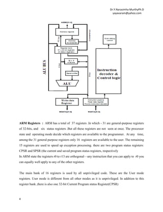
Example 1: LDMIA r0!, {r1-r3} ; In this example, register r0 is the base register Rn and is
followed by !, indicating that the register is updated after the instruction is executed. In this case
the range is from register r1 to r3.
Example 2 : LDMIB : load multiple and increment before
Ex 3: LDMIB r0!, {r1-r3} ;
Ex 4 : LDMDA r0!, {r1-r3}
15](https://image.slidesharecdn.com/unitii-armarchitecture-130305014346-phpapp01/85/ARM7-ARCHITECTURE-15-320.jpg)
![Dr.Y.Narasimha MurthyPh.D
yayavaram@yahoo.com
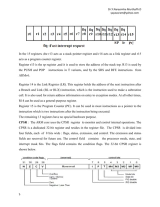
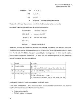
PRE r1 = 0x00000002
r4 = 0x00000003
sp = 0x00080010
STMED sp! , {r1,r4} ; Store Multiple Empty Descending Stack
POST r1 = 0x00000002
r4 = 0x00000003
sp = 0x00080008
This operation is explained in the following figure.
Swap Instruction :
The Swap instruction is a special case of a load-store instruction. It swaps (Similar to exchange)
the contents of memory with the contents of a register. This instruction is an atomic operation—
it reads and writes a location in the same bus operation, preventing any other instruction from
reading or writing to that location until it completes.Swap cannot be interrupted by any other
instruction or any other bus access. So, the system ―holds the bus‖ until the transaction is
complete.
Ex 1: SWP : Swap a word between memory and a register tmp = mem32[Rn]
mem32[Rn] =Rm
Rd = tmp
Ex2 : SWPB Swap a byte between memory and a register tmp = mem8[Rn]
mem8[Rn] =Rm
17](https://image.slidesharecdn.com/unitii-armarchitecture-130305014346-phpapp01/85/ARM7-ARCHITECTURE-17-320.jpg)
![Dr.Y.Narasimha MurthyPh.D
yayavaram@yahoo.com
Rd = tmp.
Ex 3: SWP r0, r1, [r2] ; The swap instruction loads a word from memory into register
r0 and overwrites the memory with register r1.
Software Interrupt Instruction : A software interrupt instruction (SWI) is used to generate a
software interrupt exception, which can be used to call operating system routines.When the
processor executes an SWI instruction, it sets the program counter pc to the offset 0x8 in the
vector table. The instruction also forces the processor mode to SVC, which allows an operating
system routine to be called in a privileged mode. Each SWI instruction has an associated SWI
number, which is used to represent a particular function call or feature.
Ex: 0x00008000 SWI 0x123456
Here 0x123456, is the SWI number used by ARM toolkits as a debugging SWI. Typically
the SWI instruction is executed in user mode.
Program Status Register Instructions : There are two instructions available to directly control
a program status register (PSR). The MRS instruction transfers the contents of either the CPSR
or SPSR into a register.Similarly the MSR instruction transfers the contents of a register into
the CPSR or SPSR .These instructions together are used to read and write the CPSR and
SPSR.
MRS : copy program status register to a general-purpose register , Rd= PSR
MSR : move a general-purpose register to a program status register, PSR[field]=Rm
MSR : move an immediate value to a program status register, PSR[field]=immediate
Ex : MRS r1, CPSR
BIC r1, r1, #0x80 ; 0b01000000
MSR CPSR_C, r1.
The MSR first copies the CPSR into register r1. The BIC instruction clears bit 7 of r1. Register
r1 is then copied back into the CPSR, which enables IRQ interrupts. Here the code preserves all
the other settings in the CPSR intact and only modifies the I bit in the control field.
18](https://image.slidesharecdn.com/unitii-armarchitecture-130305014346-phpapp01/85/ARM7-ARCHITECTURE-18-320.jpg)
![Dr.Y.Narasimha MurthyPh.D
yayavaram@yahoo.com
Loading Constants : In ARM instruction set there are no instructions to move the 32-bit
constant into a register. Since ARM instructions are 32 bits in size, they obviously cannot
specify a general 32-bit constant. To overcome this problem .two pseudo instructions are
provided to move a 32-bit value into a register.
LDR : load constant pseudo instruction Rd= 32-bit constant.
ADR : load address pseudo instruction Rd=32-bit relative address.
The first pseudo instruction writes a 32-bit constant to a register using whatever instructions are
available.
The second pseudo instruction writes a relative address into a register, which will be encoded
using a PC -relative expression.
Example 2: LDR r0, [pc, #constant_number-8-{PC}]
constant _number DCD 0xff00ffff.
Here the LDR instruction loads a 32-bit constant 0xff00ffff into register r0.
Example 3: The same constant can be loaded into the register r0 using the MVN instruction also.
MVN r0, #0x00ff0000
After execution r0 = 0xff00ffff.
Introduction to Thumb instruction set : Thumb encodes a subset of the 32-bit ARM
instructions into a 16-bit instruction set space. Since Thumb has higher performance than ARM
on a processor with a 16-bit data bus, but lower performance than ARM on a 32-bit data bus, use
Thumb for memory-constrained systems. Thumb has higher code density—the space taken up in
memory by an executable program—than ARM. For memory-constrained embedded systems,
for example, mobile phones and PDAs, code density is very important. Cost pressures also limit
memory size, width, and speed.
Thumb execution is flagged by the T bit (bit [5] ) in the CPSR. A Thumb implementation of the
same code takes up around 30% less memory than the equivalent ARM implementation. Even
though the Thumb implementation uses more instructions ; the overall memory footprint is
reduced. Code density was the main driving force for the Thumb instruction set. Because it was
also designed as a compiler target, rather than for hand-written assembly code. Below example
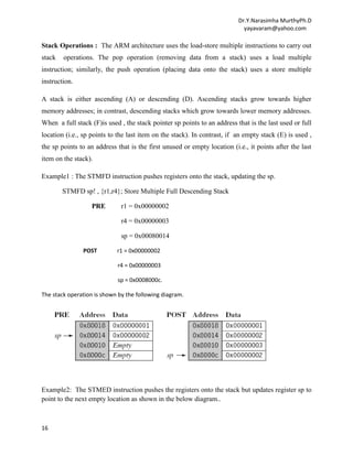
explains the difference between ARM and Thumb code
19](https://image.slidesharecdn.com/unitii-armarchitecture-130305014346-phpapp01/85/ARM7-ARCHITECTURE-19-320.jpg)
![Dr.Y.Narasimha MurthyPh.D
yayavaram@yahoo.com
Form the above discussion, it is clear that there are no MSR and MRS equivalent Thumb
instructions. To alter the CPSR or SPSR , one must switch into ARM state to use MSR and
MRS. Similarly, there are no coprocessor instructions in Thumb state. You need to be in ARM
state to access the coprocessor for configuring cache and memory management.
ARM-Thumb interworking is the method of linking ARM and Thumb code together for both
assembly and C/C++. It handles the transition between the two states. To call a Thumb routine
from an ARM routine, the core has to change state. This is done with the T bit of CPSR . The
BX and BLX branch instructions cause a switch between ARM and Thumb state while branching
to a routine. The BX lr instruction returns from a routine, also with a state switch if necessary.
The data processing instructions manipulate data within registers. They include move
instructions, arithmetic instructions, shifts, logical instructions, comparison instructions, and
multiply instructions. The Thumb data processing instructions are a subset of the ARM data
processing instructions.
Exs : ADC : add two 32-bit values and carry Rd = Rd + Rm + C flag
ADD : add two 32-bit values Rd = Rn + immediate
Rd = Rd + immediate
Rd = Rd + Rm
AND : logical bitwise AND of two 32-bit values Rd = Rd & Rm
ASR : arithmetic shift right Rd = Rm_immediate,
C flag= Rm[immediate − 1]
Rd = Rd_Rs, C flag = Rd[Rs - 1]
BIC : logical bit clear (AND NOT) of two 32-bit Rd = Rd AND
NOT(Rm)values
CMN : compare negative two 32-bit values Rn + Rm sets flags
CMP : compare two 32-bit integers Rn−immediate sets flags Rn−Rm sets flags
EOR : logical exclusive OR of two 32-bit values Rd = Rd EOR Rm
LSL : logical shift left Rd = Rm_ immediate,
C flag= Rm[32 − immediate]
Rd = Rd_Rs, C flag = Rd[32 − Rs]
LSR : logical shift right Rd = Rm_ immediate,
C flag = Rd [immediate − 1]
Rd = Rd_ Rs, C flag = Rd[Rs − 1]
MOV : move a 32-bit value into a register Rd = immediate
21](https://image.slidesharecdn.com/unitii-armarchitecture-130305014346-phpapp01/85/ARM7-ARCHITECTURE-21-320.jpg)
![Dr.Y.Narasimha MurthyPh.D
yayavaram@yahoo.com
Rd = Rn
Rd = Rm
MUL : multiply two 32-bit values Rd = (Rm * Rd)[31:0]
MVN : move the logical NOT of a 32-bit value into a register Rd = NOT(Rm)
NEG : negate a 32-bit value Rd = 0 − Rm
ORR : logical bitwise OR of two 32-bit values Rd = Rd OR Rm
ROR : rotate right a 32-bit value Rd = Rd RIGHT_ROTATE Rs,
C flag= Rd[Rs−1]
SBC : subtract with carry a 32-bit value Rd = Rd − Rm − NOT(C flag)
SUB : subtract two 32-bit values Rd = Rn − immediate
Rd = Rd − immediate
Rd = Rn − Rm
sp = sp − (immediate_2)
TST : test bits of a 32-bit value Rn AND Rm sets flags
Note : Thumb deviates from the ARM style in that the barrel shift operations (ASR, LSL, LSR,
and ROR) are separate instructions.
Thankful to the following people for their invaluable information .
References : 1. ARM System Developer’s Guide Designing and Optimizing System Software –
Andrew N. Sloss , Dominic Symes and Chris Wright.
2. ARM-System on-Chip Architecture – Steve Furber.
3. ARM Architecture Reference Manual Copyright © 1996-1998, 2000, 2004, 2005
ARM Limited.
22](https://image.slidesharecdn.com/unitii-armarchitecture-130305014346-phpapp01/85/ARM7-ARCHITECTURE-22-320.jpg)

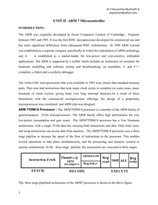
The document provides an overview of the ARM microcontroller architecture, specifically focusing on the ARM7TDMI-S processor, which features a three-stage pipeline and a von Neumann architecture. It discusses the various instruction sets, processor modes, and the significance of registers, including the 31 general-purpose registers and the program status register. The document also details the ARM processor families, highlighting their performance improvements and architectural differences over time.