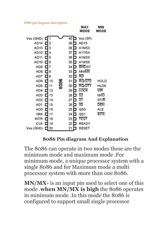
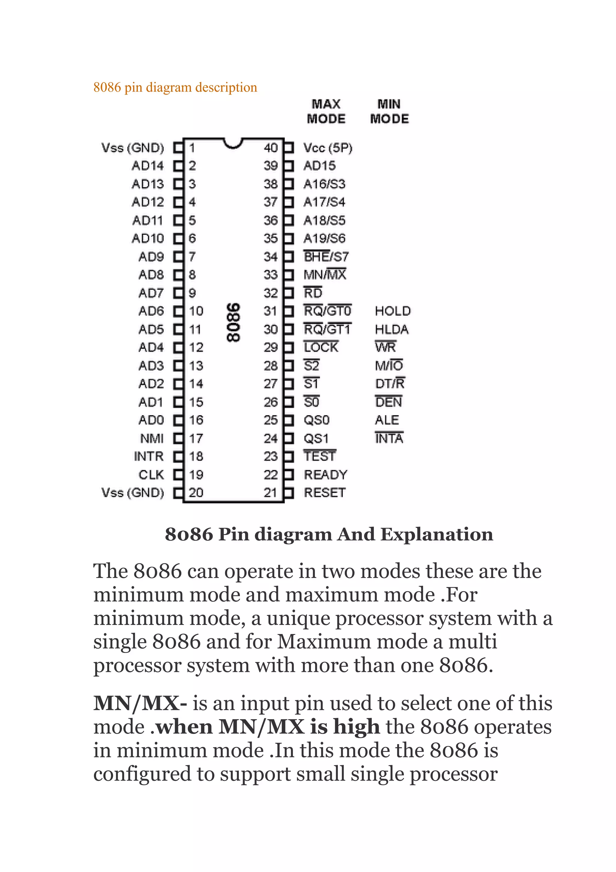
The document describes the pins of the 8086 microprocessor. It operates in either minimum or maximum mode depending on the state of the MN/MX pin. The AD0-AD15 pins are used for the lower 16-bits of addressing or data. The upper 4 address lines are multiplexed with status signals. The BHE/S7 pin is used for bus high enable during instruction execution.
1. 8086 pin diagram description
8086 Pin diagram And Explanation
The 8086 can operate in two modes these are the
minimum mode and maximum mode .For
minimum mode, a unique processor system with a
single 8086 and for Maximum mode a multi
processor system with more than one 8086.
MN/MX- is an input pin used to select one of this
mode .when MN/MX is high the 8086 operates
in minimum mode .In this mode the 8086 is
configured to support small single processor
2. system using a few devices that the system bus
.when MN/MX is low 8086 is configured to
support multiprocessor system.
The AD0-AD15 lines are a 16bit multiplexed
addressed or data bus. During the 1st clock cycle
AD0-AD15 are the low order 16Bit adders. The
8086 has a total of 20 address line ,the upper 4
lines are multiplexed with the state signal that
is A16/S3 , A17/S4 , A18/S5 , A19 /S6.During
the first clock period of a best cycle the entire 20bit
address is available on these line. During all other
clock cycles for memory and i/o operations AD15-
AD0 contain the 16 bit data
andS3,S4,S5,S6 become the status line .S3 and S4
are decoded as follows
A17/S4 A16/S3 Function
0 0 Extra Segment
0 1 Stack Segment
1 0 code or No segment
1 1 Data Segment
There for the 1st clock cycle of an instruction
execution the A17/S4 And A16/S3 pins Specify
which Segment register generate the segment
portions of the 8086 address
3. BHE/S7 is used as best high enable during the
1st click cycle of an instruction execution .the BHE
can be used in conjunction with AD0 to select the
memory
RD is low when the data is read from memory or
I/O location .
TEST is an input pin and is only used by the wait
instruction .the 8086 enter a wait state after
execution of the wait instruction until a low is Sean
on the test pin.
INTR is a maskable interrupt input.
NIM is the non maskable interrupt input.
RESET is the system set reset input signal it
terminates all the activities it
clear PSW,IP,DS,SS,ES and the instruction
Queue.
DT/R(Data Transmit or receive ):is an o/p signal
required in system that uses the data bus
transceiver
ALE is an address latch enable . Is an o/p
signal provided by the 8086 and can be used to
demultiplexed AD0 to AD15 in to A10 toA15 and
D0 to D15.
M/IO is an 8086 output signal to distinguish a
memory access and i/o access.
4. WR is used by the 8086 for performing write
memory or write i/o operation .
INTA(interrupt acknowledgement signal )
INTA is the interrupt acknowledgment signal
HOLD and HOLDA
a high on the HOLD pin indicates that another
master is required to take over the S/M bus
CLK clock provides the basic timing signals for the
8086 and bus controls .
-->