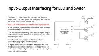
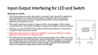
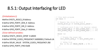
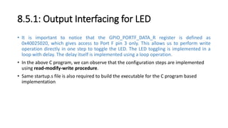
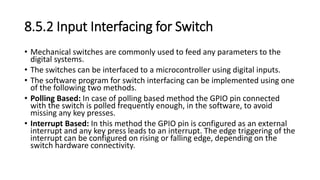
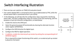
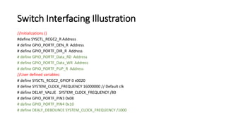
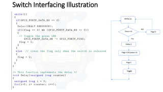
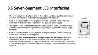
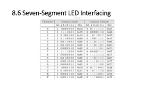
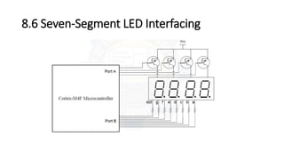
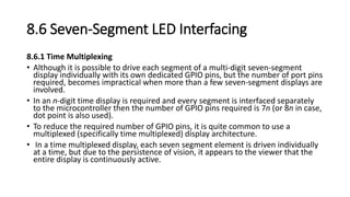
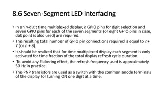
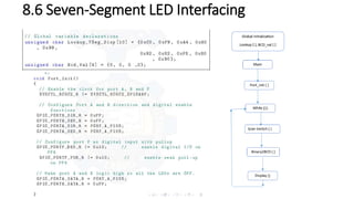
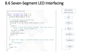
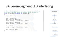
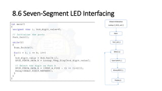
Mechanical switches are commonly used to feed any parameters to the digital systems.
The switches can be interfaced to a microcontroller using digital inputs.
The software program for switch interfacing can be implemented using one of the following two methods
2. Input-Output Interfacing for LED and Switch
• The TM4C123 microcontroller platform has three on
board color LEDs (red, green and blue) and two switches
for simple input output interfacing.
• Both LEDs and switches are interfaced as digital devices.
• In the following, we will learn to interface each of these
two different types of devices.
• LEDs will be interfaced using GPIO pins as digital outputs
and switches will be connected by configuring the GPIO
pins as digital inputs.
• From Figure 8.10, we observe that the LEDs are
connected using digital NPN transistors.
• A digital transistor is the one that integrates the base
(bias) resistors inside the transistor package. Unlike an
ordinary transistor, a digital transistor operate in only two
states, off and saturation.
3. Input-Output Interfacing for LED and Switch
Working of a switch:
• This is true because, when the switch is pressed, logic low will be applied to
the GPIO port pin connected to the switch. However, when the switch is
released, there is no source (or supply) connection to ensure logic high
appears at the GPIO port pin.
• The switch interfacing shown in Figure 8.10 is not complete. With simple
microcontrollers, the switch interface of Figure 8.10 might not work properly.
• However, in case of TM4C123 the above-mentioned problem is resolved by
using the internal pull-up resistor.
• When the internal pull-up resistor is enabled, it pulls the GPIO pin to logic
high when the switch is in released state.
• The internal pull-up resistor values are in general larger than 10kQ. Since the
current drawn by the GPIO port pin, when configured as input, is so low that
the voltage drop across the pull-up resistor is almost negligible and voltage
level, approximately equal to the supply voltage, appears at the GPIO pin,
which is translated as logic high by the internal logic.
4. Input-Output Interfacing for LED and Switch
• A second option, different from the one shown in Figure 8.10, is to change
the switch terminal connection from ground to supply (Vcc).
• For this case we need to enable internal pull-down resistor for proper switch
functioning.
• In this case, logic high will be read by the user program, when the switch is
pressed.
5. 8.5.1: Output Interfacing for LED
For LED interfacing we need to configure Port F pins 1, 2 and 3 as outputs. The basic steps to
configure the required Port F pins are given below.
1. Enable the clock to the GPIO port.
2. Select the general purpose IO functionality by clearing the alternate function select register
(GPIOAFSEL).
3. Configure the GPIO direction for digital output function.
4. Configure the PAD for the digital operation.
7. 8.5.1: Output Interfacing for LED
• It is important to notice that the GPIO_PORTF_DATA_R register is defined as
0x40025020, which gives access to Port F pin 3 only. This allows us to perform write
operation directly in one step to toggle the LED. The LED toggling is implemented in a
loop with delay. The delay itself is implemented using a loop operation.
• In the above C program, we can observe that the configuration steps are implemented
using read-modify-write procedure.
• Same startup.s file is also required to build the executable for the C program based
implementation
8. 8.5.2 Input Interfacing for Switch
• Mechanical switches are commonly used to feed any parameters to the
digital systems.
• The switches can be interfaced to a microcontroller using digital inputs.
• The software program for switch interfacing can be implemented using one
of the following two methods.
• Polling Based: In case of polling based method the GPIO pin connected
with the switch is polled frequently enough, in the software, to avoid
missing any key presses.
• Interrupt Based: In this method the GPIO pin is configured as an external
interrupt and any key press leads to an interrupt. The edge triggering of the
interrupt can be configured on rising or falling edge, depending on the
switch hardware connectivity.
9. 8.5.2 Input Interfacing for Switch
• Before we proceed further, it is important to first familiarize our
self with the switch physical behavior.
• Next we describe the switch bouncing, which is one of the
critical attributes of its physical behavior.
• Electrical switches that use mechanical contacts to close or
open a circuit are subject to bouncing of the contacts
• Switch contacts are usually made of springy metals. When the
contacts strike together, their momentum and elasticity act
together to cause them to bounce one or more times before
making steady contact.
• It results in a pulsating electric signal instead of a clean
transition.
• For a microcontroller GPIO pin configured as input, this switch
bouncing can be interpreted as multiple switch presses.
• Figure 8.11 shows the bouncing of a switch with normally open
contact and is captured using digital storage oscilloscope.
10. 8.5.2 Input Interfacing for Switch
• Both hardware as well as software solutions exist to get around the switch bouncing
problem.
Hardware solution:
• Analog filtering using an RC delay to filter out the rapid changes in switch output can be used
as hardware solution.
• The design task is to choose R and C such that the input threshold is not crossed while
bouncing is still occurring.
Software solution:
In case of software solution to the switch bouncing problem, at the beginning of polling the
switch is checked for being pressed.
If the switch is detected as pressed, then a delay (corresponding to switch denouncing interval)
is inserted and the switch is checked again for being pressed.
If the switch is detected as pressed again, we declare that the switch is pressed.
The rate at which the switch should be polled has to be fast enough that no switch press is
missed, i.e., the time gap between two consecutive switch presses is larger than the scan cycle
duration.
11. Switch Interfacing Illustration
• There are two user switches on TM4C123 evaluation board
• User switch labeled SW1 is connected to Port F pin 4 (abbreviated as PF4), while the
second switch SW2 is connected to Port F pin 0 (PF0).
• In the following, we will describe the configuration steps required for interfacing
switch SW1. The basic configuration steps are similar to the LED interfacing, with the
exception of port pin direction configuration, as listed below:
1. Enable the clock to the GPIO port.
2. Select the general purpose IO functionality by clearing the alternate function
select register (GPIOAFSEL).
3. Configure the GPIO direction for digital input.
4. Configure the PAD for digital operation.
5. In addition, enable the internal pull-up resistor by setting the corresponding bit of
GPIOPUR register.
This is required for proper functioning of the switch, as no external pull-up resistor
is placed on the board.
12. Switch Interfacing Illustration
• The C program illustration for interfacing the switch using polling method is provided in Example
8.4.
• The implementation is such that on every switch press an on board LED (green color) connected
to PF3 will be toggled, which helps to visualize the proper functioning of the switch.
• The LED toggling on switch press can be implemented in two different ways.
• One possible approach is to toggle the LED, as soon as the switch is pressed and the next toggling
of the LED only happens once the switch is first released and then pressed again. This approach
can be termed as edge based LED toggling.
• In the second approach, if the switch is pressed then the LED is toggled and the next LED toggling
happens after some predetermined delay if the switch is still pressed. This approach can be
termed as level based LED toggling.
16. Switch Interfacing Illustration
• The value of the constant DEALY_DEBOUNCE depends on the switch characteristics. For many
switches a debouncing delay of few milliseconds would be sufficient.
• If the flag variable is not used by the program, then the resulting implementation will be
equivalent to level based LED toggling.
17. 8.6 Seven-Segment LED Interfacing
• The seven-segment display is one of the widely used displays that can display
decimal, hexadecimal and in some cases special characters.
• Each of the seven LEDs in the display is called a segment, since when it is
illuminated, it constructs a segment of the digit, to be displayed.
• The eighth LED is used for the indication of a decimal point, (DP) and is used
when two or more seven-segment displays are put together to display larger
numbers.
• Each of the seven LEDs in the segment is assigned a label from a through g
based on its position in the segment.
• In addition, one of the LED pins is brought out of the package for external
connection, while all other terminals of the LEDs are connected together
internally and brought out as single common pin. The common pin is also used
to identify the type of the seven-segment display as common anode or common
cathode
18. 8.6 Seven-Segment LED Interfacing
Common cathode:
In this display type, all cathode terminals of the LED
segments are joined together and are connected to
logic low or ground. While based on the number to
be displayed a collection of individual segments are
illuminated by applying logic high though a current
limiting resistor.
Common anode: In this display type, the
connections are reversed. The common terminal is
of anode type and is connected with logic high, while
individual segment pins are connected to logic low
selectively based on the desired digit to be
displayed.
21. 8.6 Seven-Segment LED Interfacing
8.6.1 Time Multiplexing
• Although it is possible to drive each segment of a multi-digit seven-segment
display individually with its own dedicated GPIO pins, but the number of port pins
required, becomes impractical when more than a few seven-segment displays are
involved.
• In an n-digit time display is required and every segment is interfaced separately
to the microcontroller then the number of GPIO pins required is 7n (or 8n in case,
dot point is also used).
• To reduce the required number of GPIO pins, it is quite common to use a
multiplexed (specifically time multiplexed) display architecture.
• In a time multiplexed display, each seven segment element is driven individually
at a time, but due to the persistence of vision, it appears to the viewer that the
entire display is continuously active.
22. 8.6 Seven-Segment LED Interfacing
• In an n-digit time multiplexed display, n GPIO pins for digit selection and
seven GPIO pins for each of the seven segments (or eight GPIO pins in case,
dot point is also used) are required.
• The resulting total number of GPIO pin connections required is equal to n+
7 (or n + 8).
• It should be realized that for time multiplexed display each segment is only
activated for time fraction of the total display refresh cycle duration.
• To avoid any flickering effect, the refresh frequency used is approximately
50 Hz in practice.
• The PNP transistors are used as a switch with the common anode terminals
of the display for turning ON one digit at a time.