Download to read offline


![contd
CJNE [...], DJNZ [...], JB, JNB, JC, JNC, JBC,
JZ, JNZ – With these conditional branching
instructions the same rule above applies.
Again, violating the memory boundaries may
cause erratic execution.
Dr.YNM 31](https://image.slidesharecdn.com/atmel-230228170801-9e0e7e0b/85/Atmel-ppt-31-320.jpg)


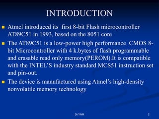
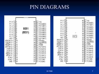
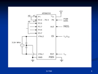
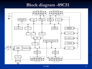
The document discusses Atmel's 8-bit microcontrollers, the AT89C51 and AT89C2051. It provides details on their features such as flash memory size, I/O ports, operating modes, and applications. The AT89C51 was Atmel's first flash microcontroller based on the 8051 core with 4KB flash. The AT89C2051 has 2KB flash, an on-chip analog comparator, and supports power saving modes. Both microcontrollers are compatible with the 8051 instruction set.