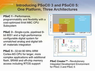
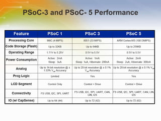
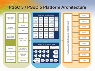
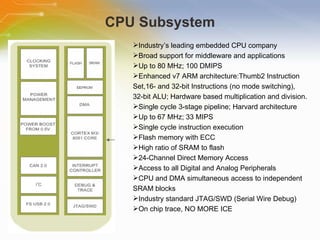
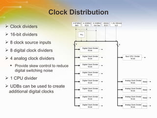
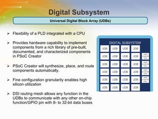
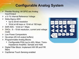
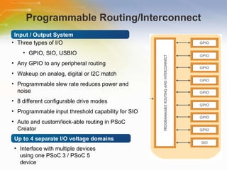
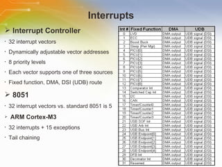
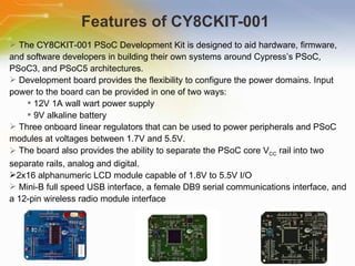
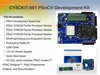
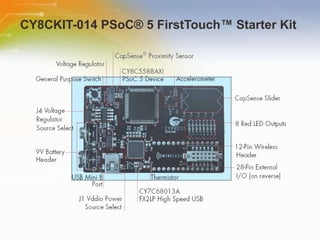
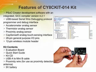
An Overview on Programmable System on Chip: PSoC-5  Source: Cypress Semiconductor
Introduction Purpose An   Overview   on   Programmable   System   on   Chip:   PSoC-5 Outline Introducing   PSoC®   3   and   PSoC®   5 PSoC-3   and   PSoC-   5   Performance CPU   Subsystem,   Digital   and   Analog Interrupts,   Low   Power   Modes PSoC   Creator   Design   Flow PSoC   5   Kits:   CY8CKIT-001,   CY8CKIT-014 Content 20   pages
Introducing PSoC® 3 and PSoC® 5: One Platform, Three Architectures PSoC Creator™ -  Revolutionary Integrated Development Environment for PSoC 3 and PSoC 5 PSoC 1 -  Performance, programmability and flexibility with a cost-optimized 8-bit M8C CPU Subsystem PSoC 3 -  Single-cycle, pipelined 8-bit 8051 and a high-performance configurable digital system for unmatched analog and digital bill-of- materials integration PSoC 5 -  32-bit 80 MHz ARM Cortex-M3 CPU for larger, more complex applications with additional flash, SRAM and off-chip memory access including RTOS support
PSoC-3 and PSoC- 5 Performance
PSoC 3 / PSoC 5 Platform Architecture
CPU Subsystem Industry’s leading embedded CPU company Broad support for middleware and applications Up to 80 MHz; 100 DMIPS Enhanced v7 ARM architecture:Thumb2 Instruction  Set,16- and 32-bit Instructions (no mode switching),  32-bit ALU; Hardware based multiplication and division. Single cycle 3-stage pipeline; Harvard architecture Up to 67 MHz; 33 MIPS Single cycle instruction execution Flash memory with ECC High ratio of SRAM to flash 24-Channel Direct Memory Access Access to all Digital and Analog Peripherals CPU and DMA simultaneous access to independent  SRAM blocks Industry standard JTAG/SWD (Serial Wire Debug) On chip trace, NO MORE ICE
Clock Distribution Clock dividers 16-bit dividers 8 clock source inputs 8 digital clock dividers 4 analog clock dividers Provide skew control to reduce  digital switching noise 1 CPU divider UDBs can be used to create additional digital clocks Digital Clock Divider 16 - bit Digital Clock Divider 16 - bit Digital Clock Divider 16 - bit Digital Clock Divider 16 - bit Digital Clock Divider 16 - bit Digital Clock Divider 16 - bit Digital Clock Divider 16 - bit Digital Clock Divider 16 - bit Analog Clock Divider 16 - bit Analog Clock Divider 16 - bit Analog Clock Divider 16 - bit Analog Clock Divider 16 - bit Skew Skew Skew Skew Bus / CPU  Divider 16 - bit 7 7 PLL 4 - 33 MHz ECO 32 kHz ECO 3 - 67 MHz  IMO 0 - 33 MHz Ext Osc 1 , 33 , 100 kHz  ILO
Digital Subsystem Flexibility of a PLD integrated with a CPU Provides hardware capability to implement components from a rich library of pre-built, documented, and characterized components in PSoC Creator PSoC Creator will synthesize, place, and route components automatically. Fine configuration granularity enables high silicon utilization DSI routing mesh allows any function in the UDBs to communicate with any other on-chip function/GPIO pin with 8- to 32-bit data buses Universal Digital Block Array (UDBs)
Optimized 16-bit Timer/Counter/PWM Blocks Provides nearly all of the features of a UDB based timer, counter, or PWM PSoC Creator provides easy access to these flexible blocks Each block may be configured as either a full featured 16-bit Timer, Counter, or PWM Programmable options Clock, enable, reset, capture, kill from  any pin or digital signal on chip Independent control of terminal count, interrupt, compare, reset, enable, capture, and kill synchronization Plus Configurable to measure pulse widths or periods Buffered PWM with dead band and kill
Configurable Analog System Flexible Routing: All GPIO are Analog Input/Output ±  0.1% Internal Reference Voltage Delta-Sigma ADC:  Up to 20-bit resolution 16-bit at 48 ksps or 12-bit at 192 ksps SAR ADC:  12-bit at 1 Msps DACs:  8 – 10-bit resolution, current and voltage mode Low Power Comparators Op-amps (25 mA output buffers) Programmable Analog Blocks Configurable PGA (up to x50), Mixer, Trans-Impedance Amplifier, Sample and Hold Digital Filter Block: Implement HW IIR and FIR filters CapSense Touch Sensing enabled
Programmable Routing/Interconnect Input / Output System Three types of I/O GPIO, SIO, USBIO Any GPIO to any peripheral routing Wakeup on analog, digital or I2C match Programmable slew rate reduces power and noise 8 different configurable drive modes Programmable input threshold capability for SIO Auto and custom/lock-able routing in PSoC Creator Up to 4 separate I/O voltage domains Interface with multiple devices using one PSoC 3 / PSoC 5 device
Interrupts Interrupt Controller 32 interrupt vectors Dynamically adjustable vector addresses 8 priority levels Each vector supports one of three sources Fixed function, DMA, DSI (UDB) route 8051 32 interrupt vectors vs. standard 8051 is 5 ARM Cortex-M3 32 interrupts + 15 exceptions Tail chaining
Low Power Modes Power mode Current (PSoC 3) Current (PSoC 5) Code execution Digital resources available Analog resources available Clock sources available Wakeup sources Reset sources Active 1.2 mA  @ 6MHz 2 mA  @ 6MHz Yes All All All N/A All Sleep 1 uA 2 uA No I2C Comparator Low Speed and 32 kHz Osc IO, I2C, RTC, sleep timer, comparator XRES, LVD, WDR Hibernate 200 nA 300 nA No None None None IO XRES, LVD Power Management Enabled in PSoC Creator Provides easy to use control APIs for quick power management Allows code and register manipulation for in-depth control
Dedicated Communication Peripherals Full Speed USB device 8 bi-directional data end points + 1 control end point No external crystal required Drivers in PSoC Creator for HID class devices Full CAN 2.0b 16 RX buffers and 8 TX buffers I2C Master or Slave Data rate up to 400 kbps Additional I2C slaves may be implemented in UDB array New peripherals will be added as family members are added to the platform: Ethernet, HS USB, USB Host.
PSoC Creator Design Flow Configure Start a new project Place components Configure components Connect components Develop Build hardware design and  Generate component APIs Write application code utilizing  Component APIs Compile, build and program Debug Perform in-circuit debug using PSoC Creator Reuse Capture working hardware/software designs as your own components for future use
Features   of   CY8CKIT-001   The   CY8CKIT-001   PSoC   Development   Kit   is   designed   to   aid   hardware,   firmware,   and   software   developers   in   building   their   own   systems   around   Cypress’s   PSoC,   PSoC3,   and   PSoC5   architectures. Development   board   provides   the   flexibility   to   configure   the   power   domains.   Input   power   to   the   board   can   be   provided   in   one   of   two   ways:   12V   1A   wall   wart   power   supply 9V   alkaline   battery Three   onboard   linear   regulators   that   can   be   used   to   power   peripherals   and   PSoC   modules   at   voltages   between   1.7V   and   5.5V.   The   board   also   provides   the   ability   to   separate   the   PSoC   core   V CC   rail   into   two   separate   rails,   analog   and   digital.   2x16   alphanumeric   LCD   module   capable   of   1.8V   to   5.5V   I/O   Mini-B   full   speed   USB   interface,   a   female   DB9   serial   communications   interface,   and   a   12-pin   wireless   radio   module   interface
CY8CKIT-001 PSoC® Development Kit  The   kit   contains:   PSoC   Development   Board   test   PSoC   CY8C28   Family   Processor   Module   PSoC   CY8C38   Family   Processor   Module PSoC   CY8C55   Family   Processor   Module MiniProg3   Debug   and   Evaluation   Device   Prototyping   Cable   Kit   USB   Cable   12V   AC   Power   Adapter   Quick   Start   Guide   Kit   CDs,   which   includes:   PSoC   Creator™,   PSoC   Designer™,   PSoC   Programmer,   Projects,   and   Documentation
CY8CKIT-014 PSoC® 5 FirstTouch™ Starter Kit
Features   of   CY8CKIT-014   Kit   PSoC   Creator   development   software   with   an   integrated,   GCC   compiler   version   4.2.1 USB-based   Serial   Wire   Debugging   protocol   programmer   and   debug   interface Accelerometer   analog   sensor Thermistor   analog   sensor Proximity   analog   sensor CapSense®   analog   touch-sensing   interface 28-pin   general   purpose   I/O   pins 12-pin   wireless   module   header Kit   Contents Evaluation   Board Quick   Start   Guide Kit   CD USB   A   to   Mini   B   cable Proximity   wire   (for   use   as   proximity   detection   antenna) 9V   battery
Additional Resource For ordering PSoC 5 devices, please click the part list or Call our sales hotline For more product information go to http://www.cypress.com/?id=2233&source=header Visit Element 14 to post your question   www.element-14.com For additional inquires contact our technical service hotline or even use our “Live Technical Chat” online facility Newark Farnell

An Overview on Programmable System on Chip: PSoC-5

  • 1.
    An Overview onProgrammable System on Chip: PSoC-5 Source: Cypress Semiconductor
  • 2.
    Introduction Purpose An Overview on Programmable System on Chip: PSoC-5 Outline Introducing PSoC® 3 and PSoC® 5 PSoC-3 and PSoC- 5 Performance CPU Subsystem, Digital and Analog Interrupts, Low Power Modes PSoC Creator Design Flow PSoC 5 Kits: CY8CKIT-001, CY8CKIT-014 Content 20 pages
  • 3.
    Introducing PSoC® 3and PSoC® 5: One Platform, Three Architectures PSoC Creator™ - Revolutionary Integrated Development Environment for PSoC 3 and PSoC 5 PSoC 1 - Performance, programmability and flexibility with a cost-optimized 8-bit M8C CPU Subsystem PSoC 3 - Single-cycle, pipelined 8-bit 8051 and a high-performance configurable digital system for unmatched analog and digital bill-of- materials integration PSoC 5 - 32-bit 80 MHz ARM Cortex-M3 CPU for larger, more complex applications with additional flash, SRAM and off-chip memory access including RTOS support
  • 4.
    PSoC-3 and PSoC-5 Performance
  • 5.
    PSoC 3 /PSoC 5 Platform Architecture
  • 6.
    CPU Subsystem Industry’sleading embedded CPU company Broad support for middleware and applications Up to 80 MHz; 100 DMIPS Enhanced v7 ARM architecture:Thumb2 Instruction Set,16- and 32-bit Instructions (no mode switching), 32-bit ALU; Hardware based multiplication and division. Single cycle 3-stage pipeline; Harvard architecture Up to 67 MHz; 33 MIPS Single cycle instruction execution Flash memory with ECC High ratio of SRAM to flash 24-Channel Direct Memory Access Access to all Digital and Analog Peripherals CPU and DMA simultaneous access to independent SRAM blocks Industry standard JTAG/SWD (Serial Wire Debug) On chip trace, NO MORE ICE
  • 7.
    Clock Distribution Clockdividers 16-bit dividers 8 clock source inputs 8 digital clock dividers 4 analog clock dividers Provide skew control to reduce digital switching noise 1 CPU divider UDBs can be used to create additional digital clocks Digital Clock Divider 16 - bit Digital Clock Divider 16 - bit Digital Clock Divider 16 - bit Digital Clock Divider 16 - bit Digital Clock Divider 16 - bit Digital Clock Divider 16 - bit Digital Clock Divider 16 - bit Digital Clock Divider 16 - bit Analog Clock Divider 16 - bit Analog Clock Divider 16 - bit Analog Clock Divider 16 - bit Analog Clock Divider 16 - bit Skew Skew Skew Skew Bus / CPU Divider 16 - bit 7 7 PLL 4 - 33 MHz ECO 32 kHz ECO 3 - 67 MHz IMO 0 - 33 MHz Ext Osc 1 , 33 , 100 kHz ILO
  • 8.
    Digital Subsystem Flexibilityof a PLD integrated with a CPU Provides hardware capability to implement components from a rich library of pre-built, documented, and characterized components in PSoC Creator PSoC Creator will synthesize, place, and route components automatically. Fine configuration granularity enables high silicon utilization DSI routing mesh allows any function in the UDBs to communicate with any other on-chip function/GPIO pin with 8- to 32-bit data buses Universal Digital Block Array (UDBs)
  • 9.
    Optimized 16-bit Timer/Counter/PWMBlocks Provides nearly all of the features of a UDB based timer, counter, or PWM PSoC Creator provides easy access to these flexible blocks Each block may be configured as either a full featured 16-bit Timer, Counter, or PWM Programmable options Clock, enable, reset, capture, kill from any pin or digital signal on chip Independent control of terminal count, interrupt, compare, reset, enable, capture, and kill synchronization Plus Configurable to measure pulse widths or periods Buffered PWM with dead band and kill
  • 10.
    Configurable Analog SystemFlexible Routing: All GPIO are Analog Input/Output ± 0.1% Internal Reference Voltage Delta-Sigma ADC: Up to 20-bit resolution 16-bit at 48 ksps or 12-bit at 192 ksps SAR ADC: 12-bit at 1 Msps DACs: 8 – 10-bit resolution, current and voltage mode Low Power Comparators Op-amps (25 mA output buffers) Programmable Analog Blocks Configurable PGA (up to x50), Mixer, Trans-Impedance Amplifier, Sample and Hold Digital Filter Block: Implement HW IIR and FIR filters CapSense Touch Sensing enabled
  • 11.
    Programmable Routing/Interconnect Input/ Output System Three types of I/O GPIO, SIO, USBIO Any GPIO to any peripheral routing Wakeup on analog, digital or I2C match Programmable slew rate reduces power and noise 8 different configurable drive modes Programmable input threshold capability for SIO Auto and custom/lock-able routing in PSoC Creator Up to 4 separate I/O voltage domains Interface with multiple devices using one PSoC 3 / PSoC 5 device
  • 12.
    Interrupts Interrupt Controller32 interrupt vectors Dynamically adjustable vector addresses 8 priority levels Each vector supports one of three sources Fixed function, DMA, DSI (UDB) route 8051 32 interrupt vectors vs. standard 8051 is 5 ARM Cortex-M3 32 interrupts + 15 exceptions Tail chaining
  • 13.
    Low Power ModesPower mode Current (PSoC 3) Current (PSoC 5) Code execution Digital resources available Analog resources available Clock sources available Wakeup sources Reset sources Active 1.2 mA @ 6MHz 2 mA @ 6MHz Yes All All All N/A All Sleep 1 uA 2 uA No I2C Comparator Low Speed and 32 kHz Osc IO, I2C, RTC, sleep timer, comparator XRES, LVD, WDR Hibernate 200 nA 300 nA No None None None IO XRES, LVD Power Management Enabled in PSoC Creator Provides easy to use control APIs for quick power management Allows code and register manipulation for in-depth control
  • 14.
    Dedicated Communication PeripheralsFull Speed USB device 8 bi-directional data end points + 1 control end point No external crystal required Drivers in PSoC Creator for HID class devices Full CAN 2.0b 16 RX buffers and 8 TX buffers I2C Master or Slave Data rate up to 400 kbps Additional I2C slaves may be implemented in UDB array New peripherals will be added as family members are added to the platform: Ethernet, HS USB, USB Host.
  • 15.
    PSoC Creator DesignFlow Configure Start a new project Place components Configure components Connect components Develop Build hardware design and Generate component APIs Write application code utilizing Component APIs Compile, build and program Debug Perform in-circuit debug using PSoC Creator Reuse Capture working hardware/software designs as your own components for future use
  • 16.
    Features of CY8CKIT-001 The CY8CKIT-001 PSoC Development Kit is designed to aid hardware, firmware, and software developers in building their own systems around Cypress’s PSoC, PSoC3, and PSoC5 architectures. Development board provides the flexibility to configure the power domains. Input power to the board can be provided in one of two ways: 12V 1A wall wart power supply 9V alkaline battery Three onboard linear regulators that can be used to power peripherals and PSoC modules at voltages between 1.7V and 5.5V. The board also provides the ability to separate the PSoC core V CC rail into two separate rails, analog and digital. 2x16 alphanumeric LCD module capable of 1.8V to 5.5V I/O Mini-B full speed USB interface, a female DB9 serial communications interface, and a 12-pin wireless radio module interface
  • 17.
    CY8CKIT-001 PSoC® DevelopmentKit The kit contains: PSoC Development Board test PSoC CY8C28 Family Processor Module PSoC CY8C38 Family Processor Module PSoC CY8C55 Family Processor Module MiniProg3 Debug and Evaluation Device Prototyping Cable Kit USB Cable 12V AC Power Adapter Quick Start Guide Kit CDs, which includes: PSoC Creator™, PSoC Designer™, PSoC Programmer, Projects, and Documentation
  • 18.
    CY8CKIT-014 PSoC® 5FirstTouch™ Starter Kit
  • 19.
    Features of CY8CKIT-014 Kit PSoC Creator development software with an integrated, GCC compiler version 4.2.1 USB-based Serial Wire Debugging protocol programmer and debug interface Accelerometer analog sensor Thermistor analog sensor Proximity analog sensor CapSense® analog touch-sensing interface 28-pin general purpose I/O pins 12-pin wireless module header Kit Contents Evaluation Board Quick Start Guide Kit CD USB A to Mini B cable Proximity wire (for use as proximity detection antenna) 9V battery
  • 20.
    Additional Resource Forordering PSoC 5 devices, please click the part list or Call our sales hotline For more product information go to http://www.cypress.com/?id=2233&source=header Visit Element 14 to post your question www.element-14.com For additional inquires contact our technical service hotline or even use our “Live Technical Chat” online facility Newark Farnell

Editor's Notes

  • #2 Welcome to the training module on Cypress’s Programmable system on chip: PSoC 5
  • #3 In this modules we will study the Architecture of PSoC5 devices.
  • #4 Cypress semiconductor has three architecture based Programmable system on chip, PSoC 1 is based on M8C Architecture which is Cypress proprietary based and PSoC 3 is based on industry standard 8051 architecture based, and PSoC 5 is based on 32-bit Cortex-M3 CPU.
  • #5 This slide compare the performances between PSoC 1, PSoC 3 and PSoC 5. It brings the PSoC design methodology to high precision analog & high performance 8-, 16- and 32-bit markets. PSoC 1 is M8C based architecture with 4 MIPS and 32KB of flash memory. PSoC 3 is based on the 8051 which has 33 MIPS processing speed with 64KB of flash and finally PSoC 5 is based on ARM Cortex-M3 and its processing speed is 100 DMIPS with 256KB of flash memory.
  • #6 PSoC is the programmable embedded SoC integrating configurable analog and digital peripheral functions, memory and a microcontroller on a single chip. PSoC 5 is a true programmable embedded system-on-chip integrating configurable analog and digital peripheral functions, memory and a microcontroller on a single chip. There are 4 main components of the PSoC Platform: CPU Subsystem, Digital Subsystem, Analog Subsystem and Programmable Routing and Interconnect. Universal Digital Blocks Implement features in hardware that reduce CPU processing requirements, lowering power consumption On-board DMA Controller Direct memory transfer between peripherals offloads CPU operation, lowering power consumption Integrated Analog, Digital and Communication Peripherals Reduce external component counts and lower overall system power consumption Precise CPU frequencies PLL allows 4,032 different frequencies; tunable power consumption
  • #7 PSoC 5 is a true programmable embedded system-on-chip integrating configurable analog and digital peripheral functions, memory and a microcontroller on a single chip, its architecture boosts performance through: Integrated high-precision 20-bit resolution analog, Ultra low power with industry’s widest voltage range, Programmable PLD-based logic, 32-bit ARM® Cortex™-M3 CPU up to 80 MHz.
  • #8 Eight 16-bit clock dividers generate digital system clocks for general use in the digital system, as configured by the design’s requirements. Digital system clocks can generate custom clocks derived from any of the seven clock sources for any purpose. Examples include baud rate generators, accurate PWM periods, and timer clocks, as well as many others. If more than eight digital clock dividers are required, the Universal Digital Blocks (UDBs) and fixed function Timer/Counter/PWMs can also generate clocks. Four 16-bit clock dividers generate clocks for the analog system components that require clocking, like ADCs and mixers. The analog clock dividers include skew control to ensure that critical analog events do not occur simultaneously with digital switching events. This is done to reduce analog system noise.
  • #9 Universal Digital Block is capable of Intelligent routing Efficiency of the UDBs (part/pieces of each UDB can be used sep.) Custom logic Standard peripherals + custom logic It has ~500 - 700 gates per UDB, 24 UDBs in the larger chips, p rovides nearly all of the features of a UDB based timer, counter, or PWM in an area optimized peripheral. Each block may be configured as either a full featured 16-bit Timer, Counter, or PWM.
  • #10 Provides nearly all of the features of a UDB based timer, counter, or PWM in an area optimized peripheral. PSoC Creator provides easy access to these flexible blocks. Each block may be configured as either a full featured 16-bit Timer, Counter, or PWM. It has Flexibility features like: Clock, Enable, Reset, Capture, Kill from any pin or digital signal on chip. Independent control of terminal count, interrupt, compare, reset, enable, capture, and kill synchronization.
  • #11 The configurable analog system uses separate modules The PSoC3/5 architecture has a huge portfolio of analog IP. Exact configuration depends on the product family. It has 20-bit DelSig samples at 180 samples per second.
  • #12 This slide talks about routing and interconnects. The device has 3 types of I/Os, namely: general purpose I/Os, Serial I/Os and USB I/Os. GPIOs can be conneted to any peripheral routing. There are 8 different configurable drive modes.
  • #13 Tail Chaining allows the processor to transit from the currently executing ISR directly to another pending ISR without having to spend the normally required cycles to restore state back to main and then to store the state again to get back to the other pending interrupt.
  • #14 These are the various PSoC power modes. They are: Active Mode, Sleep Mode and Hibernate Mode.
  • #15 PSOC devices have dedicated communication peripherals like full speed USB device, full CAN 2.0b, I2C master or slave.
  • #16 Cypress PSoC 3 and 5 devices can be programmed using the PSOC Creator. This IDE has the same industry look and feel. It’s design flow involves configuration of the components, developing hardware design, writing code, compiling, building and programming the hex file to the device.
  • #17 CY8C-KIT-001 is the PSoC development kit. The board also has a prototyping area containing a small bread board complete with I/O port sockets nearby, multipurpose LEDs, mechanical push buttons, and a multipurpose variable resistor. Three capacitive sensing elements: two buttons and a 5 segment slider are included on the board allowing evaluation of CapSense™ touch-sensing applications. The board has four GPIO expansion slots around the periphery providing expandability of the I/O to external boards.
  • #18 The CY8CKIT-001 kit contains a main PSoC development board, and three processor module boards for the different architectures: PSoC 1, PSoC 3 and PSoC 5 devices. It also includes a MiniProg3 debug and evaluation device, prototyping cable kit, a USB cable, a 12V AC power adapter, and both PSoC Creator™ and PSoC Designer™ software. The CY8C-KIT-001 PSoC® Development Kit provides you a common development platform where you can prototype and evaluate different solutions using any one of the PSoC1, PSoC3, or PSoC5 architectures. This guide and kit gives you a practical understanding of PSoC technology. In addition, the kit gives several example projects with step-by-step instructions to enable you to easily get started developing PSoC solutions.
  • #19 The PSoC 5 FirstTouch™ Starter Kit is designed to introduce you to the PSoC programmable system-on-chip design methodology and Cypress's new PSoC 5 architecture. This full-featured starter kit ships with an array of sensors, I/O's, projects & software to quickly get you up to speed with PSoC Creator and our powerful design methodology so you can easily evaluate PSoC.
  • #20 This page gives the features and kit content of CY8CKIT-014 Kit it has different types of interface like Accelerometer, Thermistor Proximity sensor
  • #21 Thank you for taking the time to view this presentation on “PSoC 5 ” . If you would like to learn more or go on to purchase some of these devices, you may either click on the part list link, or simply call our sales hotline. For more technical information you may either visit the Cypress site, or if you would prefer to speak to someone live, please call our hotline number, or even use our ‘live chat’ online facility. You may visit Element 14 e-community to post your questions.