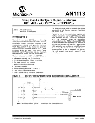
SlideShare a Scribd company logo
AN1113
                 Using C and a Hardware Module to Interface
                  8051 MCUs with I2C™ Serial EEPROMs
                                                                        This application note is part of a series that provide
    Author:   Alexandru Valeanu                                         source code to help the user implement the protocol
              Microchip Technology Inc.                                 with minimal effort.
                                                                        Figure 1 is the hardware schematic depicting the
                                                                        interface between the Microchip 24XXX series of I2C
INTRODUCTION                                                            serial EEPROMs and NXP’s P89LPC952 8051-based
The 24XXX series serial EEPROMs from Microchip                          MCU. The schematic shows the connections
Technology support a bidirectional, 2-wire bus and data                 necessary between the MCU and the serial EEPROM
transmission protocol. The bus is controlled by the                     as tested, as well as the required pull-up resistors on
microcontroller (master), which generates the Serial                    the clock line (SCL) and data line (SDA). Not illustrated
Clock (SCL), controls the bus access and generates                      in this application note are the write-protect feature and
the Start and Stop conditions, while the 24XXX serial                   the cascading of multiple devices; thus, the WP pin and
EEPROM works as slave. The 24XXX serial                                 address pins A0, A1 and A2 are tied to VSS (ground).
                                                                        The test software was written assuming these
EEPROMs are I2C™ compatible and have maximum
                                                                        connections.
clock frequencies ranging from 100 kHz to 1 MHz.
The main features of the 24XXX serial EEPROMs are:
•   2-wire serial interface bus, I2C compatible
•   EEPROM densities from 128 bits to 512 Kbits
•   Bus speed from 100 kHz to 1 MHz
•   Voltage range from 1.7V to 5.5V
•   Low power operation
•   Temperature range from -40°C to +125°C
•   Over 1,000,000 erase/write cycles
•   Up to 8 devices may be connected to same bus

FIGURE 1:             CIRCUIT FOR P89LPC952 MCU AND 24XXX SERIES I2C SERIAL EEPROM
                                                Vcc


                         24XX512


               A0    1             8    Vcc
                                                              4.7 kΩ
               A1    2             7    WP
                                                                                     P1.3 INT0/SDA       7
               A2    3             6    SCL                                             P1.2 T0/SCL      8
                                                                                                             P89LPC952
              Vss    4             5    SDA


        Note: A decoupling capacitor (typically 0.1 µF) should be used to filter noise on VCC.


© 2008 Microchip Technology Inc.                                                                                DS01113B-page 1
AN1113
FIRMWARE DESCRIPTION                                           I2C Functions
                                                               When an MCU accesses an I2C serial EEPROM, it is
Main Function                                                  always the master on the I2C bus and the I2C serial
The purpose of the firmware is to show how to generate         EEPROM is the slave. The MCU controls all operations
specific I2C bus transactions using the bidirectional          on the bus. Each operation is started by the MCU
SDA pin on the microcontroller. The focus is to provide        through a Start condition, followed by a control byte.
the designer with a strong understanding of communi-           The control byte consists of the control code (first 4
cation with the 24XXX series serial EEPROMs, thus              bits), the device address (next 3 bits), and the read/
allowing for more complex programs to be written in the        write (R/ W) bit. The control code is always the same for
future. The firmware was written in C for NXP’s                the serial EEPROM being accessed, while the device
P89LPC952 MCU using the Keil™ µVision3® IDE and                address can range from ‘000’ to ‘111’, allowing up to
was developed on the Keil MCB950 evaluation board.             eight different devices on the same bus. The R/ W bit
                                                               tells the serial EEPROM which operation to perform.
The main code demonstrates two different methods of
accessing the I2C serial EEPROM: byte access and               To access an I2C serial EEPROM at the start, the MCU
page access. The byte method accesses single bytes,            writes the device address and the byte address to the
where every data byte is preceded by three bytes of            I2C serial EEPROM; thus, each access cycle starts
address: device address, MSB address, and LSB                  with a Write condition. For read operations, after the
address. In the page access method, the MCU sends              above sequence, the MCU switches from Transmitter
the address of the first byte, and the I2C serial              mode to Receiver mode and the serial EEPROM from
EEPROM internally increments the address pointer for           Receiver to Transmitter mode through a Restart
the next data byte.                                            condition.

The code was tested using the 24XX512 serial                   BYTE WRITE OPERATION
EEPROM. The EEPROM features 64K x 8 (512 Kbit) of
                                                               Figure 2 depicts the necessary components that
memory and a page write capability of up to 128 bytes
                                                               comprise the byte write operation. Each MCU’s action
of data. Oscilloscope screen shots are shown in this
                                                               is acknowledged (ACK) by the I2C serial EEPROM on
application note. All timings are based on the internal
                                                               the 9th bit of the clock by pulling down the SDA data
RC oscillator of the MCU (7.373 MHz). If a faster clock
                                                               line; consequently, every byte transfer lasts for 9 clock
is used, the code must be modified to generate the
                                                               transitions.
correct delays.
The bus speed in these examples is ~75 kHz.

FIGURE 2:            BYTE WRITE
                              S
            Bus Activity      T Control Byte/                                                              S
                                                     MSB Address       LSB Address
            MCU               A                                                                            T
                              R Device Address          Byte              Byte            Data Byte        O
                              T                                                                            P
            SDA Line          S1 0 1 0AAA 0
                                        2 10                                                               P

            Bus Activity                         A                 A                 A                 A
                                                 C                 C                 C                 C
                                                 K                 K                 K                 K


DS01113B-page 2                                                                          © 2008 Microchip Technology Inc.
AN1113
BYTE READ OPERATION
Figure 3 depicts the necessary components that
comprise the byte read operation. The second Start
condition instructs the I2C serial EEPROM to place
data on the I2C bus.
The SDA line must remain stable while the SCL clock
line is high. Any change of the SDA line while the SCL
line is high is interpreted by the I2C serial EEPROM as
a Start or Stop condition.

FIGURE 3:            BYTE READ
                     S                                                            S
   Bus Activity      T                                                            T                                             S
   MCU               A Control Byte/         MSB Address       LSB Address        A Control Byte/                               T
                     R Device Address           Byte              Byte            R Device Address          Data Byte           O
                     T                                                            T                                             P
   SDA Line          S1 010 AAA0                                                  S 1 0 1 0 A A A1                              P
                               2 1 0                                                        2 1 0
                                        A                  A                  A                      A                      N
   Bus Activity                         C                  C                  C                      C                      A
                                        K                  K                  K                      K                      C
                                                                                                                            K


PAGE WRITE OPERATION
Figure 4 depicts the necessary components that
comprise the page write operation. The only difference
between the page write operation and the byte write
operation (Figure 2) is that the MCU, instead of
sending 1 byte, sends ‘n’ bytes of data, up to the
maximum page size of the I2C serial EEPROM.

FIGURE 4:            PAGE WRITE
                     S
                     T                                                                                                              S
  Bus Activity       A Control Byte/         MSB Address       LSB Address                                                          T
  MCU                R Device Address           Byte              Byte            Data Byte 0             Data Byte 127             O
                     T                                                                                                              P
  SDA Line                     AAA                                                                                                  P
                     S10102 1 00
                                        A                  A                  A                  A                              A
  Bus Activity                          C                  C                  C                  C                              C
                                        K                  K                  K                  K                              K


SEQUENTIAL READ OPERATION
Figure 5 depicts the necessary components that
comprise the sequential read operation. The last read
byte is not acknowledged (NACK) by the MCU. This
terminates the sequential read operation.

FIGURE 5:            SEQUENTIAL READ
                                                                                                                            S
      Bus Activity                                                                                                          T
      MCU            Device Address         Data (n)       Data (n + 1)       Data (n + 2)               Data (n + x)       O
                                                                                                                            P

      SDA Line                                                                                                              P
                                   A                   A                  A                  A                          N
                                   C                   C                  C                  C                          A
      Bus Activity                                                                                                      C
                                   K                   K                  K                  K
                                                                                                                        K


© 2008 Microchip Technology Inc.                                                                               DS01113B-page 3
AN1113
INITIALIZATION                                                                                     START DATA TRANSFER
Initialization consists of initializing the hardware                                               The MCU generates a Start condition on the I2C bus to
peripheral within the MCU. It performs the following                                               initiate data transfer.
actions:                                                                                           Figure 6 shows a typical scope plot from the beginning
• I2EN = 1; //enable I2C part                                                                      of a write operation. Any memory access begins with a
• CRSEL = 0; //select internal baud                                                                Start condition. This is followed by the I2C serial
  generator                                                                                        EEPROM (slave) address (A0h). Because the R/ W bit
• STA = STO = SI = AA = 0; //clear Start,                                                          is set to ‘0’, the next operation of the bus is a write.
  Stop, serial flag, ACK bit
• Sets the bus speed at ~75 kHz: I2SCLL =
  I2SCLH = 25
The bit frequency (fbit) will be:

EQUATION 1:                           BIT RATE

                                            fPCLK
          f         = -------------------------------------------------------------
                                                                                  -
              bit     2 × [ I2SCLH + I2SCLL ]


FIGURE 6:                        I2C START BIT AND SLAVE ADDRESS


                                                                                            S
                                                                             Bus Activity   T
                                                                             MCU            A Control Byte/
                                                                                            R Device Address
                                                                                            T
                                                                             SDA Line       S10 100 000

                                                                             Bus Activity                      A
                                                                                                               C
                                                                                                               K


DS01113B-page 4                                                                                                            © 2008 Microchip Technology Inc.
AN1113
STOP DATA TRANSFER
The MCU generates a Stop condition on the I2C bus to
stop data transfer.
Figure 7 shows a typical scope plot of a byte write
operation followed by a Stop condition. Every operation
on the I2C bus ends with a Stop condition.

FIGURE 7:           BYTE WRITE AND STOP CONDITION


                                                                              S
                                         Bus Activity                         T
                                         MCU                  Data Byte       O
                                                                              P
                                         SDA Line                             P

                                         Bus Activity     A               A
                                                          C               C
                                                          K               K


© 2008 Microchip Technology Inc.                                                  DS01113B-page 5
AN1113
REPEATED START                                                    WRITE I2C SERIAL EEPROM
The Repeated Start condition switches the MCU from                ADDRESS AND READ CONDITION
Transmitter to Receiver mode and the serial EEPROM                Following the Repeated Start condition, the MCU writes
from Receiver to Transmitter. The bit is followed by the          the I2C serial EEPROM address (slave address) with
write of the I2C device address and R/ W bit sequence.            the R/ W bit set correctly.
The sequence is presented in Figure 8.                            For read sequences, the I2C serial EEPROM address
                                                                  is A1h because the R/ W bit is ‘1’, indicating that the
                                                                  MCU waits to read bytes from the I2C serial EEPROM.
                                                                  The sequence is presented in Figure 8.

FIGURE 8:           REPEATED START AND I2C SERIAL EEPROM (SLAVE) ADDRESS


                                                           S
                                                           T
                                           Bus Activity    A
                                                              Control Byte/
                                           MCU             R Device Address
                                                           T
                                           SDA Line        S 1 0 1 0 0 0 0 1
                                                                               A
                                           Bus Activity                        C
                                                                               K


DS01113B-page 6                                                                           © 2008 Microchip Technology Inc.
AN1113
WRITE DEVICE ADDRESS AND
ADDRESS BYTES
After the Start condition, the MCU writes three bytes,
consisting of the device address and the MSB and LSB
addresses. Because the device address is followed by
the write of the two address bytes, the device address
has the R/ W bit set to ‘0’.
The scope plot in Figure 9 depicts the MSB address
byte (00h), the LSB address byte (60h), followed by the
first written byte (through the byte access method) of
the string (43h). Because the byte access method
accesses single bytes, the data byte is followed by a
Stop bit.
The short spikes observed in the scope plot represent
a short period of time during which both the MCU and
the I2C serial EEPROM release the data bus.

FIGURE 9:           WRITE MSB AND LSB ADDRESS BYTES


                                   Bus Activity       MSB Address       LSB Address
                                   MCU                   Byte              Byte

                                   SDA Line

                                   Bus Activity   A                 A                 A
                                                  C                 C                 C
                                                  K                 K                 K


© 2008 Microchip Technology Inc.                                                          DS01113B-page 7
AN1113
WRITE 8 BITS OF DATA                                           READ 8 BITS OF DATA
The write data function is used in both byte write and         The read data function is used in both byte read and
page write operations. The structure of the byte write         sequential read operations. The structure of the byte
operation is shown in Figure 2. The structure of the           read operation is shown in Figure 3. The structure of
page write operation is shown in Figure 4. The only            the sequential read operation is shown in Figure 5.
difference between the two operations is that in the           In the byte read operation, the 8-bit read data is
page write operation the MCU sends ‘n’ bytes of data           situated at the end of the command and is not acknowl-
instead of only one.                                           edged by the MCU through a NACK on the 9th clock
As a rule, the function shifts from a parallel format to the   pulse of the read data byte, which is shown in
serial I2C format. The bus speed is in accordance with         Figure 10.
the initialization routine and is ~75 kHz.                     In the case of a sequential read operation, the last read
The MCU sets the data line on the falling edge of the          byte will be not acknowledged and the other <n-1> read
clock, and the I2C serial EEPROM latches this in on the        bytes will be acknowledged by the MCU.
rising edge of the clock.
In Figure 6 a spike labeled “bus release” can be seen
between the 9th clock pulse and the next clock pulse.
The spike is the sign that both devices – the MCU and
the I2C serial EEPROM – released the open-drain SDA
line in order to be able to continue the communication.

FIGURE 10:           BYTE READ, NACK AND STOP CONDITION


                                                                            S
                                                               Data         T
                                             Bus Activity      Byte         O
                                             MCU                            P

                                             SDA Line                       P
                                                                        N
                                             Bus Activity               A
                                                                        C
                                                                        K


DS01113B-page 8                                                                        © 2008 Microchip Technology Inc.
AN1113
WRITE DATA BYTE                                             WRITE A STRING (PAGE WRITE)
The structure of this byte write operation is shown in      In this application note, the length of the string is
Figure 2. Basically the function consists of a sequence     16 bytes and the physical page size for the 24XX512 is
of function calls. The start data transfer sequence is      128 bytes. The length of the written string must be
described in detail in the section entitled “Start Data     shorter than the physical page size. If the page write
Transfer” and in Figure 6. The stop data transfer           operation overwrites the physical page boundary, the
sequence is described in detail in the section entitled     internal address counter rolls over and overwrites the
“Stop Data Transfer” and in Figure 7. The write MSB         first bytes of the current page.
and LSB address byte sequence is described in the           The structure of the page write operation is shown in
section entitled “Write Device Address and Address          Figure 4.
Bytes” and in Figure 9.
                                                            The sequence must send the address of the first byte
                                                            to be written. The address is automatically incremented
READ DATA BYTE                                              at every byte write by the internal logic of the I2C serial
The read data byte function reads a data byte from the      EEPROM. Each received byte is acknowledged by the
I2C serial EEPROM. The structure of the operation is        EEPROM.
shown in Figure 3.                                          The scope plot in Figure 11 depicts the write of the first
After the first Start condition, the MCU sends the device   three consecutive bytes.
address, the MSB address byte, then the LSB address
byte to the I2C serial EEPROM.
Once the entire memory address has been sent to the
serial EEPROM, a new Start condition is generated to
switch the MCU from Transmitter to Receiver mode
and the serial EEPROM from Receiver to Transmitter
mode. Before the read, the MCU must send a new
device address for a read.
The MCU must generate the necessary NACK or ACK
conditions to terminate or continue the bus operation.


© 2008 Microchip Technology Inc.                                                                    DS01113B-page 9
AN1113
FIGURE 11:         PAGE WRITE (FIRST 3 BYTES)


                           Bus Activity   Data Byte 0       Data Byte 127
                           MCU
                           SDA Line

                           Bus Activity                 A                   A
                                                        C                   C
                                                        K                   K


DS01113B-page 10                                                                © 2008 Microchip Technology Inc.
AN1113
READ A STRING (SEQUENTIAL
READ)
In contrast to the page write operation described in the
previous paragraph, there is no maximum length for a
sequential read. After 64 Kbytes have been read, the
internal address counter rolls over to the beginning of
the array.
To indicate the end of the read, the MCU sends a NACK
before the Stop condition. All other previously read
bytes are acknowledged by the MCU.
The structure of the sequential read operation is shown
in Figure 5. Figure 12 shows a typical scope plot
depicting this operation.

FIGURE 12:          SEQUENTIAL READ (FIRST BYTES)


                                   Bus Activity      Data (n)       Data (n + 1)
                                   MCU
                                   SDA Line
                                   Bus Activity                 A                  A
                                                                C                  C
                                                                K                  K


© 2008 Microchip Technology Inc.                                                       DS01113B-page 11
AN1113
BYTE WRITE VERSUS PAGE WRITE                                The following summarizes the differences between the
                                                            byte write and page write methods.
At first glance, the page write method appears superior
to the byte write method: it’s simpler and faster.          Byte Write
However, a careful analysis shows that the byte write
method has a major advantage over page write owing          • Is slower – It needs a 5 ms write cycle time for
to the roll-over phenomenon (see Note).                       each byte.
                                                            • Is more general – It may write a string of any
  Note:     Page write operations are limited to writing      length.
            bytes within a single physical page,
            regardless of the number of bytes actually      Page Write
            being written. Physical page boundaries
            start at addresses that are integer             • Is faster – It needs only one write cycle time for
            multiples of the page buffer size (or page        the whole page.
            size), and they end at addresses that are       • Care must be taken to observe page boundaries
            integer multiples of [page size-1]. If a          during page writes.
            Page Write command attempts to write
            across a physical page boundary, the            CONCLUSION
            result is that the data wraps around to the
            beginning of the current page (overwriting      This application note offers designers a set of firmware
            data previously stored there) instead of        routines to access I2C serial EEPROMs using a
            being written to the next page as might be      hardware peripheral. The code demonstrates byte and
            expected. It is therefore necessary for the     page operations. All routines were written in C for an
            application software to prevent page write      8051-based MCU.
            operations that would attempt to cross a        The code was developed on the Keil MCB950
            page boundary.                                  evaluation board using the schematic shown in
                                                            Figure 1. It was tested using the NXP P89LPC952
As a consequence of the roll-over phenomenon, appli-        MCU and debugged using the Keil µVision3 IDE.
cations that write long strings to the I2C serial
EEPROM risk overlapping the page boundary in the
middle of a string. In such instances, the firmware
should use byte write to avoid this condition. The disad-
vantage of doing this is the slower speed involved in
writing the entire string: every byte write cycle time is
approximately 5 ms.


DS01113B-page 12                                                                    © 2008 Microchip Technology Inc.
Note the following details of the code protection feature on Microchip devices:
•    Microchip products meet the specification contained in their particular Microchip Data Sheet.

•    Microchip believes that its family of products is one of the most secure families of its kind on the market today, when used in the
     intended manner and under normal conditions.

•    There are dishonest and possibly illegal methods used to breach the code protection feature. All of these methods, to our
     knowledge, require using the Microchip products in a manner outside the operating specifications contained in Microchip’s Data
     Sheets. Most likely, the person doing so is engaged in theft of intellectual property.

•    Microchip is willing to work with the customer who is concerned about the integrity of their code.

•    Neither Microchip nor any other semiconductor manufacturer can guarantee the security of their code. Code protection does not
     mean that we are guaranteeing the product as “unbreakable.”

Code protection is constantly evolving. We at Microchip are committed to continuously improving the code protection features of our
products. Attempts to break Microchip’s code protection feature may be a violation of the Digital Millennium Copyright Act. If such acts
allow unauthorized access to your software or other copyrighted work, you may have a right to sue for relief under that Act.


Information contained in this publication regarding device               Trademarks
applications and the like is provided only for your convenience          The Microchip name and logo, the Microchip logo, Accuron,
and may be superseded by updates. It is your responsibility to
                                                                         dsPIC, KEELOQ, KEELOQ logo, MPLAB, PIC, PICmicro,
ensure that your application meets with your specifications.
                                                                         PICSTART, PRO MATE, rfPIC and SmartShunt are registered
MICROCHIP MAKES NO REPRESENTATIONS OR                                    trademarks of Microchip Technology Incorporated in the
WARRANTIES OF ANY KIND WHETHER EXPRESS OR
                                                                         U.S.A. and other countries.
IMPLIED, WRITTEN OR ORAL, STATUTORY OR
OTHERWISE, RELATED TO THE INFORMATION,                                   FilterLab, Linear Active Thermistor, MXDEV, MXLAB,
INCLUDING BUT NOT LIMITED TO ITS CONDITION,                              SEEVAL, SmartSensor and The Embedded Control Solutions
QUALITY, PERFORMANCE, MERCHANTABILITY OR                                 Company are registered trademarks of Microchip Technology
FITNESS FOR PURPOSE. Microchip disclaims all liability                   Incorporated in the U.S.A.
arising from this information and its use. Use of Microchip              Analog-for-the-Digital Age, Application Maestro, CodeGuard,
devices in life support and/or safety applications is entirely at        dsPICDEM, dsPICDEM.net, dsPICworks, dsSPEAK, ECAN,
the buyer’s risk, and the buyer agrees to defend, indemnify and          ECONOMONITOR, FanSense, In-Circuit Serial
hold harmless Microchip from any and all damages, claims,                Programming, ICSP, ICEPIC, Mindi, MiWi, MPASM, MPLAB
suits, or expenses resulting from such use. No licenses are              Certified logo, MPLIB, MPLINK, mTouch, PICkit, PICDEM,
conveyed, implicitly or otherwise, under any Microchip                   PICDEM.net, PICtail, PIC32 logo, PowerCal, PowerInfo,
intellectual property rights.                                            PowerMate, PowerTool, REAL ICE, rfLAB, Select Mode, Total
                                                                         Endurance, UNI/O, WiperLock and ZENA are trademarks of
                                                                         Microchip Technology Incorporated in the U.S.A. and other
                                                                         countries.
                                                                         SQTP is a service mark of Microchip Technology Incorporated
                                                                         in the U.S.A.
                                                                         All other trademarks mentioned herein are property of their
                                                                         respective companies.
                                                                         © 2008, Microchip Technology Incorporated, Printed in the
                                                                         U.S.A., All Rights Reserved.
                                                                              Printed on recycled paper.


                                                                         Microchip received ISO/TS-16949:2002 certification for its worldwide
                                                                         headquarters, design and wafer fabrication facilities in Chandler and
                                                                         Tempe, Arizona; Gresham, Oregon and design centers in California
                                                                         and India. The Company’s quality system processes and procedures
                                                                         are for its PIC® MCUs and dsPIC® DSCs, KEELOQ® code hopping
                                                                         devices, Serial EEPROMs, microperipherals, nonvolatile memory and
                                                                         analog products. In addition, Microchip’s quality system for the design
                                                                         and manufacture of development systems is ISO 9001:2000 certified.


© 2008 Microchip Technology Inc.                                                                                         DS01113B-page 13
WORLDWIDE SALES AND SERVICE
AMERICAS                        ASIA/PACIFIC                 ASIA/PACIFIC                  EUROPE
Corporate Office                Asia Pacific Office          India - Bangalore             Austria - Wels
2355 West Chandler Blvd.        Suites 3707-14, 37th Floor   Tel: 91-80-4182-8400          Tel: 43-7242-2244-39
Chandler, AZ 85224-6199         Tower 6, The Gateway         Fax: 91-80-4182-8422          Fax: 43-7242-2244-393
Tel: 480-792-7200               Harbour City, Kowloon        India - New Delhi             Denmark - Copenhagen
Fax: 480-792-7277               Hong Kong                                                  Tel: 45-4450-2828
                                                             Tel: 91-11-4160-8631
Technical Support:              Tel: 852-2401-1200                                         Fax: 45-4485-2829
                                                             Fax: 91-11-4160-8632
http://support.microchip.com
                                Fax: 852-2401-3431                                         France - Paris
Web Address:                                                 India - Pune
                                Australia - Sydney           Tel: 91-20-2566-1512          Tel: 33-1-69-53-63-20
www.microchip.com
                                Tel: 61-2-9868-6733          Fax: 91-20-2566-1513          Fax: 33-1-69-30-90-79
Atlanta                         Fax: 61-2-9868-6755
Duluth, GA                                                   Japan - Yokohama              Germany - Munich
                                China - Beijing              Tel: 81-45-471- 6166          Tel: 49-89-627-144-0
Tel: 678-957-9614
                                Tel: 86-10-8528-2100                                       Fax: 49-89-627-144-44
Fax: 678-957-1455                                            Fax: 81-45-471-6122
                                Fax: 86-10-8528-2104                                       Italy - Milan
Boston                                                       Korea - Daegu
                                China - Chengdu                                            Tel: 39-0331-742611
Westborough, MA                                              Tel: 82-53-744-4301
                                Tel: 86-28-8665-5511         Fax: 82-53-744-4302           Fax: 39-0331-466781
Tel: 774-760-0087
                                Fax: 86-28-8665-7889                                       Netherlands - Drunen
Fax: 774-760-0088                                            Korea - Seoul
                                China - Hong Kong SAR        Tel: 82-2-554-7200            Tel: 31-416-690399
Chicago
Itasca, IL                      Tel: 852-2401-1200           Fax: 82-2-558-5932 or         Fax: 31-416-690340
Tel: 630-285-0071               Fax: 852-2401-3431           82-2-558-5934                 Spain - Madrid
Fax: 630-285-0075               China - Nanjing                                            Tel: 34-91-708-08-90
                                                             Malaysia - Kuala Lumpur
                                Tel: 86-25-8473-2460                                       Fax: 34-91-708-08-91
Dallas                                                       Tel: 60-3-6201-9857
Addison, TX                     Fax: 86-25-8473-2470         Fax: 60-3-6201-9859           UK - Wokingham
Tel: 972-818-7423               China - Qingdao                                            Tel: 44-118-921-5869
                                                             Malaysia - Penang
Fax: 972-818-2924               Tel: 86-532-8502-7355                                      Fax: 44-118-921-5820
                                                             Tel: 60-4-227-8870
Detroit                         Fax: 86-532-8502-7205        Fax: 60-4-227-4068
Farmington Hills, MI            China - Shanghai             Philippines - Manila
Tel: 248-538-2250               Tel: 86-21-5407-5533         Tel: 63-2-634-9065
Fax: 248-538-2260               Fax: 86-21-5407-5066         Fax: 63-2-634-9069
Kokomo                          China - Shenyang             Singapore
Kokomo, IN                      Tel: 86-24-2334-2829         Tel: 65-6334-8870
Tel: 765-864-8360               Fax: 86-24-2334-2393         Fax: 65-6334-8850
Fax: 765-864-8387
                                China - Shenzhen             Taiwan - Hsin Chu
Los Angeles                     Tel: 86-755-8203-2660        Tel: 886-3-572-9526
Mission Viejo, CA               Fax: 86-755-8203-1760        Fax: 886-3-572-6459
Tel: 949-462-9523
                                China - Wuhan                Taiwan - Kaohsiung
Fax: 949-462-9608
                                Tel: 86-27-5980-5300         Tel: 886-7-536-4818
Santa Clara                     Fax: 86-27-5980-5118         Fax: 886-7-536-4803
Santa Clara, CA
                                China - Xiamen               Taiwan - Taipei
Tel: 408-961-6444
                                Tel: 86-592-2388138          Tel: 886-2-2500-6610
Fax: 408-961-6445
                                Fax: 86-592-2388130          Fax: 886-2-2508-0102
Toronto
                                China - Xian                 Thailand - Bangkok
Mississauga, Ontario,
                                Tel: 86-29-8833-7252         Tel: 66-2-694-1351
Canada
Tel: 905-673-0699               Fax: 86-29-8833-7256         Fax: 66-2-694-1350
Fax: 905-673-6509               China - Zhuhai
                                Tel: 86-756-3210040
                                Fax: 86-756-3210049


                                                                                                            01/02/08


DS01113B-page 14                                                                       © 2008 Microchip Technology Inc.

More Related Content

What's hot

ARM COMPLETE DETAIL PART 4
ARM COMPLETE DETAIL PART 4ARM COMPLETE DETAIL PART 4
ARM COMPLETE DETAIL PART 4
NOWAY
 
8051f044
8051f0448051f044
Rfid interface with lpc2148
Rfid interface with lpc2148 Rfid interface with lpc2148
Rfid interface with lpc2148
Ritesh Kumar
 
EMBEDDED PASSWORD BASED ACESS CONTROL SYSTEM USING I2C PROTOCOL
EMBEDDED PASSWORD BASED ACESS CONTROL  SYSTEM USING I2C PROTOCOLEMBEDDED PASSWORD BASED ACESS CONTROL  SYSTEM USING I2C PROTOCOL
EMBEDDED PASSWORD BASED ACESS CONTROL SYSTEM USING I2C PROTOCOL
Gaurav Singh
 
Technical Proposal - Public Address
Technical Proposal - Public AddressTechnical Proposal - Public Address
Technical Proposal - Public Address
wolfthrone
 
Showing sound signals on VGA with using PMOD MIC
Showing sound signals on VGA with using PMOD MICShowing sound signals on VGA with using PMOD MIC
Showing sound signals on VGA with using PMOD MICilker Şin
 
AUTOMATIC GRID ON SENSING BAD VOLTAGE OR FREQUENCY
AUTOMATIC GRID ON SENSING BAD VOLTAGE OR FREQUENCYAUTOMATIC GRID ON SENSING BAD VOLTAGE OR FREQUENCY
AUTOMATIC GRID ON SENSING BAD VOLTAGE OR FREQUENCY
Gaurav Singh
 
Digital stop watch
Digital stop watchDigital stop watch
Digital stop watch
Sai Malleswar
 
Navigation of Robot Vehicle using RF with Landmine Detection
Navigation of Robot Vehicle using RF with Landmine DetectionNavigation of Robot Vehicle using RF with Landmine Detection
Navigation of Robot Vehicle using RF with Landmine DetectionVeena Rani
 
Pdc 2 mark
Pdc   2 markPdc   2 mark
Pdc 2 mark
balaji1986
 
water level controller using 8051 microcontroller
water level controller using 8051 microcontrollerwater level controller using 8051 microcontroller
water level controller using 8051 microcontroller
Prachi Pandey
 
Arm7 document
Arm7  documentArm7  document
Arm7 document
N Harisha
 
Technical Proposal - IP Telephony
Technical Proposal - IP Telephony Technical Proposal - IP Telephony
Technical Proposal - IP Telephony
wolfthrone
 
User.manual.lpc11xx.lpc11cxx
User.manual.lpc11xx.lpc11cxxUser.manual.lpc11xx.lpc11cxx
User.manual.lpc11xx.lpc11cxx
yateeshk
 
Technical Proposal - Structured Cabling
Technical Proposal - Structured CablingTechnical Proposal - Structured Cabling
Technical Proposal - Structured Cabling
wolfthrone
 
GarrettCom 10KT Substation Switch Now Available
GarrettCom 10KT Substation Switch Now AvailableGarrettCom 10KT Substation Switch Now Available
GarrettCom 10KT Substation Switch Now Available
mikemount66
 
RTC Interfacing and Programming
RTC Interfacing and ProgrammingRTC Interfacing and Programming
RTC Interfacing and Programming
Devashish Raval
 

What's hot (20)

ARM COMPLETE DETAIL PART 4
ARM COMPLETE DETAIL PART 4ARM COMPLETE DETAIL PART 4
ARM COMPLETE DETAIL PART 4
 
8051f044
8051f0448051f044
8051f044
 
Rfid interface with lpc2148
Rfid interface with lpc2148 Rfid interface with lpc2148
Rfid interface with lpc2148
 
EMBEDDED PASSWORD BASED ACESS CONTROL SYSTEM USING I2C PROTOCOL
EMBEDDED PASSWORD BASED ACESS CONTROL  SYSTEM USING I2C PROTOCOLEMBEDDED PASSWORD BASED ACESS CONTROL  SYSTEM USING I2C PROTOCOL
EMBEDDED PASSWORD BASED ACESS CONTROL SYSTEM USING I2C PROTOCOL
 
project 3 full report
project 3 full reportproject 3 full report
project 3 full report
 
Technical Proposal - Public Address
Technical Proposal - Public AddressTechnical Proposal - Public Address
Technical Proposal - Public Address
 
Showing sound signals on VGA with using PMOD MIC
Showing sound signals on VGA with using PMOD MICShowing sound signals on VGA with using PMOD MIC
Showing sound signals on VGA with using PMOD MIC
 
Ia ec700-c-r1
Ia ec700-c-r1Ia ec700-c-r1
Ia ec700-c-r1
 
AUTOMATIC GRID ON SENSING BAD VOLTAGE OR FREQUENCY
AUTOMATIC GRID ON SENSING BAD VOLTAGE OR FREQUENCYAUTOMATIC GRID ON SENSING BAD VOLTAGE OR FREQUENCY
AUTOMATIC GRID ON SENSING BAD VOLTAGE OR FREQUENCY
 
Digital stop watch
Digital stop watchDigital stop watch
Digital stop watch
 
Navigation of Robot Vehicle using RF with Landmine Detection
Navigation of Robot Vehicle using RF with Landmine DetectionNavigation of Robot Vehicle using RF with Landmine Detection
Navigation of Robot Vehicle using RF with Landmine Detection
 
Pdc 2 mark
Pdc   2 markPdc   2 mark
Pdc 2 mark
 
water level controller using 8051 microcontroller
water level controller using 8051 microcontrollerwater level controller using 8051 microcontroller
water level controller using 8051 microcontroller
 
Arm7 document
Arm7  documentArm7  document
Arm7 document
 
Technical Proposal - IP Telephony
Technical Proposal - IP Telephony Technical Proposal - IP Telephony
Technical Proposal - IP Telephony
 
User.manual.lpc11xx.lpc11cxx
User.manual.lpc11xx.lpc11cxxUser.manual.lpc11xx.lpc11cxx
User.manual.lpc11xx.lpc11cxx
 
Technical Proposal - Structured Cabling
Technical Proposal - Structured CablingTechnical Proposal - Structured Cabling
Technical Proposal - Structured Cabling
 
GarrettCom 10KT Substation Switch Now Available
GarrettCom 10KT Substation Switch Now AvailableGarrettCom 10KT Substation Switch Now Available
GarrettCom 10KT Substation Switch Now Available
 
Chapter5 dek3133
Chapter5 dek3133Chapter5 dek3133
Chapter5 dek3133
 
RTC Interfacing and Programming
RTC Interfacing and ProgrammingRTC Interfacing and Programming
RTC Interfacing and Programming
 

Viewers also liked

Verkko ja nuorisotyön toimintaympäristö, Päivi Timonen, Humak (2013 syksy)
Verkko ja nuorisotyön toimintaympäristö, Päivi Timonen, Humak (2013 syksy)Verkko ja nuorisotyön toimintaympäristö, Päivi Timonen, Humak (2013 syksy)
Verkko ja nuorisotyön toimintaympäristö, Päivi Timonen, Humak (2013 syksy)
PTimonen, Humak, Humanistinen ammattikorkeakoulu
 
Johda ja hyödynnä sosiaalista mediaa – työkalupakki kunnan nuorisotyön johtam...
Johda ja hyödynnä sosiaalista mediaa – työkalupakki kunnan nuorisotyön johtam...Johda ja hyödynnä sosiaalista mediaa – työkalupakki kunnan nuorisotyön johtam...
Johda ja hyödynnä sosiaalista mediaa – työkalupakki kunnan nuorisotyön johtam...
PTimonen, Humak, Humanistinen ammattikorkeakoulu
 
Софіт №6(10)
Софіт №6(10)Софіт №6(10)
Софіт №6(10)
Sofit Lux
 
Софіт №8(12)
Софіт №8(12)Софіт №8(12)
Софіт №8(12)
Sofit Lux
 
Asce Presentation
Asce PresentationAsce Presentation
Asce Presentationalexsndiego
 
OpenStreetMap integration into Wikimedia projects
OpenStreetMap integration into Wikimedia projectsOpenStreetMap integration into Wikimedia projects
OpenStreetMap integration into Wikimedia projects
avarab
 
Share The Music - Introduction
Share The Music - IntroductionShare The Music - Introduction
Share The Music - Introduction
ShareTheMusic
 
Alunos da 2ª fase do 1º ciclo
Alunos da 2ª fase do 1º cicloAlunos da 2ª fase do 1º ciclo
Alunos da 2ª fase do 1º cicloguest633d1e
 
J W T Anxiety Index Quarterly Summer2009(1)
J W T  Anxiety Index Quarterly  Summer2009(1)J W T  Anxiety Index Quarterly  Summer2009(1)
J W T Anxiety Index Quarterly Summer2009(1)APG México
 
.htaccess Cheatsheet
.htaccess Cheatsheet.htaccess Cheatsheet
.htaccess Cheatsheet
Shankar Soma
 
Blu as presentation
Blu as presentationBlu as presentation
Blu as presentationOnizukar
 
Agha/ Showcase
Agha/ Showcase Agha/ Showcase
Agha/ Showcase
AghaInteriors
 
E source energy managers conf 4 24-13-final
E source energy managers conf 4 24-13-finalE source energy managers conf 4 24-13-final
E source energy managers conf 4 24-13-finaljosh whitney
 
Verkko ja nuorisokulttuurit, nuorten mediakulttuurit -lyhyt oppimäärä :)
Verkko ja nuorisokulttuurit, nuorten mediakulttuurit -lyhyt oppimäärä :)Verkko ja nuorisokulttuurit, nuorten mediakulttuurit -lyhyt oppimäärä :)
Verkko ja nuorisokulttuurit, nuorten mediakulttuurit -lyhyt oppimäärä :)
PTimonen, Humak, Humanistinen ammattikorkeakoulu
 
Каталог GBE
Каталог GBEКаталог GBE
Каталог GBE
Sofit Lux
 
Condiciones del mercado de la carne de ovino en los municipios de la Provinci...
Condiciones del mercado de la carne de ovino en los municipios de la Provinci...Condiciones del mercado de la carne de ovino en los municipios de la Provinci...
Condiciones del mercado de la carne de ovino en los municipios de la Provinci...
79575641
 
Mikkeli210312 sosiaalinenmediatyöpaja
Mikkeli210312 sosiaalinenmediatyöpajaMikkeli210312 sosiaalinenmediatyöpaja
Mikkeli210312 sosiaalinenmediatyöpaja
PTimonen, Humak, Humanistinen ammattikorkeakoulu
 

Viewers also liked (20)

Verkko ja nuorisotyön toimintaympäristö, Päivi Timonen, Humak (2013 syksy)
Verkko ja nuorisotyön toimintaympäristö, Päivi Timonen, Humak (2013 syksy)Verkko ja nuorisotyön toimintaympäristö, Päivi Timonen, Humak (2013 syksy)
Verkko ja nuorisotyön toimintaympäristö, Päivi Timonen, Humak (2013 syksy)
 
Johda ja hyödynnä sosiaalista mediaa – työkalupakki kunnan nuorisotyön johtam...
Johda ja hyödynnä sosiaalista mediaa – työkalupakki kunnan nuorisotyön johtam...Johda ja hyödynnä sosiaalista mediaa – työkalupakki kunnan nuorisotyön johtam...
Johda ja hyödynnä sosiaalista mediaa – työkalupakki kunnan nuorisotyön johtam...
 
Софіт №6(10)
Софіт №6(10)Софіт №6(10)
Софіт №6(10)
 
Софіт №8(12)
Софіт №8(12)Софіт №8(12)
Софіт №8(12)
 
Asce Presentation
Asce PresentationAsce Presentation
Asce Presentation
 
OpenStreetMap integration into Wikimedia projects
OpenStreetMap integration into Wikimedia projectsOpenStreetMap integration into Wikimedia projects
OpenStreetMap integration into Wikimedia projects
 
PresentacióN Makuna
PresentacióN MakunaPresentacióN Makuna
PresentacióN Makuna
 
Share The Music - Introduction
Share The Music - IntroductionShare The Music - Introduction
Share The Music - Introduction
 
Alunos da 2ª fase do 1º ciclo
Alunos da 2ª fase do 1º cicloAlunos da 2ª fase do 1º ciclo
Alunos da 2ª fase do 1º ciclo
 
J W T Anxiety Index Quarterly Summer2009(1)
J W T  Anxiety Index Quarterly  Summer2009(1)J W T  Anxiety Index Quarterly  Summer2009(1)
J W T Anxiety Index Quarterly Summer2009(1)
 
Out
OutOut
Out
 
.htaccess Cheatsheet
.htaccess Cheatsheet.htaccess Cheatsheet
.htaccess Cheatsheet
 
Blu as presentation
Blu as presentationBlu as presentation
Blu as presentation
 
Agha/ Showcase
Agha/ Showcase Agha/ Showcase
Agha/ Showcase
 
E source energy managers conf 4 24-13-final
E source energy managers conf 4 24-13-finalE source energy managers conf 4 24-13-final
E source energy managers conf 4 24-13-final
 
Verkko ja nuorisokulttuurit, nuorten mediakulttuurit -lyhyt oppimäärä :)
Verkko ja nuorisokulttuurit, nuorten mediakulttuurit -lyhyt oppimäärä :)Verkko ja nuorisokulttuurit, nuorten mediakulttuurit -lyhyt oppimäärä :)
Verkko ja nuorisokulttuurit, nuorten mediakulttuurit -lyhyt oppimäärä :)
 
Каталог GBE
Каталог GBEКаталог GBE
Каталог GBE
 
Condiciones del mercado de la carne de ovino en los municipios de la Provinci...
Condiciones del mercado de la carne de ovino en los municipios de la Provinci...Condiciones del mercado de la carne de ovino en los municipios de la Provinci...
Condiciones del mercado de la carne de ovino en los municipios de la Provinci...
 
DeLux 2011
DeLux 2011DeLux 2011
DeLux 2011
 
Mikkeli210312 sosiaalinenmediatyöpaja
Mikkeli210312 sosiaalinenmediatyöpajaMikkeli210312 sosiaalinenmediatyöpaja
Mikkeli210312 sosiaalinenmediatyöpaja
 

Similar to 01113 b

underground cable fault location using aruino,gsm&gps
underground cable fault location using aruino,gsm&gps underground cable fault location using aruino,gsm&gps
underground cable fault location using aruino,gsm&gps
Mohd Sohail
 
ELECTRICAL ENGINEERING PROJECT
ELECTRICAL ENGINEERING PROJECTELECTRICAL ENGINEERING PROJECT
ELECTRICAL ENGINEERING PROJECT
vasav2204
 
electrical engineering project
electrical engineering projectelectrical engineering project
electrical engineering project
vasav2204
 
Precise kilometer calculation by underground cable fault detector
Precise kilometer calculation by underground cable fault detectorPrecise kilometer calculation by underground cable fault detector
Precise kilometer calculation by underground cable fault detector
vivekmv716
 
Overview of Microcontroller and ATMega32 microcontroller
Overview of Microcontroller and ATMega32 microcontrollerOverview of Microcontroller and ATMega32 microcontroller
Overview of Microcontroller and ATMega32 microcontroller
Rup Chowdhury
 
IEEE Paper A SystemC AMS Model of an I2C Bus Controller
IEEE Paper A SystemC AMS Model  of an I2C Bus ControllerIEEE Paper A SystemC AMS Model  of an I2C Bus Controller
IEEE Paper A SystemC AMS Model of an I2C Bus Controller
Dweapons Art
 
under grund fault ppt (1).pptx
under grund fault ppt (1).pptxunder grund fault ppt (1).pptx
under grund fault ppt (1).pptx
PoojaG86
 
Assembler4
Assembler4Assembler4
Assembler4
Omar Sanchez
 
Industrial training report of embedded system and robotics
Industrial training report of embedded system and roboticsIndustrial training report of embedded system and robotics
Industrial training report of embedded system and robotics
Pallavi Bharti
 
digital clock atmega16
digital clock atmega16digital clock atmega16
digital clock atmega16
Arcanjo Salazaku
 
Metal Detector Robotic Vehicle
Metal Detector Robotic VehicleMetal Detector Robotic Vehicle
Metal Detector Robotic Vehicle
Edgefxkits & Solutions
 
Coin based mobile charger project report
Coin based mobile charger project reportCoin based mobile charger project report
Coin based mobile charger project report
kaushal chaubey
 
Contactless digital tachometer using microcontroller
Contactless digital tachometer using microcontroller Contactless digital tachometer using microcontroller
Contactless digital tachometer using microcontroller
IJECEIAES
 
Upfc ppt
Upfc pptUpfc ppt
Upfc ppt
sagar shinde
 
Mini project
Mini projectMini project
Mini project
pra16shant
 
Mobile robotic platform to gathering real time sensory data in wireless perso...
Mobile robotic platform to gathering real time sensory data in wireless perso...Mobile robotic platform to gathering real time sensory data in wireless perso...
Mobile robotic platform to gathering real time sensory data in wireless perso...
Alexander Decker
 
Steper Motor Control Through Wireless
Steper Motor Control Through WirelessSteper Motor Control Through Wireless
Steper Motor Control Through Wireless
Pawan Bahuguna
 

Similar to 01113 b (20)

Badal sharma
Badal sharmaBadal sharma
Badal sharma
 
underground cable fault location using aruino,gsm&gps
underground cable fault location using aruino,gsm&gps underground cable fault location using aruino,gsm&gps
underground cable fault location using aruino,gsm&gps
 
ELECTRICAL ENGINEERING PROJECT
ELECTRICAL ENGINEERING PROJECTELECTRICAL ENGINEERING PROJECT
ELECTRICAL ENGINEERING PROJECT
 
electrical engineering project
electrical engineering projectelectrical engineering project
electrical engineering project
 
Precise kilometer calculation by underground cable fault detector
Precise kilometer calculation by underground cable fault detectorPrecise kilometer calculation by underground cable fault detector
Precise kilometer calculation by underground cable fault detector
 
Overview of Microcontroller and ATMega32 microcontroller
Overview of Microcontroller and ATMega32 microcontrollerOverview of Microcontroller and ATMega32 microcontroller
Overview of Microcontroller and ATMega32 microcontroller
 
IEEE Paper A SystemC AMS Model of an I2C Bus Controller
IEEE Paper A SystemC AMS Model  of an I2C Bus ControllerIEEE Paper A SystemC AMS Model  of an I2C Bus Controller
IEEE Paper A SystemC AMS Model of an I2C Bus Controller
 
under grund fault ppt (1).pptx
under grund fault ppt (1).pptxunder grund fault ppt (1).pptx
under grund fault ppt (1).pptx
 
An hemmanur
An hemmanurAn hemmanur
An hemmanur
 
Assembler4
Assembler4Assembler4
Assembler4
 
Industrial training report of embedded system and robotics
Industrial training report of embedded system and roboticsIndustrial training report of embedded system and robotics
Industrial training report of embedded system and robotics
 
digital clock atmega16
digital clock atmega16digital clock atmega16
digital clock atmega16
 
Metal Detector Robotic Vehicle
Metal Detector Robotic VehicleMetal Detector Robotic Vehicle
Metal Detector Robotic Vehicle
 
Coin based mobile charger project report
Coin based mobile charger project reportCoin based mobile charger project report
Coin based mobile charger project report
 
Contactless digital tachometer using microcontroller
Contactless digital tachometer using microcontroller Contactless digital tachometer using microcontroller
Contactless digital tachometer using microcontroller
 
Upfc ppt
Upfc pptUpfc ppt
Upfc ppt
 
Mini project
Mini projectMini project
Mini project
 
Mobile robotic platform to gathering real time sensory data in wireless perso...
Mobile robotic platform to gathering real time sensory data in wireless perso...Mobile robotic platform to gathering real time sensory data in wireless perso...
Mobile robotic platform to gathering real time sensory data in wireless perso...
 
Steper Motor Control Through Wireless
Steper Motor Control Through WirelessSteper Motor Control Through Wireless
Steper Motor Control Through Wireless
 
mini project
mini projectmini project
mini project
 

Recently uploaded

How libraries can support authors with open access requirements for UKRI fund...
How libraries can support authors with open access requirements for UKRI fund...How libraries can support authors with open access requirements for UKRI fund...
How libraries can support authors with open access requirements for UKRI fund...
Jisc
 
The approach at University of Liverpool.pptx
The approach at University of Liverpool.pptxThe approach at University of Liverpool.pptx
The approach at University of Liverpool.pptx
Jisc
 
Polish students' mobility in the Czech Republic
Polish students' mobility in the Czech RepublicPolish students' mobility in the Czech Republic
Polish students' mobility in the Czech Republic
Anna Sz.
 
A Strategic Approach: GenAI in Education
A Strategic Approach: GenAI in EducationA Strategic Approach: GenAI in Education
A Strategic Approach: GenAI in Education
Peter Windle
 
BÀI TẬP BỔ TRỢ TIẾNG ANH GLOBAL SUCCESS LỚP 3 - CẢ NĂM (CÓ FILE NGHE VÀ ĐÁP Á...
BÀI TẬP BỔ TRỢ TIẾNG ANH GLOBAL SUCCESS LỚP 3 - CẢ NĂM (CÓ FILE NGHE VÀ ĐÁP Á...BÀI TẬP BỔ TRỢ TIẾNG ANH GLOBAL SUCCESS LỚP 3 - CẢ NĂM (CÓ FILE NGHE VÀ ĐÁP Á...
BÀI TẬP BỔ TRỢ TIẾNG ANH GLOBAL SUCCESS LỚP 3 - CẢ NĂM (CÓ FILE NGHE VÀ ĐÁP Á...
Nguyen Thanh Tu Collection
 
Welcome to TechSoup New Member Orientation and Q&A (May 2024).pdf
Welcome to TechSoup   New Member Orientation and Q&A (May 2024).pdfWelcome to TechSoup   New Member Orientation and Q&A (May 2024).pdf
Welcome to TechSoup New Member Orientation and Q&A (May 2024).pdf
TechSoup
 
Sha'Carri Richardson Presentation 202345
Sha'Carri Richardson Presentation 202345Sha'Carri Richardson Presentation 202345
Sha'Carri Richardson Presentation 202345
beazzy04
 
Supporting (UKRI) OA monographs at Salford.pptx
Supporting (UKRI) OA monographs at Salford.pptxSupporting (UKRI) OA monographs at Salford.pptx
Supporting (UKRI) OA monographs at Salford.pptx
Jisc
 
Unit 2- Research Aptitude (UGC NET Paper I).pdf
Unit 2- Research Aptitude (UGC NET Paper I).pdfUnit 2- Research Aptitude (UGC NET Paper I).pdf
Unit 2- Research Aptitude (UGC NET Paper I).pdf
Thiyagu K
 
The basics of sentences session 5pptx.pptx
The basics of sentences session 5pptx.pptxThe basics of sentences session 5pptx.pptx
The basics of sentences session 5pptx.pptx
heathfieldcps1
 
The French Revolution Class 9 Study Material pdf free download
The French Revolution Class 9 Study Material pdf free downloadThe French Revolution Class 9 Study Material pdf free download
The French Revolution Class 9 Study Material pdf free download
Vivekanand Anglo Vedic Academy
 
Francesca Gottschalk - How can education support child empowerment.pptx
Francesca Gottschalk - How can education support child empowerment.pptxFrancesca Gottschalk - How can education support child empowerment.pptx
Francesca Gottschalk - How can education support child empowerment.pptx
EduSkills OECD
 
aaaaaaaaaaaaaaaaaaaaaaaaaaaaaaaaaaaaaaaaa
aaaaaaaaaaaaaaaaaaaaaaaaaaaaaaaaaaaaaaaaaaaaaaaaaaaaaaaaaaaaaaaaaaaaaaaaaaaaaaaaaa
aaaaaaaaaaaaaaaaaaaaaaaaaaaaaaaaaaaaaaaaa
siemaillard
 
The Roman Empire A Historical Colossus.pdf
The Roman Empire A Historical Colossus.pdfThe Roman Empire A Historical Colossus.pdf
The Roman Empire A Historical Colossus.pdf
kaushalkr1407
 
The geography of Taylor Swift - some ideas
The geography of Taylor Swift - some ideasThe geography of Taylor Swift - some ideas
The geography of Taylor Swift - some ideas
GeoBlogs
 
Instructions for Submissions thorugh G- Classroom.pptx
Instructions for Submissions thorugh G- Classroom.pptxInstructions for Submissions thorugh G- Classroom.pptx
Instructions for Submissions thorugh G- Classroom.pptx
Jheel Barad
 
Operation Blue Star - Saka Neela Tara
Operation Blue Star   -  Saka Neela TaraOperation Blue Star   -  Saka Neela Tara
Operation Blue Star - Saka Neela Tara
Balvir Singh
 
Unit 8 - Information and Communication Technology (Paper I).pdf
Unit 8 - Information and Communication Technology (Paper I).pdfUnit 8 - Information and Communication Technology (Paper I).pdf
Unit 8 - Information and Communication Technology (Paper I).pdf
Thiyagu K
 
Digital Tools and AI for Teaching Learning and Research
Digital Tools and AI for Teaching Learning and ResearchDigital Tools and AI for Teaching Learning and Research
Digital Tools and AI for Teaching Learning and Research
Vikramjit Singh
 
Synthetic Fiber Construction in lab .pptx
Synthetic Fiber Construction in lab .pptxSynthetic Fiber Construction in lab .pptx
Synthetic Fiber Construction in lab .pptx
Pavel ( NSTU)
 

Recently uploaded (20)

How libraries can support authors with open access requirements for UKRI fund...
How libraries can support authors with open access requirements for UKRI fund...How libraries can support authors with open access requirements for UKRI fund...
How libraries can support authors with open access requirements for UKRI fund...
 
The approach at University of Liverpool.pptx
The approach at University of Liverpool.pptxThe approach at University of Liverpool.pptx
The approach at University of Liverpool.pptx
 
Polish students' mobility in the Czech Republic
Polish students' mobility in the Czech RepublicPolish students' mobility in the Czech Republic
Polish students' mobility in the Czech Republic
 
A Strategic Approach: GenAI in Education
A Strategic Approach: GenAI in EducationA Strategic Approach: GenAI in Education
A Strategic Approach: GenAI in Education
 
BÀI TẬP BỔ TRỢ TIẾNG ANH GLOBAL SUCCESS LỚP 3 - CẢ NĂM (CÓ FILE NGHE VÀ ĐÁP Á...
BÀI TẬP BỔ TRỢ TIẾNG ANH GLOBAL SUCCESS LỚP 3 - CẢ NĂM (CÓ FILE NGHE VÀ ĐÁP Á...BÀI TẬP BỔ TRỢ TIẾNG ANH GLOBAL SUCCESS LỚP 3 - CẢ NĂM (CÓ FILE NGHE VÀ ĐÁP Á...
BÀI TẬP BỔ TRỢ TIẾNG ANH GLOBAL SUCCESS LỚP 3 - CẢ NĂM (CÓ FILE NGHE VÀ ĐÁP Á...
 
Welcome to TechSoup New Member Orientation and Q&A (May 2024).pdf
Welcome to TechSoup   New Member Orientation and Q&A (May 2024).pdfWelcome to TechSoup   New Member Orientation and Q&A (May 2024).pdf
Welcome to TechSoup New Member Orientation and Q&A (May 2024).pdf
 
Sha'Carri Richardson Presentation 202345
Sha'Carri Richardson Presentation 202345Sha'Carri Richardson Presentation 202345
Sha'Carri Richardson Presentation 202345
 
Supporting (UKRI) OA monographs at Salford.pptx
Supporting (UKRI) OA monographs at Salford.pptxSupporting (UKRI) OA monographs at Salford.pptx
Supporting (UKRI) OA monographs at Salford.pptx
 
Unit 2- Research Aptitude (UGC NET Paper I).pdf
Unit 2- Research Aptitude (UGC NET Paper I).pdfUnit 2- Research Aptitude (UGC NET Paper I).pdf
Unit 2- Research Aptitude (UGC NET Paper I).pdf
 
The basics of sentences session 5pptx.pptx
The basics of sentences session 5pptx.pptxThe basics of sentences session 5pptx.pptx
The basics of sentences session 5pptx.pptx
 
The French Revolution Class 9 Study Material pdf free download
The French Revolution Class 9 Study Material pdf free downloadThe French Revolution Class 9 Study Material pdf free download
The French Revolution Class 9 Study Material pdf free download
 
Francesca Gottschalk - How can education support child empowerment.pptx
Francesca Gottschalk - How can education support child empowerment.pptxFrancesca Gottschalk - How can education support child empowerment.pptx
Francesca Gottschalk - How can education support child empowerment.pptx
 
aaaaaaaaaaaaaaaaaaaaaaaaaaaaaaaaaaaaaaaaa
aaaaaaaaaaaaaaaaaaaaaaaaaaaaaaaaaaaaaaaaaaaaaaaaaaaaaaaaaaaaaaaaaaaaaaaaaaaaaaaaaa
aaaaaaaaaaaaaaaaaaaaaaaaaaaaaaaaaaaaaaaaa
 
The Roman Empire A Historical Colossus.pdf
The Roman Empire A Historical Colossus.pdfThe Roman Empire A Historical Colossus.pdf
The Roman Empire A Historical Colossus.pdf
 
The geography of Taylor Swift - some ideas
The geography of Taylor Swift - some ideasThe geography of Taylor Swift - some ideas
The geography of Taylor Swift - some ideas
 
Instructions for Submissions thorugh G- Classroom.pptx
Instructions for Submissions thorugh G- Classroom.pptxInstructions for Submissions thorugh G- Classroom.pptx
Instructions for Submissions thorugh G- Classroom.pptx
 
Operation Blue Star - Saka Neela Tara
Operation Blue Star   -  Saka Neela TaraOperation Blue Star   -  Saka Neela Tara
Operation Blue Star - Saka Neela Tara
 
Unit 8 - Information and Communication Technology (Paper I).pdf
Unit 8 - Information and Communication Technology (Paper I).pdfUnit 8 - Information and Communication Technology (Paper I).pdf
Unit 8 - Information and Communication Technology (Paper I).pdf
 
Digital Tools and AI for Teaching Learning and Research
Digital Tools and AI for Teaching Learning and ResearchDigital Tools and AI for Teaching Learning and Research
Digital Tools and AI for Teaching Learning and Research
 
Synthetic Fiber Construction in lab .pptx
Synthetic Fiber Construction in lab .pptxSynthetic Fiber Construction in lab .pptx
Synthetic Fiber Construction in lab .pptx
 

01113 b

  • 1. AN1113 Using C and a Hardware Module to Interface 8051 MCUs with I2C™ Serial EEPROMs This application note is part of a series that provide Author: Alexandru Valeanu source code to help the user implement the protocol Microchip Technology Inc. with minimal effort. Figure 1 is the hardware schematic depicting the interface between the Microchip 24XXX series of I2C INTRODUCTION serial EEPROMs and NXP’s P89LPC952 8051-based The 24XXX series serial EEPROMs from Microchip MCU. The schematic shows the connections Technology support a bidirectional, 2-wire bus and data necessary between the MCU and the serial EEPROM transmission protocol. The bus is controlled by the as tested, as well as the required pull-up resistors on microcontroller (master), which generates the Serial the clock line (SCL) and data line (SDA). Not illustrated Clock (SCL), controls the bus access and generates in this application note are the write-protect feature and the Start and Stop conditions, while the 24XXX serial the cascading of multiple devices; thus, the WP pin and EEPROM works as slave. The 24XXX serial address pins A0, A1 and A2 are tied to VSS (ground). The test software was written assuming these EEPROMs are I2C™ compatible and have maximum connections. clock frequencies ranging from 100 kHz to 1 MHz. The main features of the 24XXX serial EEPROMs are: • 2-wire serial interface bus, I2C compatible • EEPROM densities from 128 bits to 512 Kbits • Bus speed from 100 kHz to 1 MHz • Voltage range from 1.7V to 5.5V • Low power operation • Temperature range from -40°C to +125°C • Over 1,000,000 erase/write cycles • Up to 8 devices may be connected to same bus FIGURE 1: CIRCUIT FOR P89LPC952 MCU AND 24XXX SERIES I2C SERIAL EEPROM Vcc 24XX512 A0 1 8 Vcc 4.7 kΩ A1 2 7 WP P1.3 INT0/SDA 7 A2 3 6 SCL P1.2 T0/SCL 8 P89LPC952 Vss 4 5 SDA Note: A decoupling capacitor (typically 0.1 µF) should be used to filter noise on VCC. © 2008 Microchip Technology Inc. DS01113B-page 1
  • 2. AN1113 FIRMWARE DESCRIPTION I2C Functions When an MCU accesses an I2C serial EEPROM, it is Main Function always the master on the I2C bus and the I2C serial The purpose of the firmware is to show how to generate EEPROM is the slave. The MCU controls all operations specific I2C bus transactions using the bidirectional on the bus. Each operation is started by the MCU SDA pin on the microcontroller. The focus is to provide through a Start condition, followed by a control byte. the designer with a strong understanding of communi- The control byte consists of the control code (first 4 cation with the 24XXX series serial EEPROMs, thus bits), the device address (next 3 bits), and the read/ allowing for more complex programs to be written in the write (R/ W) bit. The control code is always the same for future. The firmware was written in C for NXP’s the serial EEPROM being accessed, while the device P89LPC952 MCU using the Keil™ µVision3® IDE and address can range from ‘000’ to ‘111’, allowing up to was developed on the Keil MCB950 evaluation board. eight different devices on the same bus. The R/ W bit tells the serial EEPROM which operation to perform. The main code demonstrates two different methods of accessing the I2C serial EEPROM: byte access and To access an I2C serial EEPROM at the start, the MCU page access. The byte method accesses single bytes, writes the device address and the byte address to the where every data byte is preceded by three bytes of I2C serial EEPROM; thus, each access cycle starts address: device address, MSB address, and LSB with a Write condition. For read operations, after the address. In the page access method, the MCU sends above sequence, the MCU switches from Transmitter the address of the first byte, and the I2C serial mode to Receiver mode and the serial EEPROM from EEPROM internally increments the address pointer for Receiver to Transmitter mode through a Restart the next data byte. condition. The code was tested using the 24XX512 serial BYTE WRITE OPERATION EEPROM. The EEPROM features 64K x 8 (512 Kbit) of Figure 2 depicts the necessary components that memory and a page write capability of up to 128 bytes comprise the byte write operation. Each MCU’s action of data. Oscilloscope screen shots are shown in this is acknowledged (ACK) by the I2C serial EEPROM on application note. All timings are based on the internal the 9th bit of the clock by pulling down the SDA data RC oscillator of the MCU (7.373 MHz). If a faster clock line; consequently, every byte transfer lasts for 9 clock is used, the code must be modified to generate the transitions. correct delays. The bus speed in these examples is ~75 kHz. FIGURE 2: BYTE WRITE S Bus Activity T Control Byte/ S MSB Address LSB Address MCU A T R Device Address Byte Byte Data Byte O T P SDA Line S1 0 1 0AAA 0 2 10 P Bus Activity A A A A C C C C K K K K DS01113B-page 2 © 2008 Microchip Technology Inc.
  • 3. AN1113 BYTE READ OPERATION Figure 3 depicts the necessary components that comprise the byte read operation. The second Start condition instructs the I2C serial EEPROM to place data on the I2C bus. The SDA line must remain stable while the SCL clock line is high. Any change of the SDA line while the SCL line is high is interpreted by the I2C serial EEPROM as a Start or Stop condition. FIGURE 3: BYTE READ S S Bus Activity T T S MCU A Control Byte/ MSB Address LSB Address A Control Byte/ T R Device Address Byte Byte R Device Address Data Byte O T T P SDA Line S1 010 AAA0 S 1 0 1 0 A A A1 P 2 1 0 2 1 0 A A A A N Bus Activity C C C C A K K K K C K PAGE WRITE OPERATION Figure 4 depicts the necessary components that comprise the page write operation. The only difference between the page write operation and the byte write operation (Figure 2) is that the MCU, instead of sending 1 byte, sends ‘n’ bytes of data, up to the maximum page size of the I2C serial EEPROM. FIGURE 4: PAGE WRITE S T S Bus Activity A Control Byte/ MSB Address LSB Address T MCU R Device Address Byte Byte Data Byte 0 Data Byte 127 O T P SDA Line AAA P S10102 1 00 A A A A A Bus Activity C C C C C K K K K K SEQUENTIAL READ OPERATION Figure 5 depicts the necessary components that comprise the sequential read operation. The last read byte is not acknowledged (NACK) by the MCU. This terminates the sequential read operation. FIGURE 5: SEQUENTIAL READ S Bus Activity T MCU Device Address Data (n) Data (n + 1) Data (n + 2) Data (n + x) O P SDA Line P A A A A N C C C C A Bus Activity C K K K K K © 2008 Microchip Technology Inc. DS01113B-page 3
  • 4. AN1113 INITIALIZATION START DATA TRANSFER Initialization consists of initializing the hardware The MCU generates a Start condition on the I2C bus to peripheral within the MCU. It performs the following initiate data transfer. actions: Figure 6 shows a typical scope plot from the beginning • I2EN = 1; //enable I2C part of a write operation. Any memory access begins with a • CRSEL = 0; //select internal baud Start condition. This is followed by the I2C serial generator EEPROM (slave) address (A0h). Because the R/ W bit • STA = STO = SI = AA = 0; //clear Start, is set to ‘0’, the next operation of the bus is a write. Stop, serial flag, ACK bit • Sets the bus speed at ~75 kHz: I2SCLL = I2SCLH = 25 The bit frequency (fbit) will be: EQUATION 1: BIT RATE fPCLK f = ------------------------------------------------------------- - bit 2 × [ I2SCLH + I2SCLL ] FIGURE 6: I2C START BIT AND SLAVE ADDRESS S Bus Activity T MCU A Control Byte/ R Device Address T SDA Line S10 100 000 Bus Activity A C K DS01113B-page 4 © 2008 Microchip Technology Inc.
  • 5. AN1113 STOP DATA TRANSFER The MCU generates a Stop condition on the I2C bus to stop data transfer. Figure 7 shows a typical scope plot of a byte write operation followed by a Stop condition. Every operation on the I2C bus ends with a Stop condition. FIGURE 7: BYTE WRITE AND STOP CONDITION S Bus Activity T MCU Data Byte O P SDA Line P Bus Activity A A C C K K © 2008 Microchip Technology Inc. DS01113B-page 5
  • 6. AN1113 REPEATED START WRITE I2C SERIAL EEPROM The Repeated Start condition switches the MCU from ADDRESS AND READ CONDITION Transmitter to Receiver mode and the serial EEPROM Following the Repeated Start condition, the MCU writes from Receiver to Transmitter. The bit is followed by the the I2C serial EEPROM address (slave address) with write of the I2C device address and R/ W bit sequence. the R/ W bit set correctly. The sequence is presented in Figure 8. For read sequences, the I2C serial EEPROM address is A1h because the R/ W bit is ‘1’, indicating that the MCU waits to read bytes from the I2C serial EEPROM. The sequence is presented in Figure 8. FIGURE 8: REPEATED START AND I2C SERIAL EEPROM (SLAVE) ADDRESS S T Bus Activity A Control Byte/ MCU R Device Address T SDA Line S 1 0 1 0 0 0 0 1 A Bus Activity C K DS01113B-page 6 © 2008 Microchip Technology Inc.
  • 7. AN1113 WRITE DEVICE ADDRESS AND ADDRESS BYTES After the Start condition, the MCU writes three bytes, consisting of the device address and the MSB and LSB addresses. Because the device address is followed by the write of the two address bytes, the device address has the R/ W bit set to ‘0’. The scope plot in Figure 9 depicts the MSB address byte (00h), the LSB address byte (60h), followed by the first written byte (through the byte access method) of the string (43h). Because the byte access method accesses single bytes, the data byte is followed by a Stop bit. The short spikes observed in the scope plot represent a short period of time during which both the MCU and the I2C serial EEPROM release the data bus. FIGURE 9: WRITE MSB AND LSB ADDRESS BYTES Bus Activity MSB Address LSB Address MCU Byte Byte SDA Line Bus Activity A A A C C C K K K © 2008 Microchip Technology Inc. DS01113B-page 7
  • 8. AN1113 WRITE 8 BITS OF DATA READ 8 BITS OF DATA The write data function is used in both byte write and The read data function is used in both byte read and page write operations. The structure of the byte write sequential read operations. The structure of the byte operation is shown in Figure 2. The structure of the read operation is shown in Figure 3. The structure of page write operation is shown in Figure 4. The only the sequential read operation is shown in Figure 5. difference between the two operations is that in the In the byte read operation, the 8-bit read data is page write operation the MCU sends ‘n’ bytes of data situated at the end of the command and is not acknowl- instead of only one. edged by the MCU through a NACK on the 9th clock As a rule, the function shifts from a parallel format to the pulse of the read data byte, which is shown in serial I2C format. The bus speed is in accordance with Figure 10. the initialization routine and is ~75 kHz. In the case of a sequential read operation, the last read The MCU sets the data line on the falling edge of the byte will be not acknowledged and the other <n-1> read clock, and the I2C serial EEPROM latches this in on the bytes will be acknowledged by the MCU. rising edge of the clock. In Figure 6 a spike labeled “bus release” can be seen between the 9th clock pulse and the next clock pulse. The spike is the sign that both devices – the MCU and the I2C serial EEPROM – released the open-drain SDA line in order to be able to continue the communication. FIGURE 10: BYTE READ, NACK AND STOP CONDITION S Data T Bus Activity Byte O MCU P SDA Line P N Bus Activity A C K DS01113B-page 8 © 2008 Microchip Technology Inc.
  • 9. AN1113 WRITE DATA BYTE WRITE A STRING (PAGE WRITE) The structure of this byte write operation is shown in In this application note, the length of the string is Figure 2. Basically the function consists of a sequence 16 bytes and the physical page size for the 24XX512 is of function calls. The start data transfer sequence is 128 bytes. The length of the written string must be described in detail in the section entitled “Start Data shorter than the physical page size. If the page write Transfer” and in Figure 6. The stop data transfer operation overwrites the physical page boundary, the sequence is described in detail in the section entitled internal address counter rolls over and overwrites the “Stop Data Transfer” and in Figure 7. The write MSB first bytes of the current page. and LSB address byte sequence is described in the The structure of the page write operation is shown in section entitled “Write Device Address and Address Figure 4. Bytes” and in Figure 9. The sequence must send the address of the first byte to be written. The address is automatically incremented READ DATA BYTE at every byte write by the internal logic of the I2C serial The read data byte function reads a data byte from the EEPROM. Each received byte is acknowledged by the I2C serial EEPROM. The structure of the operation is EEPROM. shown in Figure 3. The scope plot in Figure 11 depicts the write of the first After the first Start condition, the MCU sends the device three consecutive bytes. address, the MSB address byte, then the LSB address byte to the I2C serial EEPROM. Once the entire memory address has been sent to the serial EEPROM, a new Start condition is generated to switch the MCU from Transmitter to Receiver mode and the serial EEPROM from Receiver to Transmitter mode. Before the read, the MCU must send a new device address for a read. The MCU must generate the necessary NACK or ACK conditions to terminate or continue the bus operation. © 2008 Microchip Technology Inc. DS01113B-page 9
  • 10. AN1113 FIGURE 11: PAGE WRITE (FIRST 3 BYTES) Bus Activity Data Byte 0 Data Byte 127 MCU SDA Line Bus Activity A A C C K K DS01113B-page 10 © 2008 Microchip Technology Inc.
  • 11. AN1113 READ A STRING (SEQUENTIAL READ) In contrast to the page write operation described in the previous paragraph, there is no maximum length for a sequential read. After 64 Kbytes have been read, the internal address counter rolls over to the beginning of the array. To indicate the end of the read, the MCU sends a NACK before the Stop condition. All other previously read bytes are acknowledged by the MCU. The structure of the sequential read operation is shown in Figure 5. Figure 12 shows a typical scope plot depicting this operation. FIGURE 12: SEQUENTIAL READ (FIRST BYTES) Bus Activity Data (n) Data (n + 1) MCU SDA Line Bus Activity A A C C K K © 2008 Microchip Technology Inc. DS01113B-page 11
  • 12. AN1113 BYTE WRITE VERSUS PAGE WRITE The following summarizes the differences between the byte write and page write methods. At first glance, the page write method appears superior to the byte write method: it’s simpler and faster. Byte Write However, a careful analysis shows that the byte write method has a major advantage over page write owing • Is slower – It needs a 5 ms write cycle time for to the roll-over phenomenon (see Note). each byte. • Is more general – It may write a string of any Note: Page write operations are limited to writing length. bytes within a single physical page, regardless of the number of bytes actually Page Write being written. Physical page boundaries start at addresses that are integer • Is faster – It needs only one write cycle time for multiples of the page buffer size (or page the whole page. size), and they end at addresses that are • Care must be taken to observe page boundaries integer multiples of [page size-1]. If a during page writes. Page Write command attempts to write across a physical page boundary, the CONCLUSION result is that the data wraps around to the beginning of the current page (overwriting This application note offers designers a set of firmware data previously stored there) instead of routines to access I2C serial EEPROMs using a being written to the next page as might be hardware peripheral. The code demonstrates byte and expected. It is therefore necessary for the page operations. All routines were written in C for an application software to prevent page write 8051-based MCU. operations that would attempt to cross a The code was developed on the Keil MCB950 page boundary. evaluation board using the schematic shown in Figure 1. It was tested using the NXP P89LPC952 As a consequence of the roll-over phenomenon, appli- MCU and debugged using the Keil µVision3 IDE. cations that write long strings to the I2C serial EEPROM risk overlapping the page boundary in the middle of a string. In such instances, the firmware should use byte write to avoid this condition. The disad- vantage of doing this is the slower speed involved in writing the entire string: every byte write cycle time is approximately 5 ms. DS01113B-page 12 © 2008 Microchip Technology Inc.
  • 13. Note the following details of the code protection feature on Microchip devices: • Microchip products meet the specification contained in their particular Microchip Data Sheet. • Microchip believes that its family of products is one of the most secure families of its kind on the market today, when used in the intended manner and under normal conditions. • There are dishonest and possibly illegal methods used to breach the code protection feature. All of these methods, to our knowledge, require using the Microchip products in a manner outside the operating specifications contained in Microchip’s Data Sheets. Most likely, the person doing so is engaged in theft of intellectual property. • Microchip is willing to work with the customer who is concerned about the integrity of their code. • Neither Microchip nor any other semiconductor manufacturer can guarantee the security of their code. Code protection does not mean that we are guaranteeing the product as “unbreakable.” Code protection is constantly evolving. We at Microchip are committed to continuously improving the code protection features of our products. Attempts to break Microchip’s code protection feature may be a violation of the Digital Millennium Copyright Act. If such acts allow unauthorized access to your software or other copyrighted work, you may have a right to sue for relief under that Act. Information contained in this publication regarding device Trademarks applications and the like is provided only for your convenience The Microchip name and logo, the Microchip logo, Accuron, and may be superseded by updates. It is your responsibility to dsPIC, KEELOQ, KEELOQ logo, MPLAB, PIC, PICmicro, ensure that your application meets with your specifications. PICSTART, PRO MATE, rfPIC and SmartShunt are registered MICROCHIP MAKES NO REPRESENTATIONS OR trademarks of Microchip Technology Incorporated in the WARRANTIES OF ANY KIND WHETHER EXPRESS OR U.S.A. and other countries. IMPLIED, WRITTEN OR ORAL, STATUTORY OR OTHERWISE, RELATED TO THE INFORMATION, FilterLab, Linear Active Thermistor, MXDEV, MXLAB, INCLUDING BUT NOT LIMITED TO ITS CONDITION, SEEVAL, SmartSensor and The Embedded Control Solutions QUALITY, PERFORMANCE, MERCHANTABILITY OR Company are registered trademarks of Microchip Technology FITNESS FOR PURPOSE. Microchip disclaims all liability Incorporated in the U.S.A. arising from this information and its use. Use of Microchip Analog-for-the-Digital Age, Application Maestro, CodeGuard, devices in life support and/or safety applications is entirely at dsPICDEM, dsPICDEM.net, dsPICworks, dsSPEAK, ECAN, the buyer’s risk, and the buyer agrees to defend, indemnify and ECONOMONITOR, FanSense, In-Circuit Serial hold harmless Microchip from any and all damages, claims, Programming, ICSP, ICEPIC, Mindi, MiWi, MPASM, MPLAB suits, or expenses resulting from such use. No licenses are Certified logo, MPLIB, MPLINK, mTouch, PICkit, PICDEM, conveyed, implicitly or otherwise, under any Microchip PICDEM.net, PICtail, PIC32 logo, PowerCal, PowerInfo, intellectual property rights. PowerMate, PowerTool, REAL ICE, rfLAB, Select Mode, Total Endurance, UNI/O, WiperLock and ZENA are trademarks of Microchip Technology Incorporated in the U.S.A. and other countries. SQTP is a service mark of Microchip Technology Incorporated in the U.S.A. All other trademarks mentioned herein are property of their respective companies. © 2008, Microchip Technology Incorporated, Printed in the U.S.A., All Rights Reserved. Printed on recycled paper. Microchip received ISO/TS-16949:2002 certification for its worldwide headquarters, design and wafer fabrication facilities in Chandler and Tempe, Arizona; Gresham, Oregon and design centers in California and India. The Company’s quality system processes and procedures are for its PIC® MCUs and dsPIC® DSCs, KEELOQ® code hopping devices, Serial EEPROMs, microperipherals, nonvolatile memory and analog products. In addition, Microchip’s quality system for the design and manufacture of development systems is ISO 9001:2000 certified. © 2008 Microchip Technology Inc. DS01113B-page 13
  • 14. WORLDWIDE SALES AND SERVICE AMERICAS ASIA/PACIFIC ASIA/PACIFIC EUROPE Corporate Office Asia Pacific Office India - Bangalore Austria - Wels 2355 West Chandler Blvd. Suites 3707-14, 37th Floor Tel: 91-80-4182-8400 Tel: 43-7242-2244-39 Chandler, AZ 85224-6199 Tower 6, The Gateway Fax: 91-80-4182-8422 Fax: 43-7242-2244-393 Tel: 480-792-7200 Harbour City, Kowloon India - New Delhi Denmark - Copenhagen Fax: 480-792-7277 Hong Kong Tel: 45-4450-2828 Tel: 91-11-4160-8631 Technical Support: Tel: 852-2401-1200 Fax: 45-4485-2829 Fax: 91-11-4160-8632 http://support.microchip.com Fax: 852-2401-3431 France - Paris Web Address: India - Pune Australia - Sydney Tel: 91-20-2566-1512 Tel: 33-1-69-53-63-20 www.microchip.com Tel: 61-2-9868-6733 Fax: 91-20-2566-1513 Fax: 33-1-69-30-90-79 Atlanta Fax: 61-2-9868-6755 Duluth, GA Japan - Yokohama Germany - Munich China - Beijing Tel: 81-45-471- 6166 Tel: 49-89-627-144-0 Tel: 678-957-9614 Tel: 86-10-8528-2100 Fax: 49-89-627-144-44 Fax: 678-957-1455 Fax: 81-45-471-6122 Fax: 86-10-8528-2104 Italy - Milan Boston Korea - Daegu China - Chengdu Tel: 39-0331-742611 Westborough, MA Tel: 82-53-744-4301 Tel: 86-28-8665-5511 Fax: 82-53-744-4302 Fax: 39-0331-466781 Tel: 774-760-0087 Fax: 86-28-8665-7889 Netherlands - Drunen Fax: 774-760-0088 Korea - Seoul China - Hong Kong SAR Tel: 82-2-554-7200 Tel: 31-416-690399 Chicago Itasca, IL Tel: 852-2401-1200 Fax: 82-2-558-5932 or Fax: 31-416-690340 Tel: 630-285-0071 Fax: 852-2401-3431 82-2-558-5934 Spain - Madrid Fax: 630-285-0075 China - Nanjing Tel: 34-91-708-08-90 Malaysia - Kuala Lumpur Tel: 86-25-8473-2460 Fax: 34-91-708-08-91 Dallas Tel: 60-3-6201-9857 Addison, TX Fax: 86-25-8473-2470 Fax: 60-3-6201-9859 UK - Wokingham Tel: 972-818-7423 China - Qingdao Tel: 44-118-921-5869 Malaysia - Penang Fax: 972-818-2924 Tel: 86-532-8502-7355 Fax: 44-118-921-5820 Tel: 60-4-227-8870 Detroit Fax: 86-532-8502-7205 Fax: 60-4-227-4068 Farmington Hills, MI China - Shanghai Philippines - Manila Tel: 248-538-2250 Tel: 86-21-5407-5533 Tel: 63-2-634-9065 Fax: 248-538-2260 Fax: 86-21-5407-5066 Fax: 63-2-634-9069 Kokomo China - Shenyang Singapore Kokomo, IN Tel: 86-24-2334-2829 Tel: 65-6334-8870 Tel: 765-864-8360 Fax: 86-24-2334-2393 Fax: 65-6334-8850 Fax: 765-864-8387 China - Shenzhen Taiwan - Hsin Chu Los Angeles Tel: 86-755-8203-2660 Tel: 886-3-572-9526 Mission Viejo, CA Fax: 86-755-8203-1760 Fax: 886-3-572-6459 Tel: 949-462-9523 China - Wuhan Taiwan - Kaohsiung Fax: 949-462-9608 Tel: 86-27-5980-5300 Tel: 886-7-536-4818 Santa Clara Fax: 86-27-5980-5118 Fax: 886-7-536-4803 Santa Clara, CA China - Xiamen Taiwan - Taipei Tel: 408-961-6444 Tel: 86-592-2388138 Tel: 886-2-2500-6610 Fax: 408-961-6445 Fax: 86-592-2388130 Fax: 886-2-2508-0102 Toronto China - Xian Thailand - Bangkok Mississauga, Ontario, Tel: 86-29-8833-7252 Tel: 66-2-694-1351 Canada Tel: 905-673-0699 Fax: 86-29-8833-7256 Fax: 66-2-694-1350 Fax: 905-673-6509 China - Zhuhai Tel: 86-756-3210040 Fax: 86-756-3210049 01/02/08 DS01113B-page 14 © 2008 Microchip Technology Inc.