Download as PDF, PPTX


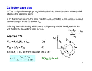
![Collector base bias
Advantages:
Better stabilization compared to fixed bias
Disadvantages:
This circuit provides negative feedback which reduces the gain of the amplifier.
Usage:
The feedback also decreases the input impedance of the amplifier as seen from
the base, which can be advantageous. Due to the gain reduction from feedback, this
biasing form is used only when the trade-off for stability is warranted.
8
How the bias stability is improved in collector base bias?
If IC becomes larger than design value, it causes an increase voltage drop
across RC hence smaller value of VCE which in turn causes IB to be smaller than
its design value. Since IC = βIB thus IC will also tend to be reduced towards its
original value.
biasing form is used only when the trade-off for stability is warranted.
]
)1(
[
CB
BECC
C
RR
VV
I
β
β
++
−
=
C
BECC
C
R
VV
I
−
=If RB<< βRC
For bais Stabilization : RB<< βRC](https://image.slidesharecdn.com/lec-7-151121060241-lva1-app6892/85/Analog-Digital-Electronics-8-320.jpg)


This document discusses different biasing schemes for BJTs, including fixed bias, collector base bias, and voltage divider bias. It explains how each biasing scheme works, its advantages and disadvantages, typical applications, and how stability is achieved. The key points are: 1) Different biasing schemes like fixed bias, collector base bias and voltage divider bias are used to set the operating point of BJTs and provide stability against variations in temperature, transistor parameters etc. 2) Collector base bias provides better stability than fixed bias by using negative feedback, but it reduces gain. Voltage divider bias is most widely used as it provides both stable biasing and high gain. 3) Stability is improved by


![Chp1 1 bjt [read only]](https://cdn.slidesharecdn.com/ss_thumbnails/chp11bjtread-only-130929091550-phpapp02-thumbnail.jpg?width=640&height=640&fit=bounds)