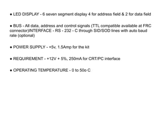
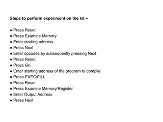
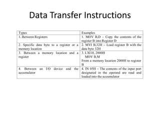
8085 Microprocessor
System Specifications -
● CPU - 8 bit Microprocessor, the 8085
● MEMORY - Total on board capacity of 64K bytes RAM - 8K/32K bytes and
space for further expansion
● ROM - 8K bytes of EPROM loaded with powerful program
● TIMER - 16 bit programmable timer / counter using 8253 I/O – 24
● I/O lines using 8255
● KEYBOARD - 10 keys for command 16 keys for hexadecimal data entry 1
key for vector interrupt & 1 key for reset
● LED DISPLAY - 6 seven segment display 4 for address field & 2 for data field
● BUS - All data, address and control signals (TTL compatible available at FRC
connector)INTERFACE - RS - 232 - C through SID/SOD lines with auto baud
rate (optional)
● POWER SUPPLY - +5v, 1.5Amp for the kit
● REQUIREMENT - +12V + 5%, 250mA for CRT/PC interface
● OPERATING TEMPERATURE - 0 to 50o C
8085 Microprocessor Trainer Kit
Steps to perform experiment on the kit –
● Press Reset
● Press Examine Memory
● Enter starting address
● Press Next
● Enter opcodes by subsequently pressing Next
● Press Reset
● Press Go
● Enter starting address of the program to compile
● Press EXEC/FILL
● Press Reset
● Press Examine Memory/Register
● Enter Output Address
● Press Next
8085 Architecture
ALU
• The ALU performs the following arithmetic and logical
operations.
– Addition
– Subtraction
– Logical AND
– Logical OR
– Logical EXCLUSIVE OR
– Complement (logical NOT)
– Increment (add 1)
– Decrement (subtract 1)
– Left shift
– Clear
Register Set
General Registers
• The 8085 has six general-purpose registers B, C, D, E, H,
and L
• They can be combined as register pairs - BC, DE, and HL -
to perform some 16-bit operations
• Registers can store or copy data into the registers by
using data copy instructions
• The HL register pair is also used to address memory
locations
Internally 8085 specifies these registers using 0s and 1s
only. So3-bits represent a register. The 3-bit register codes
for the registers of 8085:
Register Register code
B 000
C 001
D 010
E 011
H 100
L 101
M
(Data)
110
A 111
Using these binary codes, hex-codes against mnemonics
are formed. For example:
The opcode for MOV E, H − To represent MOV we are
having 2-bits 01 and rest 6-bits to represent 2 registers
destination and source against 3-bits each.
MOV E, H will have the hex-code as 0 1 0 1 1 1 0 0 => 5C
The opcode for MOV A, B − To represent MOV we are
having 2-bits 01 and rest 6-bits to represent 2registers
destination and source against 3-bits each.
MOV A, B will have the hex-code as 0 1 1 1 1 0 0 0 => 78
The opcode for MVI E, data − To represent
MVI we are having 2-bits 00
MVI E, M will have the hex-code as 0 0 0 1
1 1 1 0 => 1E
Accumulator & Pointers
• The accumulator is an 8-bit register that is a
part of arithmetic/logic unit (ALU)
• Program Counter – store address of next
instruction.
• Stack Pointer – store the address of stacktop
Instruction Register/Decoder
• The instruction register and the decoder are
considered as a part of the ALU
• The instruction register stores address of the
current instruction of a program
• The decoder decodes the instruction
Flags
• The ALU includes five flip-flops, which are set
or reset after an operation
• They are called Zero (Z), Carry (CY), Sign (S),
Parity (P), and Auxiliary Carry (AC) flags
Flags
• If the sum in the accumulator is larger than
eight bits then Carry flag (CY) – is set to one
• When an arithmetic operation results in zero,
then Zero (Z) flag is set to one
Flags
• The conditions (set or reset) of the flags are tested
through the software instructions
• The combination of the flag register and the accumulator
is called Program Status Word (PSW) and PSW is the 16-
bit unit for stack operation
Flags
Pin Diagram
Address & Data Bus
• Address Bus
• The 8085 has eight signal lines, A15-A8, which
are unidirectional and used as the high order
address bus
• Multiplexed Address/Data Bus
• The signal lines AD7-AD0 are bidirectional
• They serve a dual purpose
Address & Data Bus
• They are used as the low-order address bus as well as the
data bus
• In executing an instruction, during the earlier part of the
cycle, these lines are used as the low-order address bus
as well as the data bus
• During the later part of the cycle, these lines are used as
the data bus
• However the low order address bus can be separated
from these signals by using a latch
Addressing Modes
• 8-bit or 16-bit data may be directly given in the
instruction itself
• The address of the memory location, I/O port or I/O
device, where data resides, may be given in the
instruction itself
• In some instructions only one register is specified. The
content of the specified register is one of the operands.
Addressing Modes
• Some instructions specify one or two
registers. The contents of the registers are the
required data.
• In some instructions data is implied. The most
instructions of this type operate on the
content of the accumulator.
Addressing Modes
• Implicit addressing
 CMA (finds and stores the 1’s complement of
the contents of accumulator A in A)
 RRC (rotate accumulator A right by one bit)
 RLC (rotate accumulator A left by one bit)
 Immediate Addressing Mode –
The source operand is always data. If the
data is 8-bit, then the instruction will be of
2 bytes, if the data is of 16-bit then the
instruction will be of 3 bytes.
 MVI B 45 (move the data 45H immediately
to register B)
 LXI H 3050 (load the H-L pair with the
operand 3050H immediately)
 JMP address (jump to the operand
address immediately)
Direct Addressing Mode –
The data to be operated is available inside a
memory location and that memory location
is directly specified as an operand.
• LDA 2050 (load the contents of memory
location into accumulator A)
• LHLD address (load contents of 16-bit
memory location into H-L register pair)
Register addressing
The data to be operated is available inside
the register(s)
– In register addressing mode the operands are in
the general purpose registers
– MOV A, B
– ADD B
– LDAX B, STAX D
Register indirect addressing:
Memory location is specified by the contents of the
registers
• MOV A, M (move the contents of the memory
location pointed by the H-L pair to the
accumulator)
• LDAX B (move contents of B-C register to the
accumulator)
• LXIH 9570 (load immediate the H-L pair with the
address of the location 9570)
Instruction Formats
1. One-byte instructions –
In 1-byte instruction, the opcode and the operand of an
instruction are represented in one byte.
e.g. Copy the contents of accumulator in register B.
Mnemonic- MOV B, A
Opcode- MOV
Operand- B, A
Hex Code- 47H
Binary code- 0100 0111
2. Two-byte instructions –
Two-byte instruction is the type of instruction in which
the first 8 bits indicates the opcode and the next 8 bits
indicates the operand.
e.g. Load the hexadecimal data 32H in the accumulator.
Mnemonic- MVI A, 32H
Opcode- MVI
Operand- A, 32H
Hex Code- 3E
32
Binary code- 0011 1110
0011 0010
3. Three-byte instructions –
Three-byte instruction is the type of instruction in which the first
8 bits indicates the opcode and the next two bytes specify the
16-bit address. The low-order address is represented in second
byte and the high-order address is represented in the third byte.
e.g. Load contents of memory 2050H in the accumulator.
Mnemonic- LDA 2050H
Opcode- LDA
Operand- 2050H
Hex Code- 3A
50
20
Binary code- 0011 1010
0101 0000
0010 0000
8085 Instruction Set 32
Different Types of Instructions
Data Transfer Instructions
Types Examples
1. Between Registers 1. MOV B,D – Copy the contents of the
register B into Register D
2. Specific data byte to a register or a
memory location
2. MVI B,32H – Load register B with the
data byte 32H
3. Between a memory location and a
register
3. LXI H, 2000H
MOV B,M
From a memory location 2000H to register
B
4. Between an I/O device and the
accumulator
4. IN 05H – The contents of the input port
designated in the operand are read and
loaded into the accumulator
Arithmetic Instructions
• ADD B – [A] <----- [A]+[B]
• ADD M - [A] <----- [A]+[[HL]]
• DAD B – [HL] <----- [HL]+[BC]
• SUB C – [A] <----- [A]+[C]
• SUI 76H – [A] <---- [A]-76H
• SBB M – [A] <----- [A]-[[HL]]-[C]
Logical Instructions
• ANA C – [A] <----- [A] ^ [C]
• ANI 85H – [A] <----- [A] ^ 85H
• ORA M – [A] <----- [A] v [[HL]]
• XRA B – [A] <------ [A] XOR [B]
Rotate Instructions
• RLC
– [An+1] <----- [An]
– [A0] <------ [A7]
– [CS] <----- [A7]
• RAR
– [An] <------ [An+1]
– [CS] <------ [A0]
– [A7] <------ [CS]
Complement Instructions
• CMP R
• CPI data
Complement Instructions
• CMA – [A] <---- [A]’
• CMC – [CS] <----- [CS]’
Transfer Instructions
• JMP 2050H – [PC] <----- 2050H
• JZ 3100H – [PC] <----- 3100H if Z=1,
otherwise [PC] <----- [PC]+1
• JNC 4250H – [PC] <----- 4250H if C=0,
otherwise [PC] <----- [PC]+1
CALL & RET
• CALL Addr
• [[SP]-1] <------- [PCH]
• [[SP]-1] <------- [PCL]
• [SP] <----- [SP]-2
• [PC] <----- Addr
• RET
• [PCL] <------ [[SP]]
• [PCH] <------ [[SP]+1]
• [SP] <------ [SP]+2
Conversion and Execution
• Convert the mnemonics into Hex code; we
need to look up the code in 8085 instruction
set.
• Store the program in Read/Write memory of a
single-board microcomputer. This may require
the knowledge about memory addresses and
the output port addresses.
• Finally execute the program.

8085_Microprocessor(simar).ppt

  • 1.
    8085 Microprocessor System Specifications- ● CPU - 8 bit Microprocessor, the 8085 ● MEMORY - Total on board capacity of 64K bytes RAM - 8K/32K bytes and space for further expansion ● ROM - 8K bytes of EPROM loaded with powerful program ● TIMER - 16 bit programmable timer / counter using 8253 I/O – 24 ● I/O lines using 8255 ● KEYBOARD - 10 keys for command 16 keys for hexadecimal data entry 1 key for vector interrupt & 1 key for reset
  • 2.
    ● LED DISPLAY- 6 seven segment display 4 for address field & 2 for data field ● BUS - All data, address and control signals (TTL compatible available at FRC connector)INTERFACE - RS - 232 - C through SID/SOD lines with auto baud rate (optional) ● POWER SUPPLY - +5v, 1.5Amp for the kit ● REQUIREMENT - +12V + 5%, 250mA for CRT/PC interface ● OPERATING TEMPERATURE - 0 to 50o C
  • 3.
  • 4.
    Steps to performexperiment on the kit – ● Press Reset ● Press Examine Memory ● Enter starting address ● Press Next ● Enter opcodes by subsequently pressing Next ● Press Reset ● Press Go ● Enter starting address of the program to compile ● Press EXEC/FILL ● Press Reset ● Press Examine Memory/Register ● Enter Output Address ● Press Next
  • 5.
  • 6.
    ALU • The ALUperforms the following arithmetic and logical operations. – Addition – Subtraction – Logical AND – Logical OR – Logical EXCLUSIVE OR – Complement (logical NOT) – Increment (add 1) – Decrement (subtract 1) – Left shift – Clear
  • 7.
  • 8.
    General Registers • The8085 has six general-purpose registers B, C, D, E, H, and L • They can be combined as register pairs - BC, DE, and HL - to perform some 16-bit operations • Registers can store or copy data into the registers by using data copy instructions • The HL register pair is also used to address memory locations
  • 9.
    Internally 8085 specifiesthese registers using 0s and 1s only. So3-bits represent a register. The 3-bit register codes for the registers of 8085: Register Register code B 000 C 001 D 010 E 011 H 100 L 101 M (Data) 110 A 111
  • 10.
    Using these binarycodes, hex-codes against mnemonics are formed. For example: The opcode for MOV E, H − To represent MOV we are having 2-bits 01 and rest 6-bits to represent 2 registers destination and source against 3-bits each. MOV E, H will have the hex-code as 0 1 0 1 1 1 0 0 => 5C The opcode for MOV A, B − To represent MOV we are having 2-bits 01 and rest 6-bits to represent 2registers destination and source against 3-bits each. MOV A, B will have the hex-code as 0 1 1 1 1 0 0 0 => 78
  • 11.
    The opcode forMVI E, data − To represent MVI we are having 2-bits 00 MVI E, M will have the hex-code as 0 0 0 1 1 1 1 0 => 1E
  • 12.
    Accumulator & Pointers •The accumulator is an 8-bit register that is a part of arithmetic/logic unit (ALU) • Program Counter – store address of next instruction. • Stack Pointer – store the address of stacktop
  • 13.
    Instruction Register/Decoder • Theinstruction register and the decoder are considered as a part of the ALU • The instruction register stores address of the current instruction of a program • The decoder decodes the instruction
  • 14.
    Flags • The ALUincludes five flip-flops, which are set or reset after an operation • They are called Zero (Z), Carry (CY), Sign (S), Parity (P), and Auxiliary Carry (AC) flags
  • 15.
    Flags • If thesum in the accumulator is larger than eight bits then Carry flag (CY) – is set to one • When an arithmetic operation results in zero, then Zero (Z) flag is set to one
  • 16.
    Flags • The conditions(set or reset) of the flags are tested through the software instructions • The combination of the flag register and the accumulator is called Program Status Word (PSW) and PSW is the 16- bit unit for stack operation
  • 17.
  • 18.
  • 19.
    Address & DataBus • Address Bus • The 8085 has eight signal lines, A15-A8, which are unidirectional and used as the high order address bus • Multiplexed Address/Data Bus • The signal lines AD7-AD0 are bidirectional • They serve a dual purpose
  • 20.
    Address & DataBus • They are used as the low-order address bus as well as the data bus • In executing an instruction, during the earlier part of the cycle, these lines are used as the low-order address bus as well as the data bus • During the later part of the cycle, these lines are used as the data bus • However the low order address bus can be separated from these signals by using a latch
  • 21.
    Addressing Modes • 8-bitor 16-bit data may be directly given in the instruction itself • The address of the memory location, I/O port or I/O device, where data resides, may be given in the instruction itself • In some instructions only one register is specified. The content of the specified register is one of the operands.
  • 22.
    Addressing Modes • Someinstructions specify one or two registers. The contents of the registers are the required data. • In some instructions data is implied. The most instructions of this type operate on the content of the accumulator.
  • 23.
    Addressing Modes • Implicitaddressing  CMA (finds and stores the 1’s complement of the contents of accumulator A in A)  RRC (rotate accumulator A right by one bit)  RLC (rotate accumulator A left by one bit)
  • 24.
     Immediate AddressingMode – The source operand is always data. If the data is 8-bit, then the instruction will be of 2 bytes, if the data is of 16-bit then the instruction will be of 3 bytes.  MVI B 45 (move the data 45H immediately to register B)  LXI H 3050 (load the H-L pair with the operand 3050H immediately)  JMP address (jump to the operand address immediately)
  • 25.
    Direct Addressing Mode– The data to be operated is available inside a memory location and that memory location is directly specified as an operand. • LDA 2050 (load the contents of memory location into accumulator A) • LHLD address (load contents of 16-bit memory location into H-L register pair)
  • 26.
    Register addressing The datato be operated is available inside the register(s) – In register addressing mode the operands are in the general purpose registers – MOV A, B – ADD B – LDAX B, STAX D
  • 27.
    Register indirect addressing: Memorylocation is specified by the contents of the registers • MOV A, M (move the contents of the memory location pointed by the H-L pair to the accumulator) • LDAX B (move contents of B-C register to the accumulator) • LXIH 9570 (load immediate the H-L pair with the address of the location 9570)
  • 28.
  • 29.
    1. One-byte instructions– In 1-byte instruction, the opcode and the operand of an instruction are represented in one byte. e.g. Copy the contents of accumulator in register B. Mnemonic- MOV B, A Opcode- MOV Operand- B, A Hex Code- 47H Binary code- 0100 0111
  • 30.
    2. Two-byte instructions– Two-byte instruction is the type of instruction in which the first 8 bits indicates the opcode and the next 8 bits indicates the operand. e.g. Load the hexadecimal data 32H in the accumulator. Mnemonic- MVI A, 32H Opcode- MVI Operand- A, 32H Hex Code- 3E 32 Binary code- 0011 1110 0011 0010
  • 31.
    3. Three-byte instructions– Three-byte instruction is the type of instruction in which the first 8 bits indicates the opcode and the next two bytes specify the 16-bit address. The low-order address is represented in second byte and the high-order address is represented in the third byte. e.g. Load contents of memory 2050H in the accumulator. Mnemonic- LDA 2050H Opcode- LDA Operand- 2050H Hex Code- 3A 50 20 Binary code- 0011 1010 0101 0000 0010 0000
  • 32.
  • 33.
    Different Types ofInstructions
  • 34.
    Data Transfer Instructions TypesExamples 1. Between Registers 1. MOV B,D – Copy the contents of the register B into Register D 2. Specific data byte to a register or a memory location 2. MVI B,32H – Load register B with the data byte 32H 3. Between a memory location and a register 3. LXI H, 2000H MOV B,M From a memory location 2000H to register B 4. Between an I/O device and the accumulator 4. IN 05H – The contents of the input port designated in the operand are read and loaded into the accumulator
  • 35.
    Arithmetic Instructions • ADDB – [A] <----- [A]+[B] • ADD M - [A] <----- [A]+[[HL]] • DAD B – [HL] <----- [HL]+[BC] • SUB C – [A] <----- [A]+[C] • SUI 76H – [A] <---- [A]-76H • SBB M – [A] <----- [A]-[[HL]]-[C]
  • 36.
    Logical Instructions • ANAC – [A] <----- [A] ^ [C] • ANI 85H – [A] <----- [A] ^ 85H • ORA M – [A] <----- [A] v [[HL]] • XRA B – [A] <------ [A] XOR [B]
  • 37.
    Rotate Instructions • RLC –[An+1] <----- [An] – [A0] <------ [A7] – [CS] <----- [A7] • RAR – [An] <------ [An+1] – [CS] <------ [A0] – [A7] <------ [CS]
  • 38.
  • 39.
    Complement Instructions • CMA– [A] <---- [A]’ • CMC – [CS] <----- [CS]’
  • 40.
    Transfer Instructions • JMP2050H – [PC] <----- 2050H • JZ 3100H – [PC] <----- 3100H if Z=1, otherwise [PC] <----- [PC]+1 • JNC 4250H – [PC] <----- 4250H if C=0, otherwise [PC] <----- [PC]+1
  • 41.
    CALL & RET •CALL Addr • [[SP]-1] <------- [PCH] • [[SP]-1] <------- [PCL] • [SP] <----- [SP]-2 • [PC] <----- Addr • RET • [PCL] <------ [[SP]] • [PCH] <------ [[SP]+1] • [SP] <------ [SP]+2
  • 42.
    Conversion and Execution •Convert the mnemonics into Hex code; we need to look up the code in 8085 instruction set. • Store the program in Read/Write memory of a single-board microcomputer. This may require the knowledge about memory addresses and the output port addresses. • Finally execute the program.