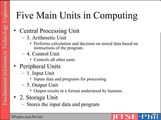
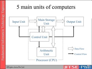
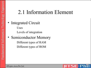
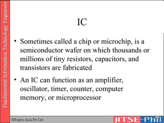
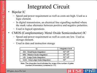
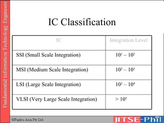
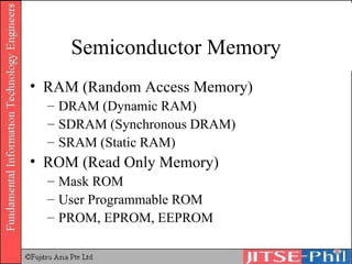
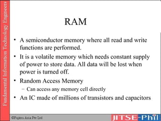
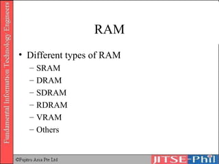
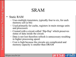
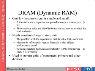
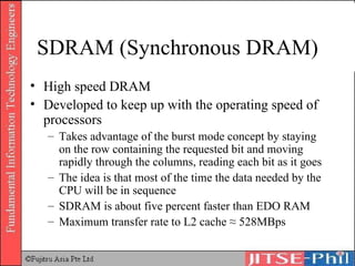
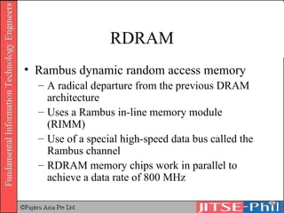
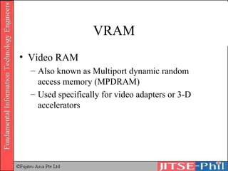
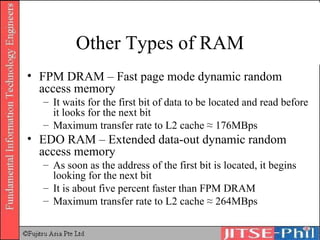
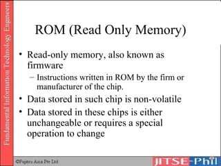
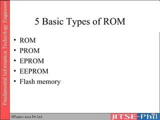
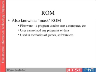
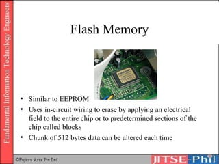
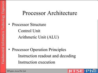
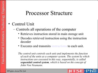
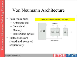
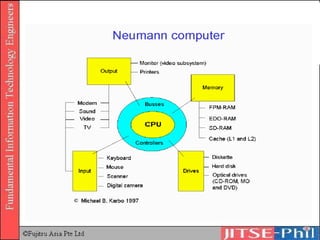
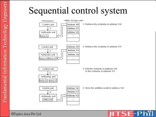
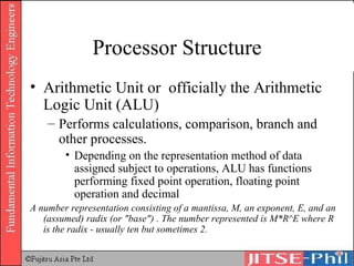
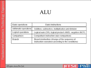
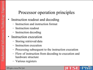
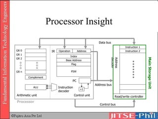
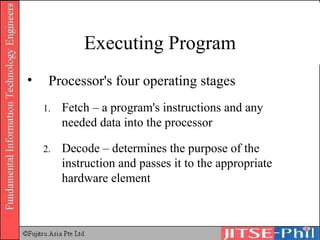
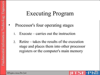
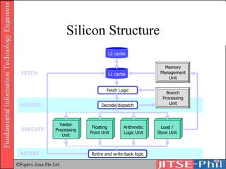
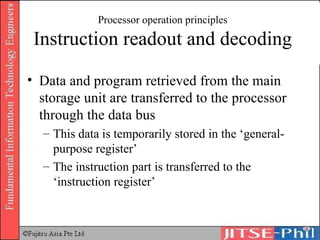
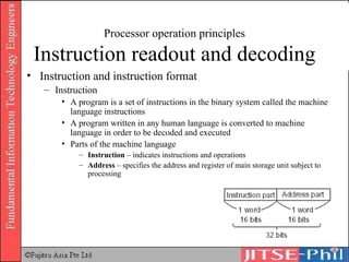
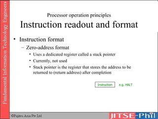
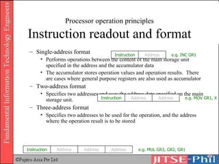
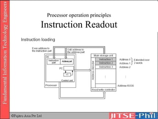
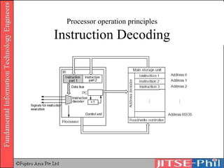
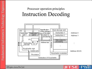
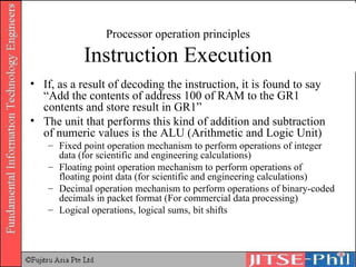
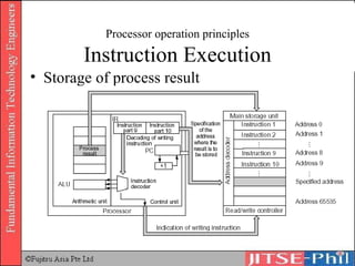
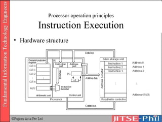
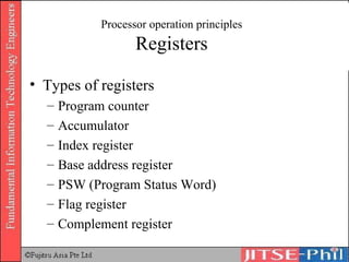
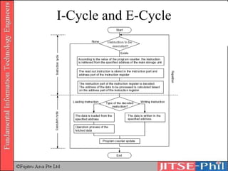
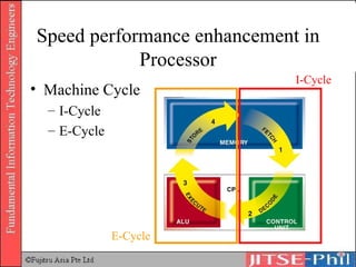
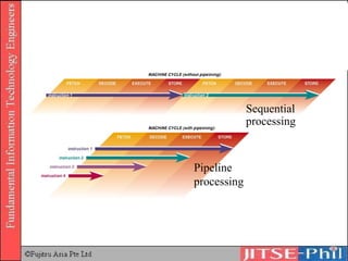
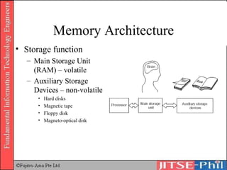
Part 1 Computer Systems Hardware (Book No. 1 Chapter 2)
HARDWARE 2.1 Information element 2.2 Processor architecture 2.3 Memory architecture 2.4 Auxiliary storage devices 2.5 Input/output architecture and devices
Introduction Functions of hardware in a computer can be divided into five main units
Five Main Units in Computing Central Processing Unit 3. Arithmetic Unit Performs calculation and decision on stored data based on instructions of the program. 4. Control Unit Controls all other units Peripheral Units 1. Input Unit Inputs data and programs for processing. 5. Output Unit Output results in a format understood by humans. 2. Storage Unit Stores the input data and program
5 main units of computers Input Unit Main Storage Unit Output Unit Arithmetic Unit Control Unit Processor (CPU) Data Flow Control Flow
2.1 Information Element Integrated Circuit Uses Levels of integration Semiconductor Memory Different types of RAM Different types of ROM
IC Sometimes called a chip or microchip, is a semiconductor wafer on which thousands or millions of tiny resistors, capacitors, and transistors are fabricated An IC can function as an amplifier, oscillator, timer, counter, computer memory, or microprocessor
Integrated Circuit Bipolar IC Speed and power requirement as well as costs are high. Used as a logic element. In digital transmission, an electrical line signalling method where the mark value alternates between positive and negative polarities. Used in logical operations CMOS (Complementary Metal Oxide Semiconductor) IC Speed and power requirement as well as costs are low. Used as storage element. Used in data and instruction storage
IC Classification > 10 5 VLSI (Very Large Scale Integration) 10 3  – 10 4 LSI (Large Scale Integration) 10 2  – 10 3 MSI (Medium Scale Integration) 10 1  – 10 2 SSI (Small Scale Integration) Integration Level IC
Transistors Per IC
Fujitsu Integrated Circuits 86903-33   Full die shot of the Fujitsu 86903-33 showing the complete pad ring using oblique illumination with blue, red, and yellow gels.
Sun Microsystems Integrated Circuits UltraSPARC Full die shot of the Sun Microsystems UltraSPARC microprocessor showing the complete pad ring using oblique illumination with red, blue, and yellow gels.
Intel Integrated Circuits i4004 Full die shot of the Intel i4004 microprocessor showing the complete pad with chip identifier, Intel logo, and bus connections using oblique illumination with blue, red, and yellow gels.
Semiconductor Memory RAM (Random Access Memory) DRAM (Dynamic RAM) SDRAM (Synchronous DRAM) SRAM (Static RAM) ROM (Read Only Memory) Mask ROM User Programmable ROM PROM, EPROM, EEPROM
RAM A semiconductor memory where all read and write functions are performed. It is a volatile memory which needs constant supply of power to store data. All data will be lost when power is turned off. Random Access Memory Can access any memory cell directly An IC made of millions of transistors and capacitors
RAM Different types of RAM SRAM DRAM SDRAM RDRAM VRAM Others
SRAM Static RAM Uses multiple transistors, typically four to six, for each memory cell (a bit) Used primarily for cache, registers in main storage units and processors Created with a circuit called ‘flip-flop’ which preserves status of data inside the circuit.  Data is not lost therefore refresh is unnecessary resulting in higher processing speed. Cost is high because the circuits are complicated and memory capacity is smaller than DRAM
DRAM (Dynamic RAM) Cost low because circuit is simple and small A transistor and a capacitor are paired to create a memory cell (a bit) The capacitor holds the bit of information and acts as a switch for read and write Needs constant charge to store data The problem with the capacitor is that its value leaks with time Memory is refreshed at regular intervals which affects performance speed Refresh operation happens automatically 1000s of times/sec – as such, it is ‘dynamic’ Used in storage units of computers, printers and other devices
SDRAM (Synchronous DRAM) High speed DRAM Developed to keep up with the operating speed of processors Takes advantage of the burst mode concept by staying on the row containing the requested bit and moving rapidly through the columns, reading each bit as it goes The idea is that most of the time the data needed by the CPU will be in sequence SDRAM is about five percent faster than EDO RAM Maximum transfer rate to L2 cache ≈ 528MBps
RDRAM Rambus dynamic random access memory A radical departure from the previous DRAM architecture Uses a Rambus in-line memory module (RIMM) Use of a special high-speed data bus called the Rambus channel RDRAM memory chips work in parallel to achieve a data rate of 800 MHz
VRAM Video RAM Also known as Multiport dynamic random access memory (MPDRAM) Used specifically for video adapters or 3-D accelerators
Other Types of RAM FPM DRAM – Fast page mode dynamic random access memory It waits for the first bit of data to be located and read before it looks for the next bit Maximum transfer rate to L2 cache ≈ 176MBps EDO RAM – Extended data-out dynamic random access memory As soon as the address of the first bit is located, it begins looking for the next bit It is about five percent faster than FPM DRAM Maximum transfer rate to L2 cache ≈ 264MBps
ROM (Read Only Memory) Read-only memory, also known as firmware Instructions written in ROM by the firm or manufacturer of the chip. Data stored in such chip is non-volatile Data stored in these chips is either unchangeable or requires a special operation to change
5 Basic Types of ROM ROM PROM EPROM EEPROM Flash memory
ROM Also known as ‘mask’ ROM Firmware – a program used to start a computer, etc User cannot add any programs or data Used in memories of games, software etc.
PROM Has a grid of columns and rows just as ordinary ROM Every intersection of a column and row has a fuse connecting them The higher voltage breaks the connection between the column and row by burning out the fuse
PROM Programmable read-only memory can only be programmed once Inexpensive Great for prototyping the data for a ROM before committing to the costly ROM fabrication process
EPROM Erasable programmable read-only memory Can be rewritten many times Similar to PROM, except that the intersection can be charged to create barrier for signal transmission Incremental changes cannot be done Ultraviolet light is used to erase the chip
EEPROM Electrically erasable programmable read-only memory Incremental changes can be done Electric field is used to alter the data Slow as only one byte can be changed each time
Flash Memory Similar to EEPROM Uses in-circuit wiring to erase by applying an electrical field to the entire chip or to predetermined sections of the chip called blocks Chunk of 512 bytes data can be altered each time
Processor Architecture Processor Structure Control Unit Arithmetic Unit (ALU) Processor Operation Principles Instruction readout and decoding Instruction execution
Processor Structure The CPU is the backbone of the computer, often compared to the human brain.  It consists of the control unit and the arithmetic unit.
Processor Structure Control Unit Controls all operations of the computer Retrieves instruction stored in main storage unit Decodes retrieved instruction using the instruction decoder Executes and transmits  instructions  to each unit.  The control unit controls each unit and implements the function of each of the units as a computer system. The system by which instructions are executed in this way, sequentially, is called  sequential control system , which is based on the concept of John Von Neumann.
Clock Speed
Von Neumann Architecture Four main parts Arithmetic unit Control unit Memory Input/Output devices Instructions are stored and executed sequentially
 
Sequential control system
Processor Structure Arithmetic Unit or  officially the Arithmetic Logic Unit (ALU) Performs calculations, comparison, branch and other processes.  Depending on the representation method of data assigned subject to operations, ALU has functions performing fixed point operation, floating point operation and decimal A number representation consisting of a mantissa, M, an exponent, E, and an (assumed) radix (or "base") . The number represented is M*R^E where R is the radix - usually ten but sometimes 2.
ALU
Processor operation principles Instruction readout and decoding Instruction and instruction format Instruction readout Instruction decoding Instruction execution Storing retrieved data Instruction execution Processing subsequent to the instruction execution Flow of instruction from decoding to execution and hardware structure Various registers
Processor Insight Instruction 1 Instruction 2 Read/write controller Address decoder Main Storage Unit ALU GR 0 GR 1 GR 2 GR n Instruction decoder Operation Address +1 Control unit Arithmetic unit PC IR Control bus Address bus Data bus Processor Base Address Flag PSW Index Complement
Executing Program Processor's four operating stages Fetch – a program's instructions and any needed data into the processor Decode – determines the purpose of the instruction and passes it to the appropriate hardware element
Executing Program Processor's four operating stages Execute – carries out the instruction Retire – takes the results of the execution stage and places them into other processor registers or the computer's main memory
Clock An important part of a microprocessor is its built-in clock, which determines the maximum speed at which other units can operate and helps synchronize related operations 2 GHz ≈ 2 billion clock cycles per second
Silicon Structure Fetch Logic Decode/dispatch L2 cache L1 cache Vector Processing Unit Floating Point Unit Arithmetic Logic Unit Load / Store Unit Retire and write-back logic Memory Management Unit Branch Processing Unit FETCH DECODE EXECUTE RETIRE
Processor operation principles Instruction readout and decoding Data and program retrieved from the main storage unit are transferred to the processor through the data bus This data is temporarily stored in the ‘general-purpose register’ The instruction part is transferred to the ‘instruction register’
Processor operation principles Instruction readout and decoding Instruction  and instruction format Instruction A program is a set of instructions in the binary system called the machine language instructions A program written in any human language is converted to machine language in order to be decoded and executed Parts of the machine language Instruction  – indicates instructions and operations Address  – specifies the address and register of main storage unit subject to processing
Processor operation principles Instruction readout and format Instruction format Zero-address format Uses a dedicated register called a stack pointer Currently, not used Stack pointer is the register that stores the address to be returned to (return address) after completion Instruction e.g. HALT
Processor operation principles Instruction readout and format Single-address format Performs operations between the content of the main storage unit specified in the address and the accumulator data The accumulator stores operation values and operation results.  There are cases where general purpose registers are also used as accumulator Two-address format Specifies two addresses and uses the address data specified on the main storage unit. Three-address format Specifies two addresses to be used for the operation, and the address where the operation result is to be stored Instruction Address e.g. INC GR1 Instruction Address Address e.g. MOV GR1, X Instruction Address Address Address e.g. MUL GR3, GR2, GR1
Processor operation principles Instruction Readout
Processor operation principles Instruction Decoding Content of instruction part of instruction register is transferred to a decoder. Decoder decodes the instruction and sends signals for the execution of the operation to each unit Content of the address part is transferred to the address bus
Processor operation principles Instruction Decoding
Processor operation principles Instruction Execution Once the instruction content and address of the data are obtained, the instruction is executed.
Processor operation principles Instruction Execution Storing retrieved data If, as a result of decoding the instruction part and the address part using the instruction decoder, the instruction is found to say "Retrieve and transfer to the processor the contents of address 100 of the main storage unit," a place to store the retrieved contents will be needed.  Therefore, a general-purpose register is set in the arithmetic unit of the processor in order to store the retrieved data.  In this example, it is assumed that there are five registers, and, for convenience, the numbers 0 to 4 will be assigned to them. Then, using the initials of each of the general-purpose registers, they will be represented as GR0, GR1, GR2, GR3 and GR4.
Processor operation principles Instruction Execution General-purpose registers
Processor operation principles Instruction Execution Contents of address 100 of the main storage unit (RAM) passes through the data bus to be stored in general-purpose register GR1
Processor operation principles Instruction Execution If, as a result of decoding the instruction, it is found to say “Add the contents of address 100 of RAM to the GR1 contents and store result in GR1” The unit that performs this kind of addition and subtraction of numeric values is the ALU (Arithmetic and Logic Unit) Fixed point operation mechanism to perform operations of integer data (for scientific and engineering calculations) Floating point operation mechanism to perform operations of floating point data (for scientific and engineering calculations) Decimal operation mechanism to perform operations of binary-coded decimals in packet format (For commercial data processing) Logical operations, logical sums, bit shifts
Processor operation principles Instruction Execution Storage of process result
Processor operation principles Instruction Execution Hardware structure
Processor operation principles Registers Types of registers Program counter Accumulator Index register Base address register PSW (Program Status Word) Flag register Complement register
Register Program Counter (PC) A specialized register within the processor When computer boots up, the content of the program counter is immediately read and the address of the main storage unit to be accessed is verified. “ Load instruction A stored in address 101 of the RAM into the processor”
Register  Accumulator Used to exclusively store operation results and values There are cases where the general-purpose register is used as a substitute for the accumulator Accumulator mode: When the accumulator is used. General purpose mode: When a general purpose register is used as a substitute for the accumulator
Register Index Register Performs address modification Changes address part of the instruction when an address in the main storage unit is specified.
Register Base register Stores the program top address
Register Flag register Stores information related to operation result to the existence of carry, overflow, etc
Register Program Status Word (PWS) The program counter, flag register and other information are registered in the PWS. If an event interrupts the program in the processor, the program execution can be resumed using the PWS information
Register Complement Register Generates integer complements in order to perform operations in the addition circuit
Address specification mode Address part of instruction specifies main storage unit address and the register subject to be processed This address is not used during instruction execution. The actual address is specified after performing calculations between the specified register and the addresses This operation is called address modification Actual address obtained is called the “effective address”
Address specification mode Immediate specification  Direct address specification Index address specification Register address specification Base address specification Relative address specification Indirect address specification
Immediate Specification Data is contained in the address part, can be executed immediately
Direct address specification Address of data is contained in the address part
Index address specification The address part is divided into the section that specifies the number of the index register and the constant section, and the effective address is the result of the following addition:  (Content of the register content specified with the register number) + (Address constant)
Register Address Specification Register number stored in address part Address is stored in register of that number
Base address specification The program starting address is stored in the base register The result of the addition of the address in the base register and the address constant becomes the effective address
Relative address specification Result of the address of instruction being executed and the address of the address part become the effective address
Indirect address specification Address of data is contained in the address specified in the address part May be performed on two or three levels
Processor operation principles Instruction Set When user inputs request, the software interacts with the hardware to process the instructions built into the computer. This group of instruction is called the instruction set Depending on the computer, the types and number of instructions differ Computer software packages with identical instruction sets are basically compatible OS/2 Warp (Win OS/2 packaged) Execution control of the instruction Repetition of readout of instruction from main storage unit  Decoding and execution of instruction by control unit * Instruction readout (I-cycle or Fetch cycle) * Instruction execution (E-cycle)
I-Cycle and E-Cycle
Speed performance enhancement in Processor Machine Cycle I-Cycle E-Cycle I-Cycle E-Cycle
Sequential processing Pipeline  processing
Instruction Set Instructions are executed by the mico-program Complex, high level type instructions Variation in the instruction size and length of execution Complex Instruction Set Computer (CISC) Instructions are executed by the hardware Basic instructions About the same in the instruction size and length of execution Reduced Instruction Set Computer (RISC)
Parallel method Using multiple processors simultaneously to execute a program Speeds execution Requires special system software
Parallel method
Multi-processor Designed to improve performance and reliability of the system Multiple processors in parallel with each processor having a dedicated function Fault-tolerance Resource-sharing
Parallel Processing Super scalar architecture Super pipeline architecture Instruction 1 F D E R Instruction 3 F D E R Instruction 5 F D E R Instruction 2 F D E R Instruction 4 F D E R Instruction 6 F D E R Instruction 1 F' F" D' D" E' E" R' R" Instruction 2 F' F" D' D" E' E" R' R" Instruction 3 F' F" D' D" E' E" R' R" Instruction 4 F' F" D' D" E' E" R' R" Instruction 5 F' F" D' D" E' E" R' R" Instruction 6 F' F" D' D" E' E" R' R"
Multi-processor Symmetric Multi-processor memory  is shared among all the processors executing the same OS.  Competition for the use of memory limits number of processors that can be connected. Array processor High speed scientific computing using pipeline processing Large scale or dedicated mathematical processors Deploy pipeline processing principle Each unit (i.e. processor) is in a queue passing its completed result to the next unit Also known as vector processing
Parallel Processing Multiple processors cooperate with multiple tasks being performed to execute one job.   SISD (Single Instruction Single Data Stream) One instruction stream operating on a single data element and is not parallel SIMD (Single Instruction Multiple Data Stream) Each instruction may operate on more than one data element and is synchronous. Parallel SIMD The same instruction is executed by all processors operating on different sets of data. MIMD (Multiple Instruction Multiple Data Stream) Each processor has its own instruction stream acts on its own data stream independent of the other processors
Processor Performance Performance E.g. 500MHz = 500,000,000  pulses per sec Clock frequency = 1/500MHz = 2 n s per pulse CPI (Cycles Per Instruction) CPI ≈ number of clock ticks required to execute one instruction
Digital IC NOT gate AND gate OR gate XOR gate NAND gate NOR gate Half-adder Full-adder Flip-flop Digital IC Logic Gates Transistors Capacitors Diodes
' NOT '  Gate 0 1 1 0 NOT  A A A
' AND '  Gate 1 1 1 0 0 1 0 1 0 0 0 0 A  AND  B B A A B
' OR '  Gate 1 1 1 1 0 1 1 1 0 0 0 0 A  OR  B B A A B
'X OR '  Gate 0 1 1 1 0 1 1 1 0 0 0 0 A  XOR  B B A A B
'N AND '  Gate 0 1 1 1 0 1 1 1 0 1 0 0 A  NAND  B B A A B
'N OR '  Gate 0 1 1 0 0 1 0 1 0 1 0 0 A  NOR  B B A A B
Exercise 1 Construct the truth table for the following circuit A B C 1 1 1 0 0 1 0 1 0 1 0 0 C B A
Exercise 2 Construct the truth table for the following circuit a 1 a 0 L 1 L 2 L 3 L 4 0 0 0 1 1 1 0 0 1 0 0 1 0 1 0 0 1 0 1 0 0 0 0 0 L 4 L 3 L 2 L 1 a 0 a 1
Exercise 3 Construct the truth table for the following circuit S A B C 0 0 1 0 0 1 0 0 1 0 0 1 1 1 1 0 1 1 1 1 1 0 1 1 0 1 0 1 0 0 0 0 C S B A
Hardware Storage
Memory Architecture Storage function Main Storage Unit (RAM)  – volatile Auxiliary Storage Devices – non-volatile Hard disks Magnetic tape Floppy disk Magneto-optical disk
Memory Capacity and Performance Memory hierarchical structure Access time * Processor requests data readout * Processor selects main storage unit address with the address bus * Data of selected address is transferred through data bus Time taken for these processes to complete is called Access Time. Cycle Time * Refresh interval
Memory Hierarchy Structure
Memory Capacity
Memory Performance (Access Time) Time elapsed from when the processor sends the read/write instruction to the storage unit until the data delivery/acceptance is completed. For the processor to access the main storage unit data, the following three stages are necessary: The time during which the processor requests the data readout The time during which the processor selects the main storage unit address with the address bus The time during which the data of the selected address is transferred through the data bus. In other words,   +  +   represent the time elapsed from when the data access request is sent until the data transfer is completed. This lapse of time is called the  access time.
Memory Performance (Cycle Time) Among the storage elements of the storage unit, when data is to be stored in the capacitor, there are some whose memory fades with time, as with DRAM.  Refreshing operation  that rewrites data at regular intervals becomes necessary.  For that reason, after the data transfer is completed, a  preparation time  in order to receive the next request becomes necessary.  Cycle time = Access time + Preparation time
Cycle Time
Memory Configuration Memory used in the computer can be classified into hierarchies.  To provide for the occurrence of malfunctions or failures, these devices are equipped with data error detection and error correction functions.  Implemented by several Error Correcting Codes (ECC).
Error Correcting Codes (ECC) Magnetic disk  Errors caused by a small scratch (burst errors) Cyclic Redundancy Check (CRC) code to detect burst errors Magnetic tape 1 byte data in transverse direction Parity check system detecting odd number of bit errors appends vertical parity bits CRC code used to detect burst errors
ECC Main Memory Hamming code used to detect single-bit and double-bit errors. Memory protection system Access rights Read, Write, Execute Data (RW) Instructions (E) When violated, interrupt occurs and control passes to OS Boundary register system (a dedicated register specifies the addressable domain for each program)

11. Computer Systems Hardware 1

  • 1.
    Part 1 ComputerSystems Hardware (Book No. 1 Chapter 2)
  • 2.
    HARDWARE 2.1 Informationelement 2.2 Processor architecture 2.3 Memory architecture 2.4 Auxiliary storage devices 2.5 Input/output architecture and devices
  • 3.
    Introduction Functions ofhardware in a computer can be divided into five main units
  • 4.
    Five Main Unitsin Computing Central Processing Unit 3. Arithmetic Unit Performs calculation and decision on stored data based on instructions of the program. 4. Control Unit Controls all other units Peripheral Units 1. Input Unit Inputs data and programs for processing. 5. Output Unit Output results in a format understood by humans. 2. Storage Unit Stores the input data and program
  • 5.
    5 main unitsof computers Input Unit Main Storage Unit Output Unit Arithmetic Unit Control Unit Processor (CPU) Data Flow Control Flow
  • 6.
    2.1 Information ElementIntegrated Circuit Uses Levels of integration Semiconductor Memory Different types of RAM Different types of ROM
  • 7.
    IC Sometimes calleda chip or microchip, is a semiconductor wafer on which thousands or millions of tiny resistors, capacitors, and transistors are fabricated An IC can function as an amplifier, oscillator, timer, counter, computer memory, or microprocessor
  • 8.
    Integrated Circuit BipolarIC Speed and power requirement as well as costs are high. Used as a logic element. In digital transmission, an electrical line signalling method where the mark value alternates between positive and negative polarities. Used in logical operations CMOS (Complementary Metal Oxide Semiconductor) IC Speed and power requirement as well as costs are low. Used as storage element. Used in data and instruction storage
  • 9.
    IC Classification >10 5 VLSI (Very Large Scale Integration) 10 3 – 10 4 LSI (Large Scale Integration) 10 2 – 10 3 MSI (Medium Scale Integration) 10 1 – 10 2 SSI (Small Scale Integration) Integration Level IC
  • 10.
  • 11.
    Fujitsu Integrated Circuits86903-33 Full die shot of the Fujitsu 86903-33 showing the complete pad ring using oblique illumination with blue, red, and yellow gels.
  • 12.
    Sun Microsystems IntegratedCircuits UltraSPARC Full die shot of the Sun Microsystems UltraSPARC microprocessor showing the complete pad ring using oblique illumination with red, blue, and yellow gels.
  • 13.
    Intel Integrated Circuitsi4004 Full die shot of the Intel i4004 microprocessor showing the complete pad with chip identifier, Intel logo, and bus connections using oblique illumination with blue, red, and yellow gels.
  • 14.
    Semiconductor Memory RAM(Random Access Memory) DRAM (Dynamic RAM) SDRAM (Synchronous DRAM) SRAM (Static RAM) ROM (Read Only Memory) Mask ROM User Programmable ROM PROM, EPROM, EEPROM
  • 15.
    RAM A semiconductormemory where all read and write functions are performed. It is a volatile memory which needs constant supply of power to store data. All data will be lost when power is turned off. Random Access Memory Can access any memory cell directly An IC made of millions of transistors and capacitors
  • 16.
    RAM Different typesof RAM SRAM DRAM SDRAM RDRAM VRAM Others
  • 17.
    SRAM Static RAMUses multiple transistors, typically four to six, for each memory cell (a bit) Used primarily for cache, registers in main storage units and processors Created with a circuit called ‘flip-flop’ which preserves status of data inside the circuit. Data is not lost therefore refresh is unnecessary resulting in higher processing speed. Cost is high because the circuits are complicated and memory capacity is smaller than DRAM
  • 18.
    DRAM (Dynamic RAM)Cost low because circuit is simple and small A transistor and a capacitor are paired to create a memory cell (a bit) The capacitor holds the bit of information and acts as a switch for read and write Needs constant charge to store data The problem with the capacitor is that its value leaks with time Memory is refreshed at regular intervals which affects performance speed Refresh operation happens automatically 1000s of times/sec – as such, it is ‘dynamic’ Used in storage units of computers, printers and other devices
  • 19.
    SDRAM (Synchronous DRAM)High speed DRAM Developed to keep up with the operating speed of processors Takes advantage of the burst mode concept by staying on the row containing the requested bit and moving rapidly through the columns, reading each bit as it goes The idea is that most of the time the data needed by the CPU will be in sequence SDRAM is about five percent faster than EDO RAM Maximum transfer rate to L2 cache ≈ 528MBps
  • 20.
    RDRAM Rambus dynamicrandom access memory A radical departure from the previous DRAM architecture Uses a Rambus in-line memory module (RIMM) Use of a special high-speed data bus called the Rambus channel RDRAM memory chips work in parallel to achieve a data rate of 800 MHz
  • 21.
    VRAM Video RAMAlso known as Multiport dynamic random access memory (MPDRAM) Used specifically for video adapters or 3-D accelerators
  • 22.
    Other Types ofRAM FPM DRAM – Fast page mode dynamic random access memory It waits for the first bit of data to be located and read before it looks for the next bit Maximum transfer rate to L2 cache ≈ 176MBps EDO RAM – Extended data-out dynamic random access memory As soon as the address of the first bit is located, it begins looking for the next bit It is about five percent faster than FPM DRAM Maximum transfer rate to L2 cache ≈ 264MBps
  • 23.
    ROM (Read OnlyMemory) Read-only memory, also known as firmware Instructions written in ROM by the firm or manufacturer of the chip. Data stored in such chip is non-volatile Data stored in these chips is either unchangeable or requires a special operation to change
  • 24.
    5 Basic Typesof ROM ROM PROM EPROM EEPROM Flash memory
  • 25.
    ROM Also knownas ‘mask’ ROM Firmware – a program used to start a computer, etc User cannot add any programs or data Used in memories of games, software etc.
  • 26.
    PROM Has agrid of columns and rows just as ordinary ROM Every intersection of a column and row has a fuse connecting them The higher voltage breaks the connection between the column and row by burning out the fuse
  • 27.
    PROM Programmable read-onlymemory can only be programmed once Inexpensive Great for prototyping the data for a ROM before committing to the costly ROM fabrication process
  • 28.
    EPROM Erasable programmableread-only memory Can be rewritten many times Similar to PROM, except that the intersection can be charged to create barrier for signal transmission Incremental changes cannot be done Ultraviolet light is used to erase the chip
  • 29.
    EEPROM Electrically erasableprogrammable read-only memory Incremental changes can be done Electric field is used to alter the data Slow as only one byte can be changed each time
  • 30.
    Flash Memory Similarto EEPROM Uses in-circuit wiring to erase by applying an electrical field to the entire chip or to predetermined sections of the chip called blocks Chunk of 512 bytes data can be altered each time
  • 31.
    Processor Architecture ProcessorStructure Control Unit Arithmetic Unit (ALU) Processor Operation Principles Instruction readout and decoding Instruction execution
  • 32.
    Processor Structure TheCPU is the backbone of the computer, often compared to the human brain. It consists of the control unit and the arithmetic unit.
  • 33.
    Processor Structure ControlUnit Controls all operations of the computer Retrieves instruction stored in main storage unit Decodes retrieved instruction using the instruction decoder Executes and transmits instructions to each unit. The control unit controls each unit and implements the function of each of the units as a computer system. The system by which instructions are executed in this way, sequentially, is called sequential control system , which is based on the concept of John Von Neumann.
  • 34.
  • 35.
    Von Neumann ArchitectureFour main parts Arithmetic unit Control unit Memory Input/Output devices Instructions are stored and executed sequentially
  • 36.
  • 37.
  • 38.
    Processor Structure ArithmeticUnit or officially the Arithmetic Logic Unit (ALU) Performs calculations, comparison, branch and other processes. Depending on the representation method of data assigned subject to operations, ALU has functions performing fixed point operation, floating point operation and decimal A number representation consisting of a mantissa, M, an exponent, E, and an (assumed) radix (or "base") . The number represented is M*R^E where R is the radix - usually ten but sometimes 2.
  • 39.
  • 40.
    Processor operation principlesInstruction readout and decoding Instruction and instruction format Instruction readout Instruction decoding Instruction execution Storing retrieved data Instruction execution Processing subsequent to the instruction execution Flow of instruction from decoding to execution and hardware structure Various registers
  • 41.
    Processor Insight Instruction1 Instruction 2 Read/write controller Address decoder Main Storage Unit ALU GR 0 GR 1 GR 2 GR n Instruction decoder Operation Address +1 Control unit Arithmetic unit PC IR Control bus Address bus Data bus Processor Base Address Flag PSW Index Complement
  • 42.
    Executing Program Processor'sfour operating stages Fetch – a program's instructions and any needed data into the processor Decode – determines the purpose of the instruction and passes it to the appropriate hardware element
  • 43.
    Executing Program Processor'sfour operating stages Execute – carries out the instruction Retire – takes the results of the execution stage and places them into other processor registers or the computer's main memory
  • 44.
    Clock An importantpart of a microprocessor is its built-in clock, which determines the maximum speed at which other units can operate and helps synchronize related operations 2 GHz ≈ 2 billion clock cycles per second
  • 45.
    Silicon Structure FetchLogic Decode/dispatch L2 cache L1 cache Vector Processing Unit Floating Point Unit Arithmetic Logic Unit Load / Store Unit Retire and write-back logic Memory Management Unit Branch Processing Unit FETCH DECODE EXECUTE RETIRE
  • 46.
    Processor operation principlesInstruction readout and decoding Data and program retrieved from the main storage unit are transferred to the processor through the data bus This data is temporarily stored in the ‘general-purpose register’ The instruction part is transferred to the ‘instruction register’
  • 47.
    Processor operation principlesInstruction readout and decoding Instruction and instruction format Instruction A program is a set of instructions in the binary system called the machine language instructions A program written in any human language is converted to machine language in order to be decoded and executed Parts of the machine language Instruction – indicates instructions and operations Address – specifies the address and register of main storage unit subject to processing
  • 48.
    Processor operation principlesInstruction readout and format Instruction format Zero-address format Uses a dedicated register called a stack pointer Currently, not used Stack pointer is the register that stores the address to be returned to (return address) after completion Instruction e.g. HALT
  • 49.
    Processor operation principlesInstruction readout and format Single-address format Performs operations between the content of the main storage unit specified in the address and the accumulator data The accumulator stores operation values and operation results. There are cases where general purpose registers are also used as accumulator Two-address format Specifies two addresses and uses the address data specified on the main storage unit. Three-address format Specifies two addresses to be used for the operation, and the address where the operation result is to be stored Instruction Address e.g. INC GR1 Instruction Address Address e.g. MOV GR1, X Instruction Address Address Address e.g. MUL GR3, GR2, GR1
  • 50.
    Processor operation principlesInstruction Readout
  • 51.
    Processor operation principlesInstruction Decoding Content of instruction part of instruction register is transferred to a decoder. Decoder decodes the instruction and sends signals for the execution of the operation to each unit Content of the address part is transferred to the address bus
  • 52.
    Processor operation principlesInstruction Decoding
  • 53.
    Processor operation principlesInstruction Decoding
  • 54.
    Processor operation principlesInstruction Execution Once the instruction content and address of the data are obtained, the instruction is executed.
  • 55.
    Processor operation principlesInstruction Execution Storing retrieved data If, as a result of decoding the instruction part and the address part using the instruction decoder, the instruction is found to say "Retrieve and transfer to the processor the contents of address 100 of the main storage unit," a place to store the retrieved contents will be needed. Therefore, a general-purpose register is set in the arithmetic unit of the processor in order to store the retrieved data. In this example, it is assumed that there are five registers, and, for convenience, the numbers 0 to 4 will be assigned to them. Then, using the initials of each of the general-purpose registers, they will be represented as GR0, GR1, GR2, GR3 and GR4.
  • 56.
    Processor operation principlesInstruction Execution General-purpose registers
  • 57.
    Processor operation principlesInstruction Execution Contents of address 100 of the main storage unit (RAM) passes through the data bus to be stored in general-purpose register GR1
  • 58.
    Processor operation principlesInstruction Execution If, as a result of decoding the instruction, it is found to say “Add the contents of address 100 of RAM to the GR1 contents and store result in GR1” The unit that performs this kind of addition and subtraction of numeric values is the ALU (Arithmetic and Logic Unit) Fixed point operation mechanism to perform operations of integer data (for scientific and engineering calculations) Floating point operation mechanism to perform operations of floating point data (for scientific and engineering calculations) Decimal operation mechanism to perform operations of binary-coded decimals in packet format (For commercial data processing) Logical operations, logical sums, bit shifts
  • 59.
    Processor operation principlesInstruction Execution Storage of process result
  • 60.
    Processor operation principlesInstruction Execution Hardware structure
  • 61.
    Processor operation principlesRegisters Types of registers Program counter Accumulator Index register Base address register PSW (Program Status Word) Flag register Complement register
  • 62.
    Register Program Counter(PC) A specialized register within the processor When computer boots up, the content of the program counter is immediately read and the address of the main storage unit to be accessed is verified. “ Load instruction A stored in address 101 of the RAM into the processor”
  • 63.
    Register AccumulatorUsed to exclusively store operation results and values There are cases where the general-purpose register is used as a substitute for the accumulator Accumulator mode: When the accumulator is used. General purpose mode: When a general purpose register is used as a substitute for the accumulator
  • 64.
    Register Index RegisterPerforms address modification Changes address part of the instruction when an address in the main storage unit is specified.
  • 65.
    Register Base registerStores the program top address
  • 66.
    Register Flag registerStores information related to operation result to the existence of carry, overflow, etc
  • 67.
    Register Program StatusWord (PWS) The program counter, flag register and other information are registered in the PWS. If an event interrupts the program in the processor, the program execution can be resumed using the PWS information
  • 68.
    Register Complement RegisterGenerates integer complements in order to perform operations in the addition circuit
  • 69.
    Address specification modeAddress part of instruction specifies main storage unit address and the register subject to be processed This address is not used during instruction execution. The actual address is specified after performing calculations between the specified register and the addresses This operation is called address modification Actual address obtained is called the “effective address”
  • 70.
    Address specification modeImmediate specification Direct address specification Index address specification Register address specification Base address specification Relative address specification Indirect address specification
  • 71.
    Immediate Specification Datais contained in the address part, can be executed immediately
  • 72.
    Direct address specificationAddress of data is contained in the address part
  • 73.
    Index address specificationThe address part is divided into the section that specifies the number of the index register and the constant section, and the effective address is the result of the following addition: (Content of the register content specified with the register number) + (Address constant)
  • 74.
    Register Address SpecificationRegister number stored in address part Address is stored in register of that number
  • 75.
    Base address specificationThe program starting address is stored in the base register The result of the addition of the address in the base register and the address constant becomes the effective address
  • 76.
    Relative address specificationResult of the address of instruction being executed and the address of the address part become the effective address
  • 77.
    Indirect address specificationAddress of data is contained in the address specified in the address part May be performed on two or three levels
  • 78.
    Processor operation principlesInstruction Set When user inputs request, the software interacts with the hardware to process the instructions built into the computer. This group of instruction is called the instruction set Depending on the computer, the types and number of instructions differ Computer software packages with identical instruction sets are basically compatible OS/2 Warp (Win OS/2 packaged) Execution control of the instruction Repetition of readout of instruction from main storage unit Decoding and execution of instruction by control unit * Instruction readout (I-cycle or Fetch cycle) * Instruction execution (E-cycle)
  • 79.
  • 80.
    Speed performance enhancementin Processor Machine Cycle I-Cycle E-Cycle I-Cycle E-Cycle
  • 81.
  • 82.
    Instruction Set Instructionsare executed by the mico-program Complex, high level type instructions Variation in the instruction size and length of execution Complex Instruction Set Computer (CISC) Instructions are executed by the hardware Basic instructions About the same in the instruction size and length of execution Reduced Instruction Set Computer (RISC)
  • 83.
    Parallel method Usingmultiple processors simultaneously to execute a program Speeds execution Requires special system software
  • 84.
  • 85.
    Multi-processor Designed toimprove performance and reliability of the system Multiple processors in parallel with each processor having a dedicated function Fault-tolerance Resource-sharing
  • 86.
    Parallel Processing Superscalar architecture Super pipeline architecture Instruction 1 F D E R Instruction 3 F D E R Instruction 5 F D E R Instruction 2 F D E R Instruction 4 F D E R Instruction 6 F D E R Instruction 1 F' F" D' D" E' E" R' R" Instruction 2 F' F" D' D" E' E" R' R" Instruction 3 F' F" D' D" E' E" R' R" Instruction 4 F' F" D' D" E' E" R' R" Instruction 5 F' F" D' D" E' E" R' R" Instruction 6 F' F" D' D" E' E" R' R"
  • 87.
    Multi-processor Symmetric Multi-processormemory  is shared among all the processors executing the same OS. Competition for the use of memory limits number of processors that can be connected. Array processor High speed scientific computing using pipeline processing Large scale or dedicated mathematical processors Deploy pipeline processing principle Each unit (i.e. processor) is in a queue passing its completed result to the next unit Also known as vector processing
  • 88.
    Parallel Processing Multipleprocessors cooperate with multiple tasks being performed to execute one job.   SISD (Single Instruction Single Data Stream) One instruction stream operating on a single data element and is not parallel SIMD (Single Instruction Multiple Data Stream) Each instruction may operate on more than one data element and is synchronous. Parallel SIMD The same instruction is executed by all processors operating on different sets of data. MIMD (Multiple Instruction Multiple Data Stream) Each processor has its own instruction stream acts on its own data stream independent of the other processors
  • 89.
    Processor Performance PerformanceE.g. 500MHz = 500,000,000 pulses per sec Clock frequency = 1/500MHz = 2 n s per pulse CPI (Cycles Per Instruction) CPI ≈ number of clock ticks required to execute one instruction
  • 90.
    Digital IC NOTgate AND gate OR gate XOR gate NAND gate NOR gate Half-adder Full-adder Flip-flop Digital IC Logic Gates Transistors Capacitors Diodes
  • 91.
    ' NOT ' Gate 0 1 1 0 NOT A A A
  • 92.
    ' AND ' Gate 1 1 1 0 0 1 0 1 0 0 0 0 A AND B B A A B
  • 93.
    ' OR ' Gate 1 1 1 1 0 1 1 1 0 0 0 0 A OR B B A A B
  • 94.
    'X OR ' Gate 0 1 1 1 0 1 1 1 0 0 0 0 A XOR B B A A B
  • 95.
    'N AND ' Gate 0 1 1 1 0 1 1 1 0 1 0 0 A NAND B B A A B
  • 96.
    'N OR ' Gate 0 1 1 0 0 1 0 1 0 1 0 0 A NOR B B A A B
  • 97.
    Exercise 1 Constructthe truth table for the following circuit A B C 1 1 1 0 0 1 0 1 0 1 0 0 C B A
  • 98.
    Exercise 2 Constructthe truth table for the following circuit a 1 a 0 L 1 L 2 L 3 L 4 0 0 0 1 1 1 0 0 1 0 0 1 0 1 0 0 1 0 1 0 0 0 0 0 L 4 L 3 L 2 L 1 a 0 a 1
  • 99.
    Exercise 3 Constructthe truth table for the following circuit S A B C 0 0 1 0 0 1 0 0 1 0 0 1 1 1 1 0 1 1 1 1 1 0 1 1 0 1 0 1 0 0 0 0 C S B A
  • 100.
  • 101.
    Memory Architecture Storagefunction Main Storage Unit (RAM) – volatile Auxiliary Storage Devices – non-volatile Hard disks Magnetic tape Floppy disk Magneto-optical disk
  • 102.
    Memory Capacity andPerformance Memory hierarchical structure Access time * Processor requests data readout * Processor selects main storage unit address with the address bus * Data of selected address is transferred through data bus Time taken for these processes to complete is called Access Time. Cycle Time * Refresh interval
  • 103.
  • 104.
  • 105.
  • 106.
    Memory Performance (AccessTime) Time elapsed from when the processor sends the read/write instruction to the storage unit until the data delivery/acceptance is completed. For the processor to access the main storage unit data, the following three stages are necessary: The time during which the processor requests the data readout The time during which the processor selects the main storage unit address with the address bus The time during which the data of the selected address is transferred through the data bus. In other words,  +  +  represent the time elapsed from when the data access request is sent until the data transfer is completed. This lapse of time is called the access time.
  • 107.
    Memory Performance (CycleTime) Among the storage elements of the storage unit, when data is to be stored in the capacitor, there are some whose memory fades with time, as with DRAM. Refreshing operation that rewrites data at regular intervals becomes necessary. For that reason, after the data transfer is completed, a preparation time in order to receive the next request becomes necessary. Cycle time = Access time + Preparation time
  • 108.
  • 109.
    Memory Configuration Memoryused in the computer can be classified into hierarchies. To provide for the occurrence of malfunctions or failures, these devices are equipped with data error detection and error correction functions. Implemented by several Error Correcting Codes (ECC).
  • 110.
    Error Correcting Codes(ECC) Magnetic disk Errors caused by a small scratch (burst errors) Cyclic Redundancy Check (CRC) code to detect burst errors Magnetic tape 1 byte data in transverse direction Parity check system detecting odd number of bit errors appends vertical parity bits CRC code used to detect burst errors
  • 111.
    ECC Main MemoryHamming code used to detect single-bit and double-bit errors. Memory protection system Access rights Read, Write, Execute Data (RW) Instructions (E) When violated, interrupt occurs and control passes to OS Boundary register system (a dedicated register specifies the addressable domain for each program)