Downloaded 117 times
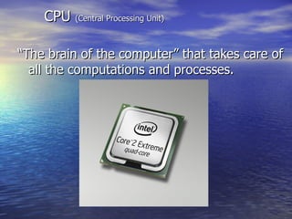


The CPU, or central processing unit, is the brain of the computer that performs all computations and processes data. It consists of several main parts including the control unit, which directs operations; the ALU, which performs arithmetic and logical operations; and registers, which temporarily store data and instructions for faster access. The CPU interacts closely with memory (RAM), fetching instructions and data from memory to execute programs.