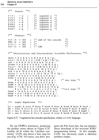
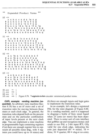
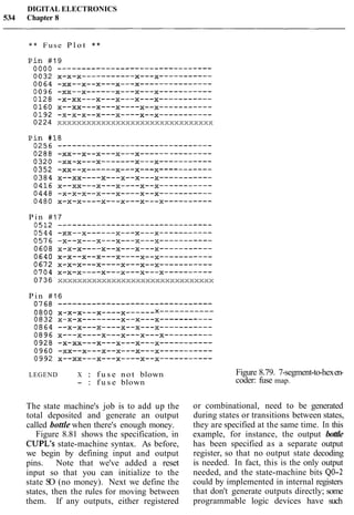
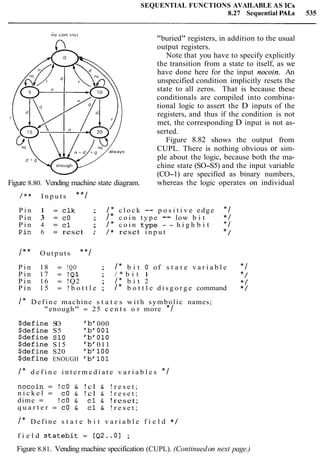
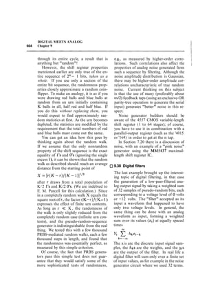
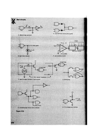
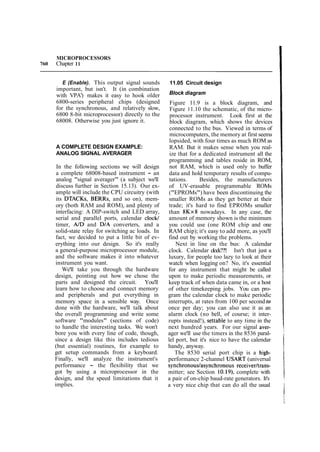
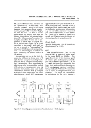
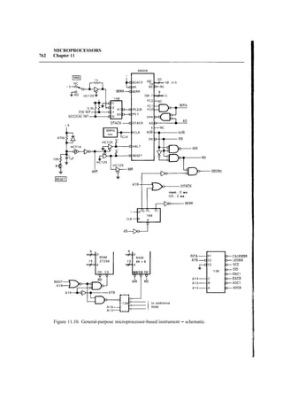
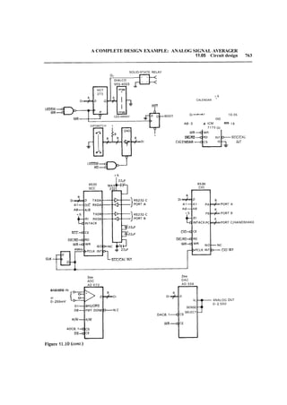
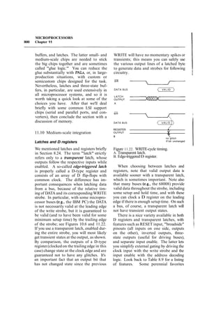
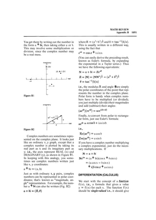
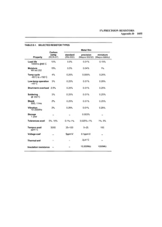
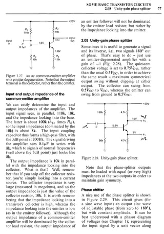
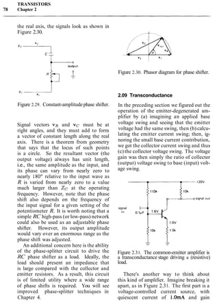
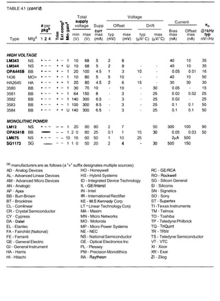
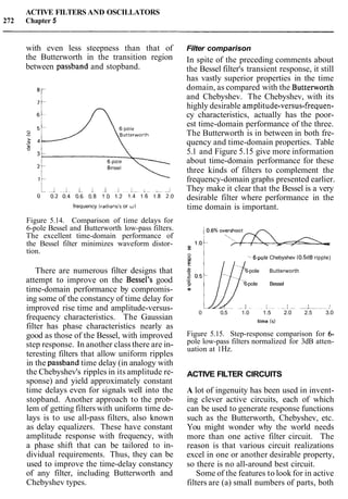
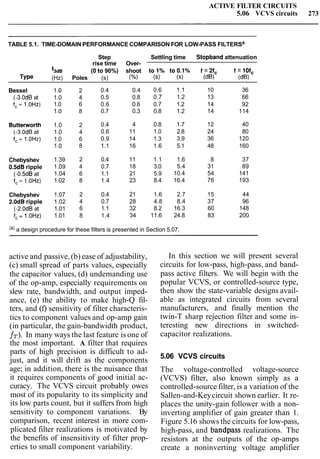
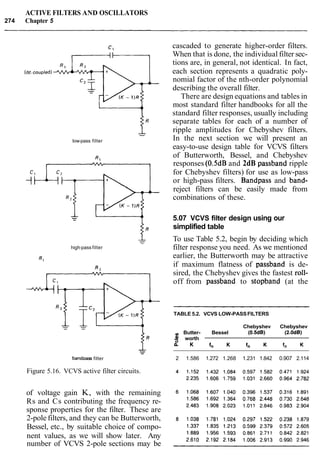
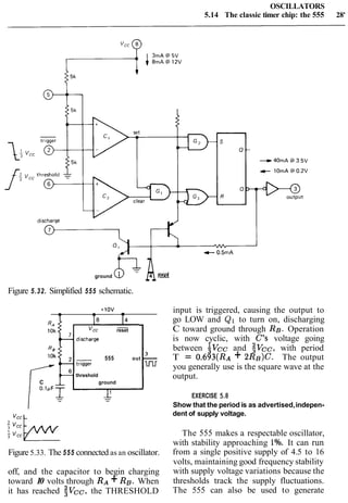
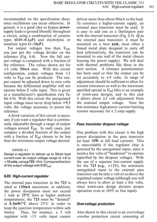
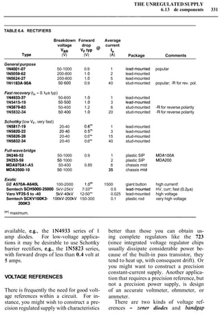
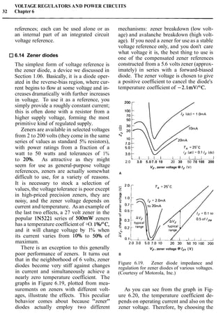
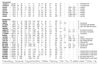
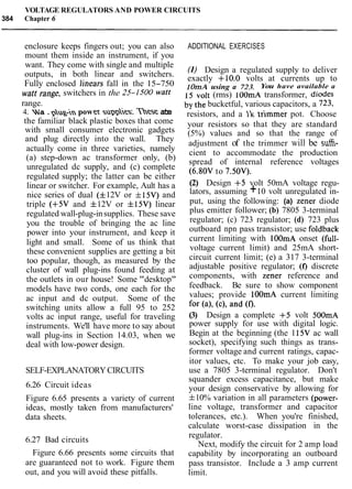
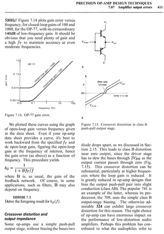
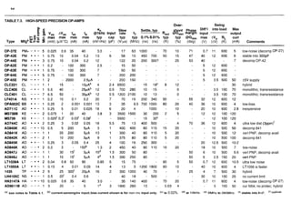
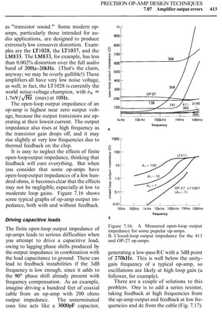
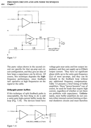
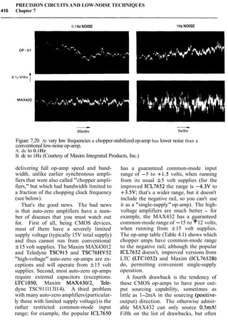
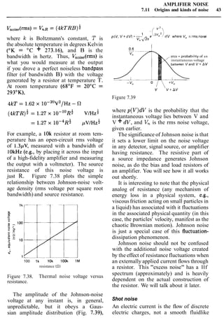
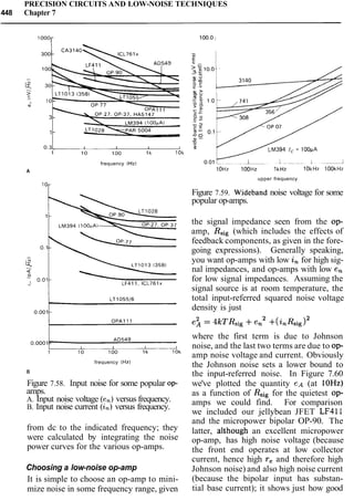
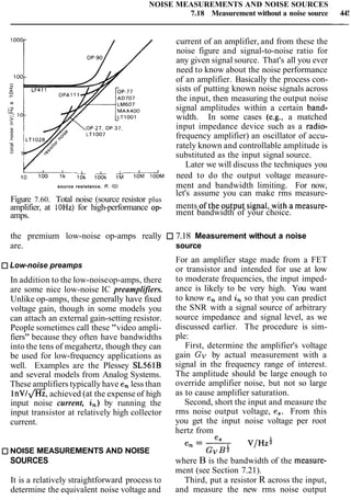
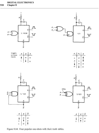
This document provides an overview and table of contents for the book "The Art of Electronics - 2nd Edition" by Paul Horowitz and Winfield Hill. The book covers a wide range of topics in electronics including foundations of voltage, current and resistance, transistors, operational amplifiers, active and digital filters, digital electronics, precision circuits and interfacing between analog and digital domains. It contains 36 chapters and over 1000 pages of content. The table of contents provides a high-level outline of the topics, subtopics and sections covered in each chapter.

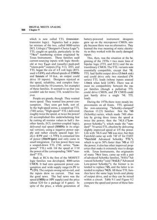
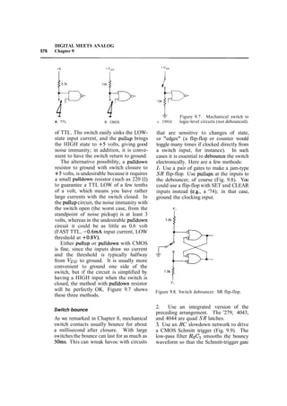
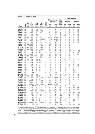
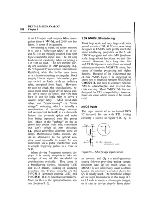
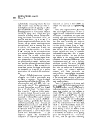
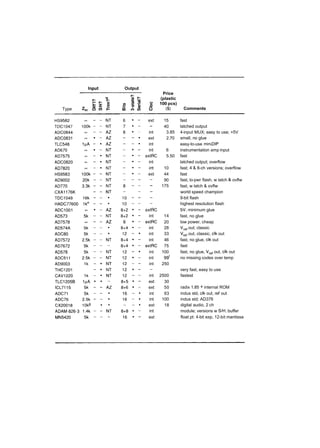
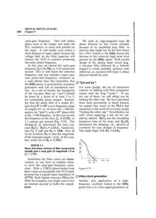
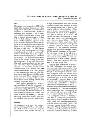
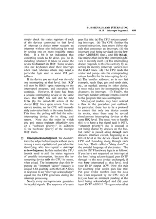
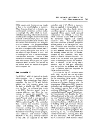
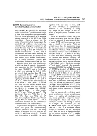
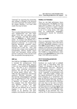
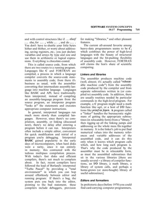
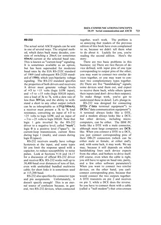
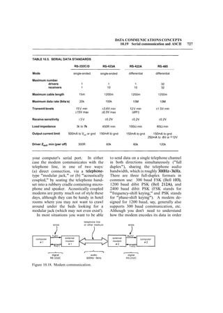
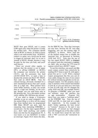
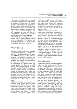
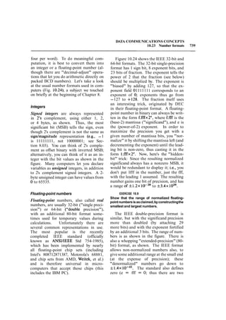
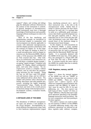
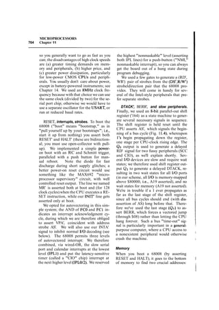
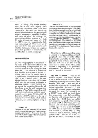
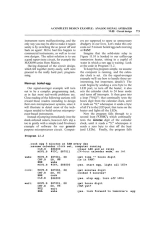
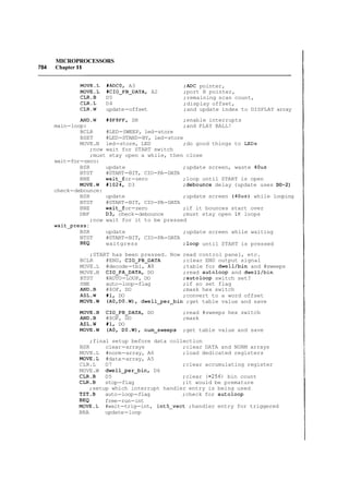
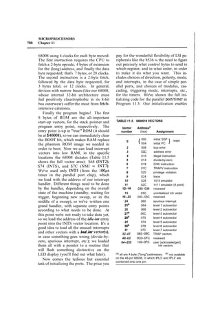
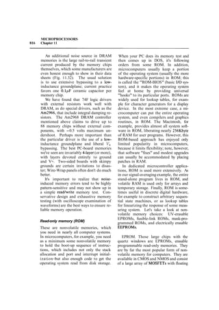
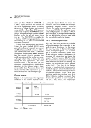
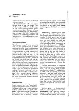
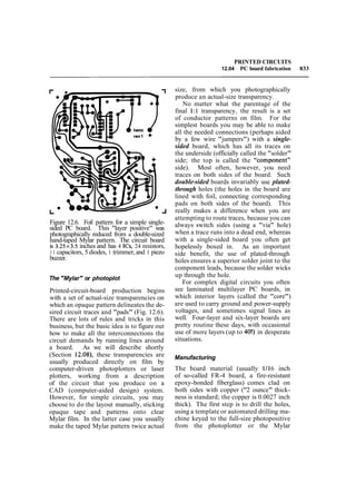
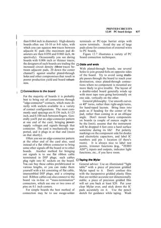
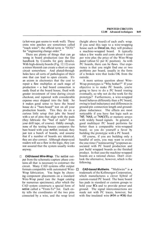
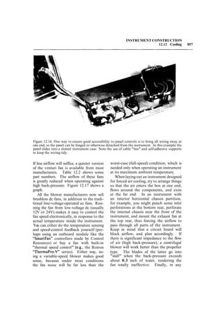
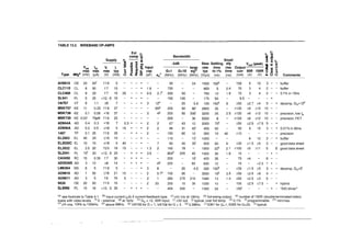
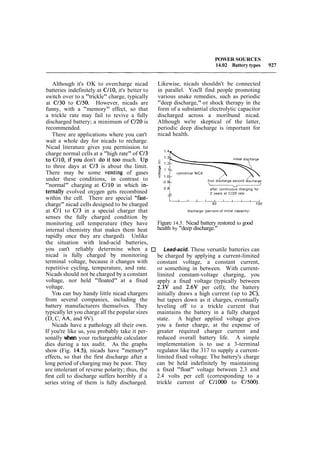
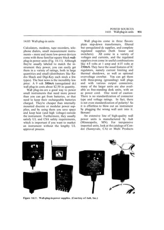
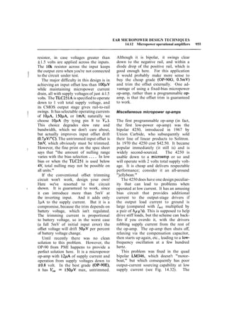
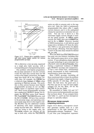
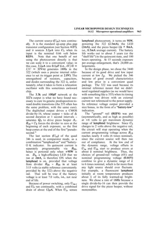
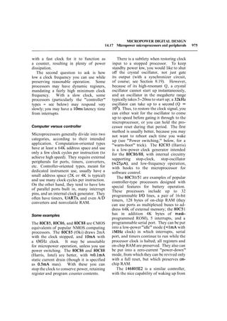
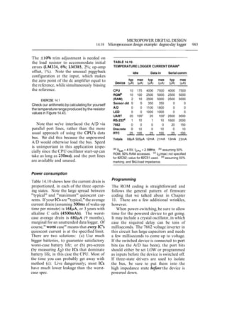
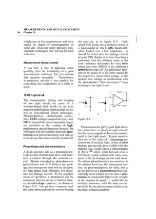
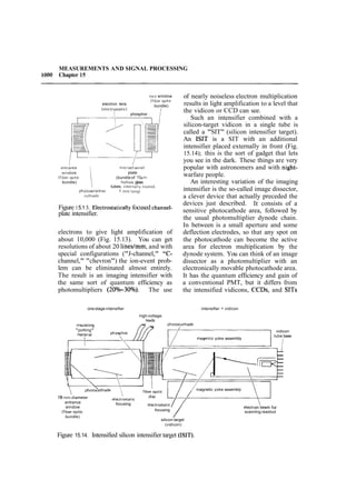
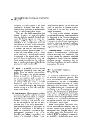
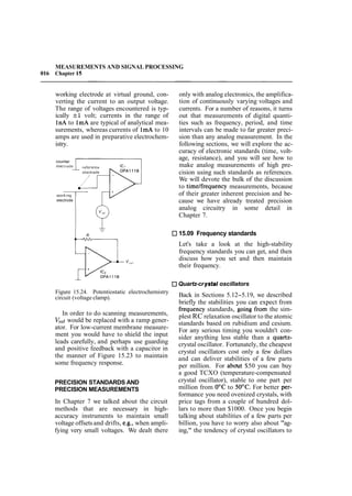
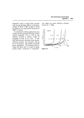
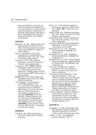
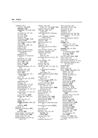
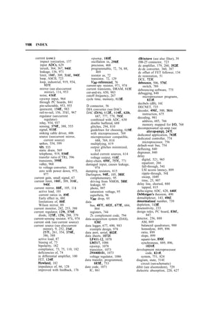
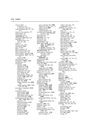
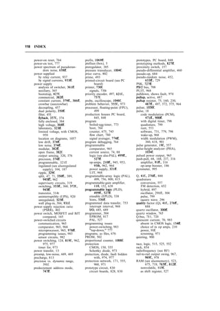
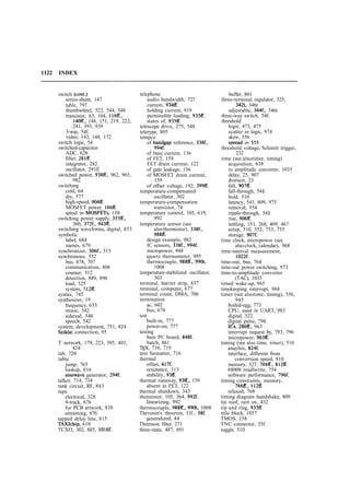
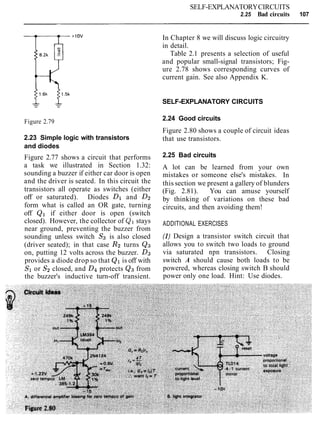
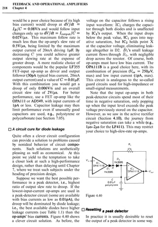
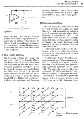
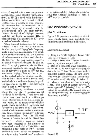
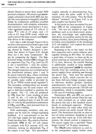
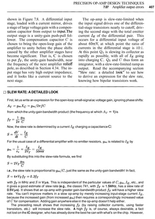
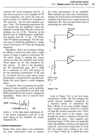
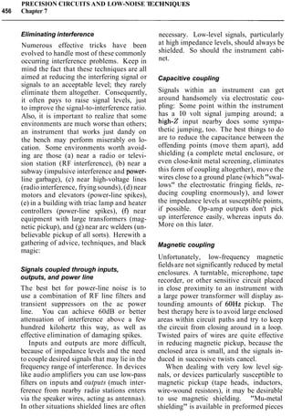
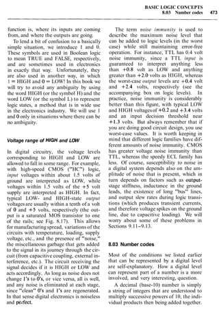
![SOME BASIC TRANSISTOR CIRCUITS
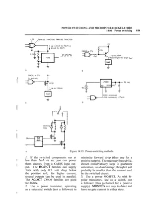
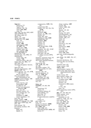
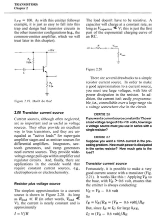
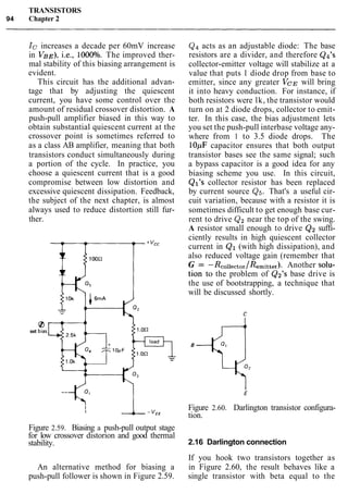
2.06 Transistor current source 73
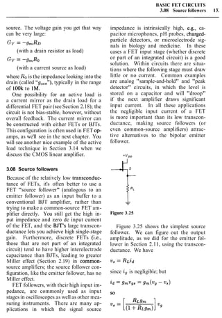
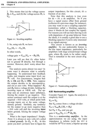
independent of Vc, as long as the transis-
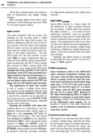
tor is not saturated (Vc > VE+0.2 volt).
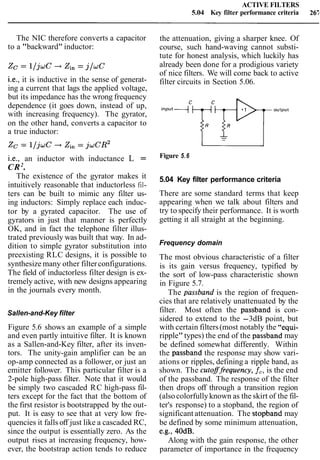
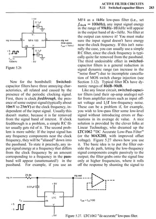
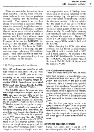
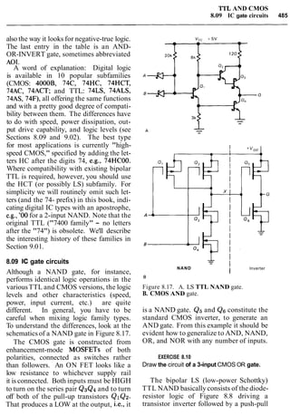
Figure 2.21. Transistor current source: basic
concept.
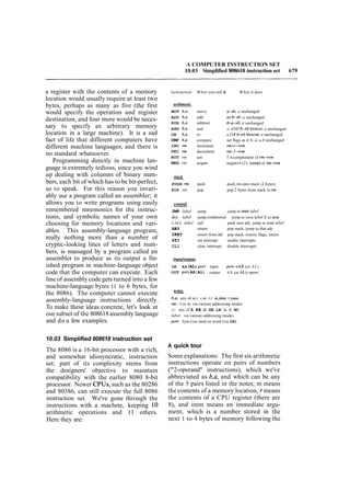
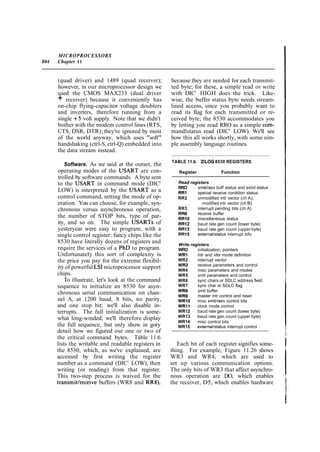
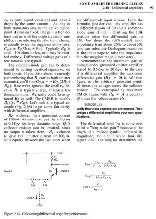
Current-source biasing
The base voltage can be provided in a
number of ways. A voltage divider is
OK, as long as it is stiff enough. As
before, the criterion is that its impedance
should be much less than the dc impedance
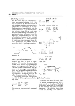
looking into the base (hFERE). Or you
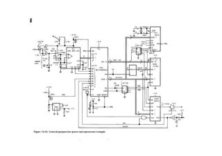
can use a zener diode, biased from Vcc,
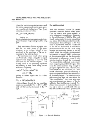
or even a few forward-biased diodes in
series from base to the corresponding
emitter supply. Figure 2.22 shows some
examples. In the last example (Fig. 2.22C),
a pnp transistor sources current to a load
returned to ground. The other examples
(using npn transistors) should properly be
called current sinks, but the usual practice
is to call all of them current sources.
["Sink" and "source" simply refer to the
direction of current flow: If a circuit
supplies (positive) current to a point, it is a
source, and vice versa.] In the first circuit,
the voltage-divider impedance of -1.3k is
very stiff compared with the impedance
looking into the base of about lOOk (for
hFE= loo), SO any changes in beta with
collector voltage will not much affect the
output current by causing the base voltage
to change. In the other two circuits the
biasing resistors are chosen to provide
several milliamps to bring the diodes into
conduction.
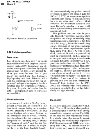
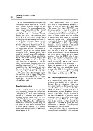
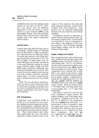
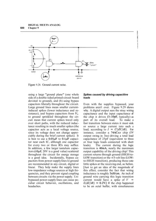
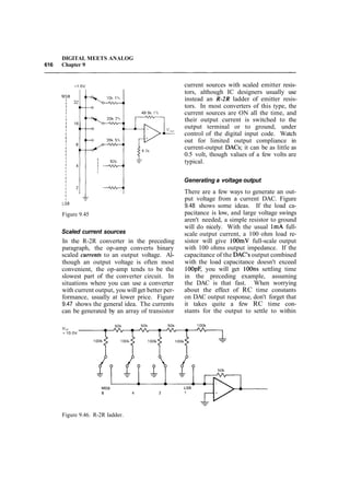
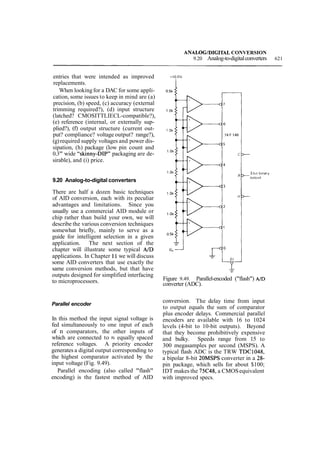
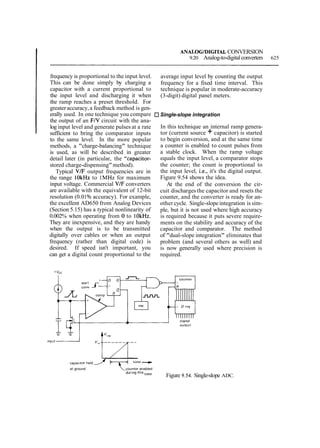
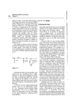
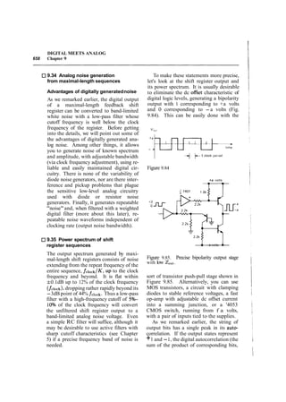
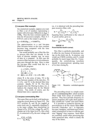
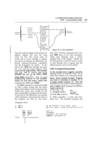
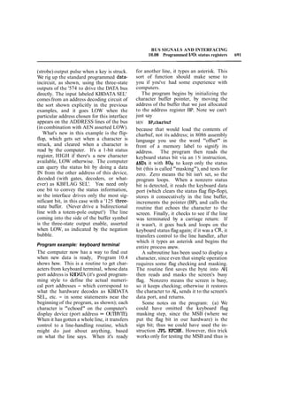
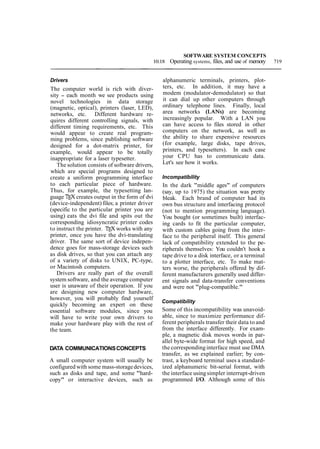
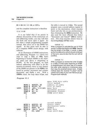
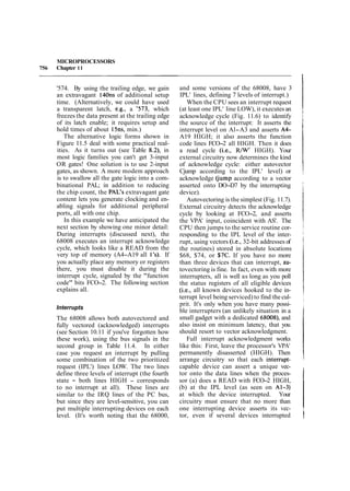
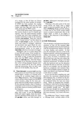
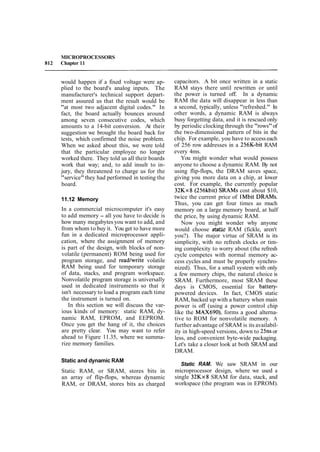
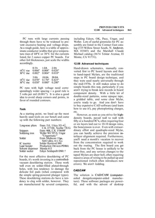
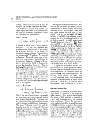
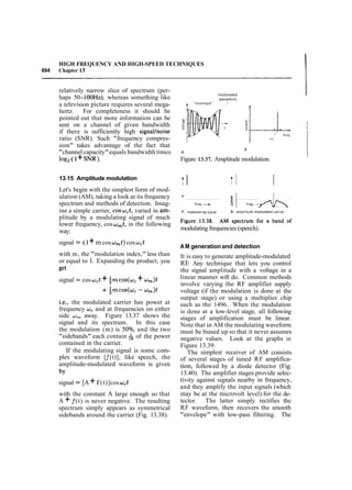
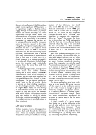
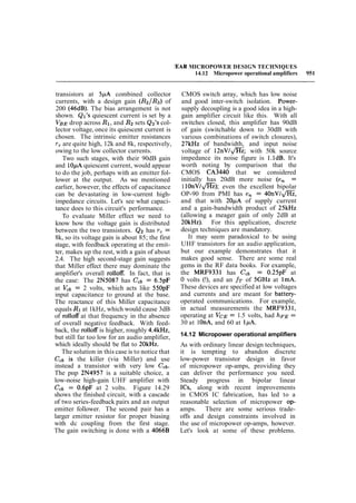
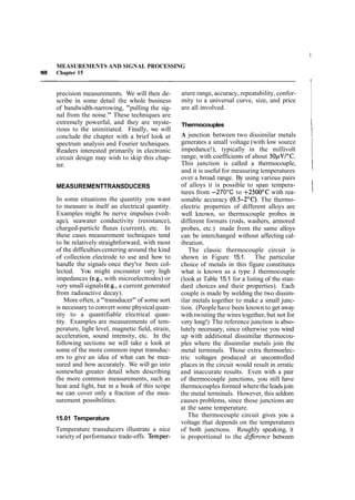
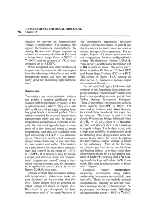
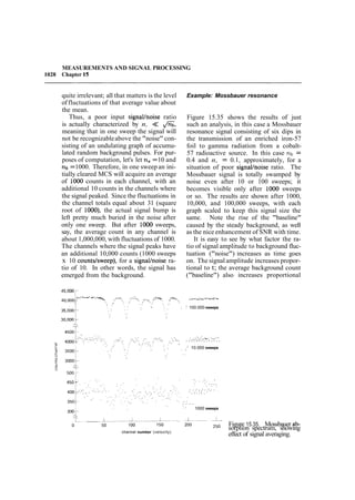
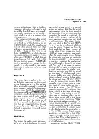
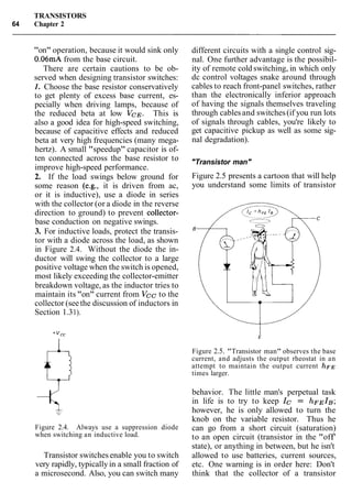
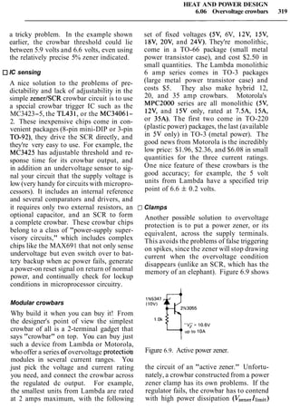
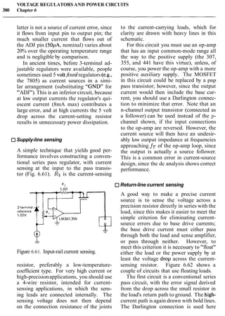
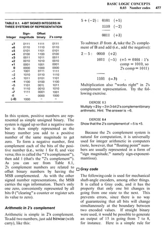
Compliance
A current source can provide constant
current to the load only over some finite
range of load voltage. To do otherwise
would be equivalent to providing infinite
power. The output voltage range over
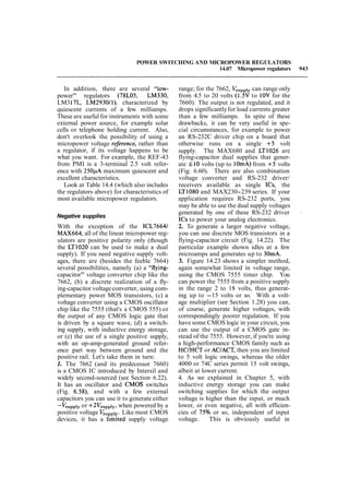
which a current source behaves well is
called its output compliance. For the
preceding transistor current sources, the
compliance is set by the requirement that
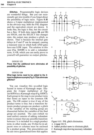
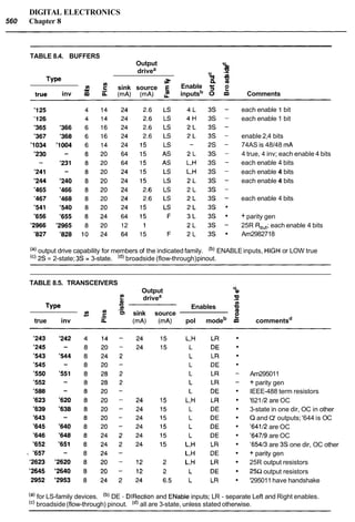
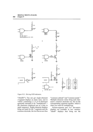
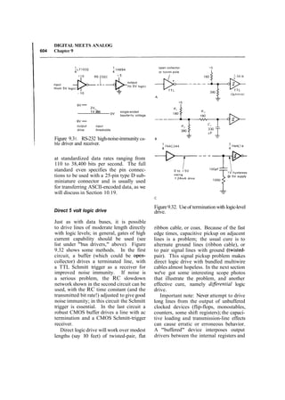
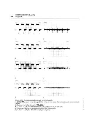
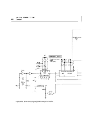
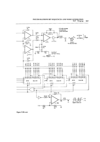
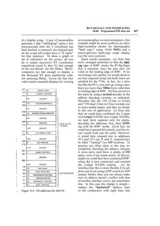
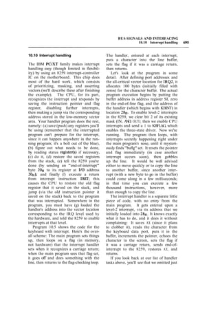
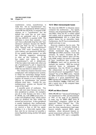
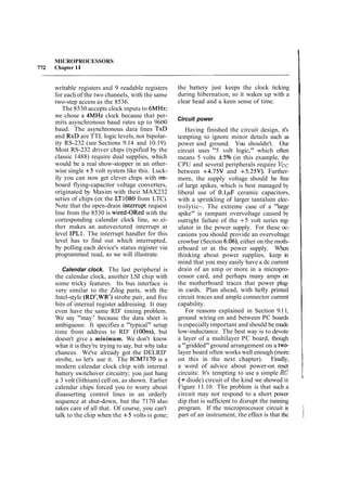
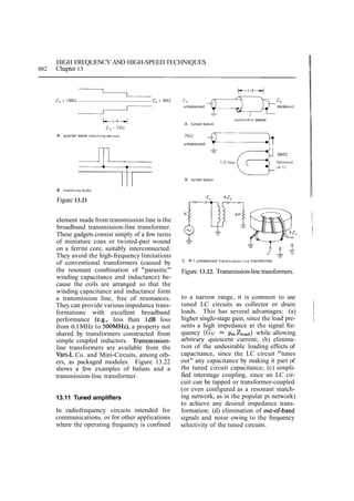
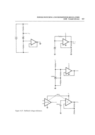
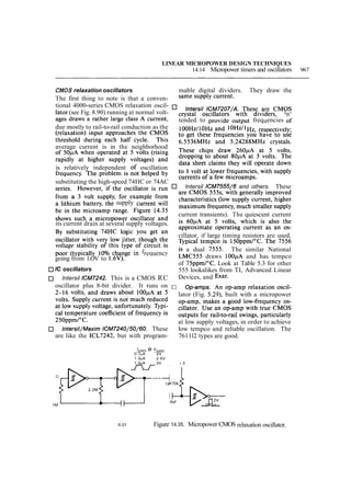
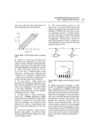
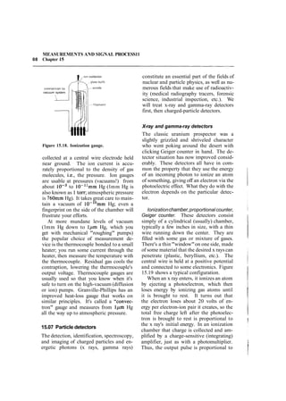
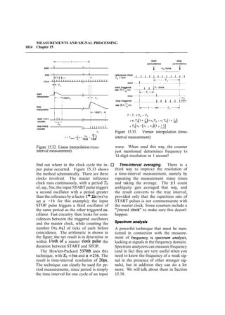
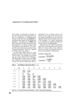
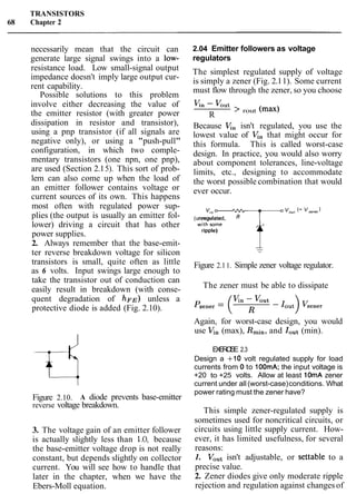
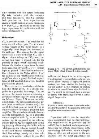
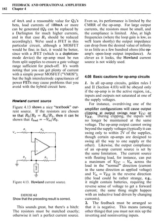
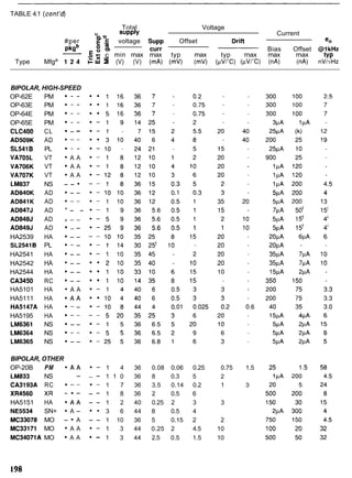
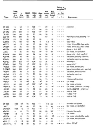
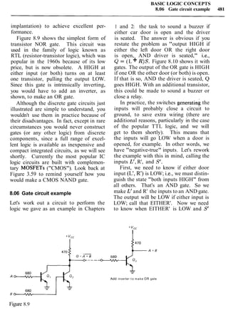
Figure 2.22. Transistor-current-source circuits, illustrating three methods of base biasing; npn
transistors sink current, whereas pnp transistors source current. The circuit in C illustrates a load
returned to ground.](https://image.slidesharecdn.com/theartofelectronics-130527061117-phpapp01/85/The-art-of_electronics-26-320.jpg?cb=1674599069)
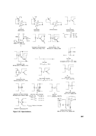
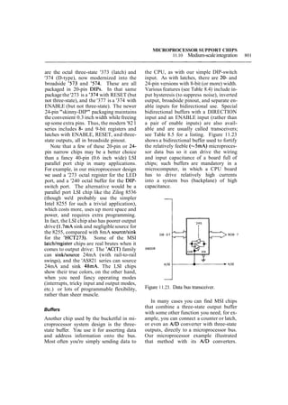
![EBERS-MOLL MODEL APPLIED TO BASIC TRANSISTOR CIRCUITS
2.11 The emitter follower revisited 81
several important quantities we will be
using often in circuit design:
1. The steepness of the diode curve. How
much do we need to increase VBE to in-
crease Ic by a factor of lo? From the
Ebers-Moll equation, that's just VT log, 10,
or 60mV at room temperature. Base volt-
age increases 60rnV per decade of collector
current. Equivalently, Ic = ~ ~ ~ e ~ ~ / ~ ~ ,
where AV is in millivolts.
2. The small-signal impedance looking
into the emitter, for the base held at a fixed
voltage. Taking the derivative of VBE with
respect to Ic, you get
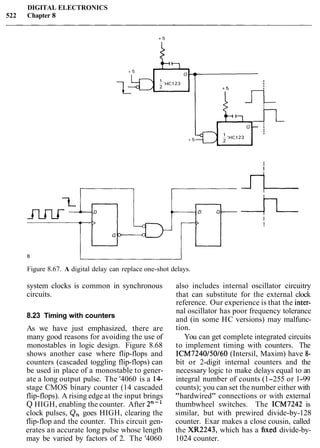
re = VT/IC = 25/Ic ohms
where Ic is in milliamps. The numerical
value 25/Ic is for room temperature. This
intrinsic emitter resistance, re,acts as if it
is in series with the emitter in all transistor
circuits. It limits the gain of a grounded
emitter amplifier, causes an emitter fol-
lower to have a voltage gain of slightly less
than unity, and prevents the output imped-
ance of an emitter follower from reaching
zero. Note that the transconductance of a
grounded emitter amplifier is g, = l/re.
3. The temperature dependence of VBE.
A glance at the Ebers-Moll equation sug-
gests that VBE has a positive temperature
coefficient. However, because of the tem-
perature dependence of Is, VBE decreases
about 2.1mV/OC. It is roughly proportional
to l/T,b,, where Tabsis the absolute tem-
perature.
There is one additional quantity we
will need on occasion, although it is not
derivable from the Ebers-Moll equation. It
is the Early effect we described in Section
2.06, and it sets important limits on
current-source and amplifier performance,
for example:
4. Early effect. VBE varies slightly with
changing VCE at constant Ic. This effect
is caused by changing effective base width,
and it is given, approximately, by
where cr =0.0001.
These are the essential quantities we
need. With them we will be able to handle
most problems of transistor circuit design,
and we will have little need to refer to the
Ebers-Moll equation itself.
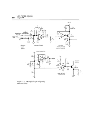
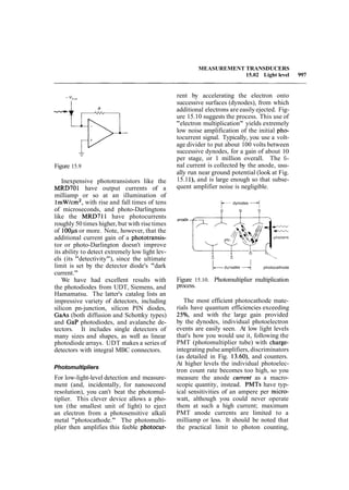
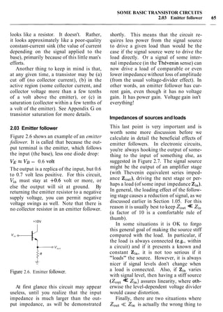
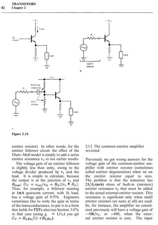
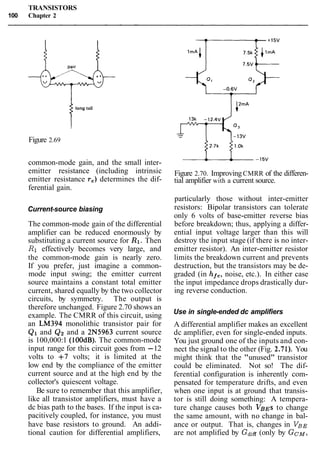
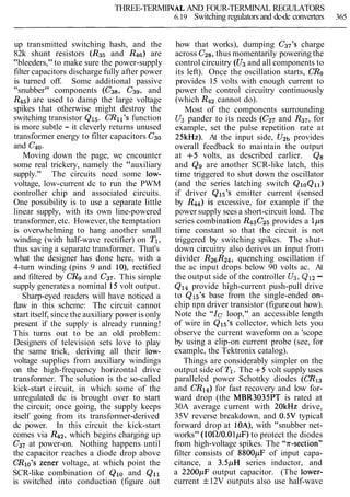
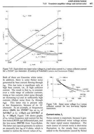
2.11 The emitter follower revisited
Before looking again at the common-emit-
ter amplifier with the benefit of our new
transistor model, let's take a quick look
at the humble emitter follower. The
Ebers-Moll model predicts that an emit-
ter follower should have nonzero out-
put impedance, even when driven by a
voltage source, because of finite re
(item 2, above). The same effect also
produces a voltage gain slightly less
than unity, because re forms a voltage di-
vider with the load resistor.
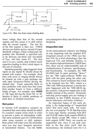
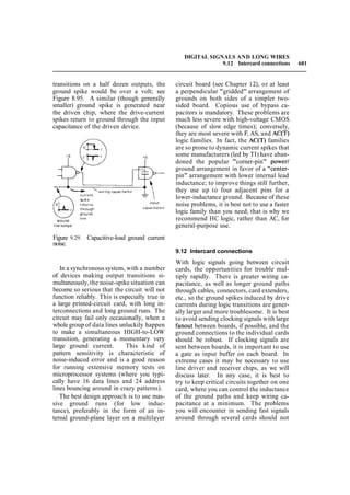
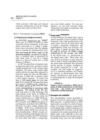
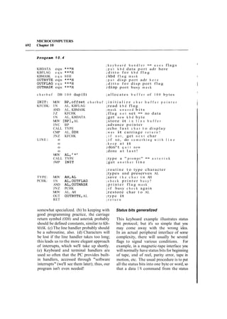
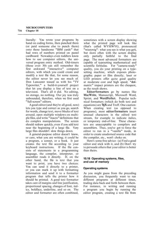
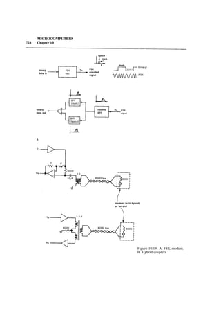
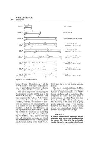
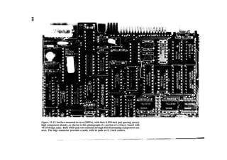
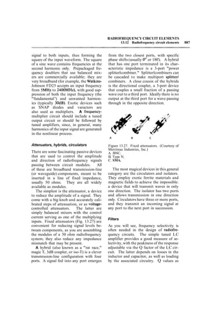
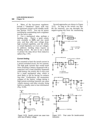
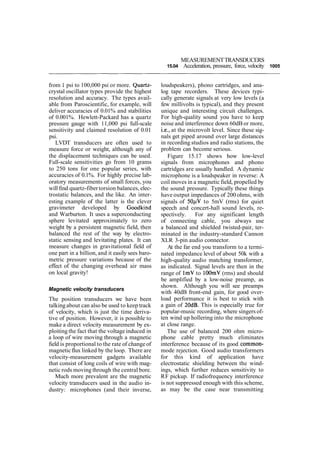
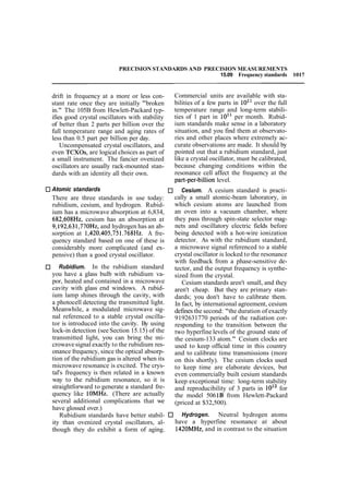
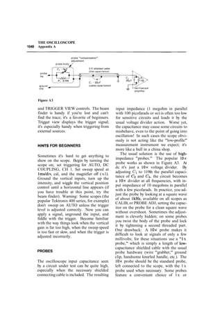
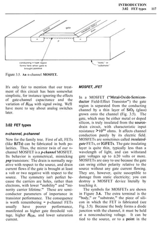
These effectsare easy to calculate. With
fixed base voltage, the impedance look-
ing back into the emitter is just Rout =
d v ~ , q / d I ~ ;but IE M IC, SO Rout X
re, the intrinsic emitter resistance [re =
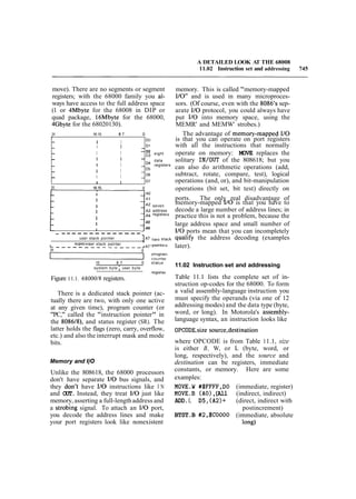
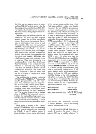
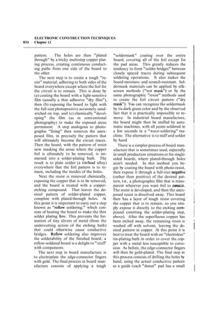
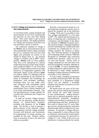
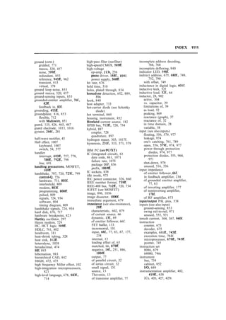
251Ic(mA)]. For example, in Figure
2.34A, the load sees a driving impedance
of re = 25 ohms, since Ic = 1mA. (This
is paralleled by the emitter resistor RE,
if used; but in practice RE will always
be much larger than re.) Figure 2.34B
shows a more typical situation, with finite
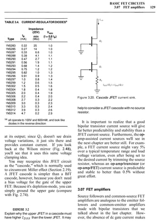
source resistance Rs (for simplicity we've
omitted the obligatory biasing components
- base divider and blocking capacitor -
which are shown in Fig. 2.34C). In this
case the emitter follower's output imped-
ance is just re in series with R,/(hfe+ 1)
(again paralleled by an unimportant RE,
if present). For example, if R, = lk and
Ic = lmA, Rout = 35 ohms (assuming
hf = 100). It is easy to show that the in-
trinsic emitter re also figures into an emit-
ter follower's input impedance, just as if
it were in series with the load (actually, par-
allel combination of load resistor and](https://image.slidesharecdn.com/theartofelectronics-130527061117-phpapp01/85/The-art-of_electronics-34-320.jpg?cb=1674599069)
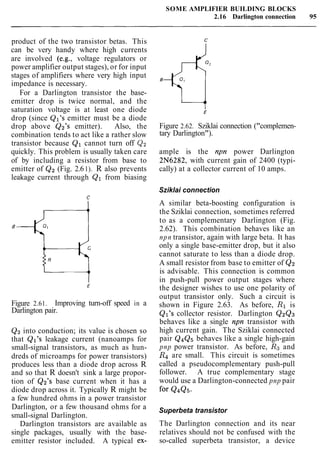
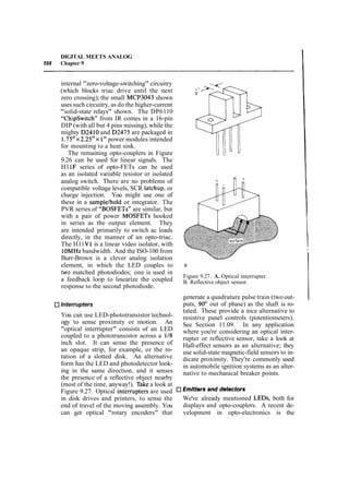
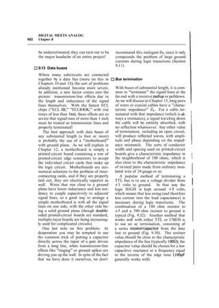
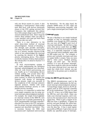
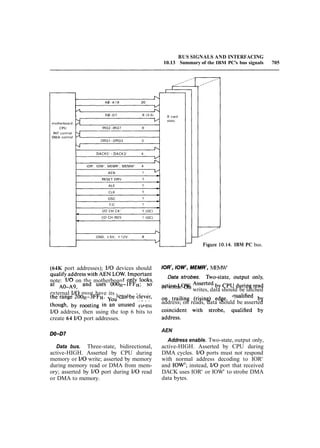
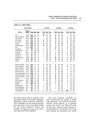
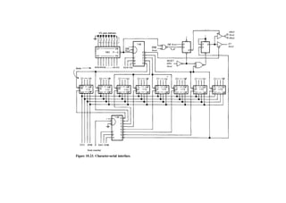
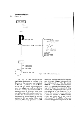
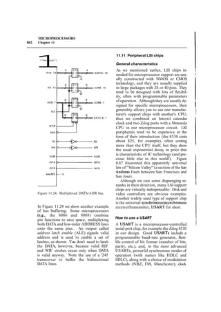
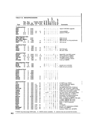
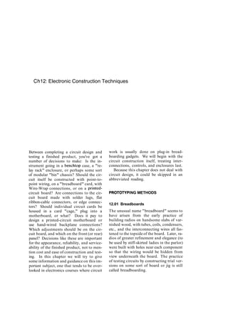
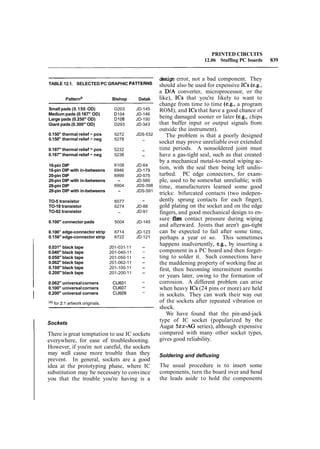
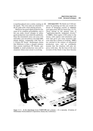
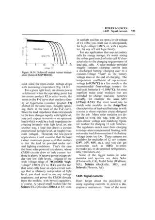
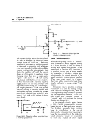
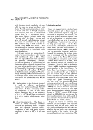
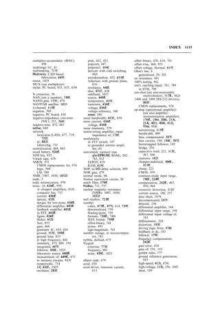
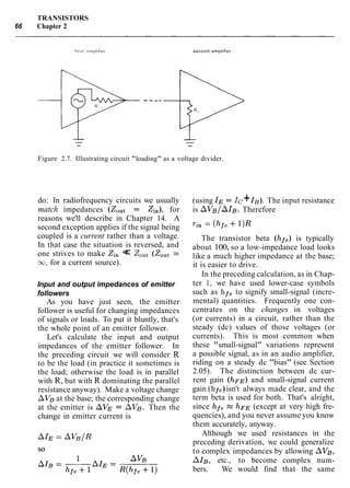
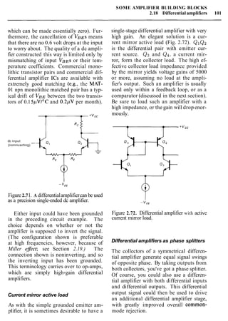
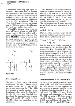
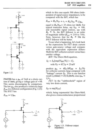
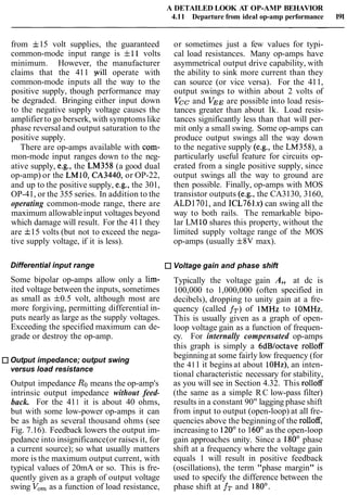
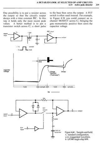
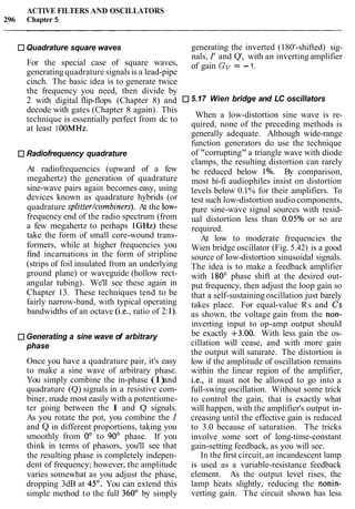
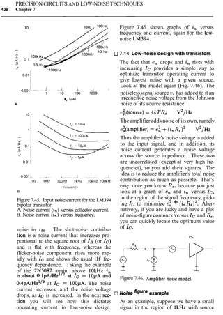
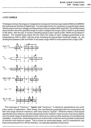
![SOME AMPLIFIER BUILDING BLOCKS
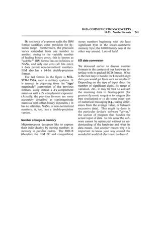
2.17 Bootstrapping 97
this case approximately 100k). But now
the signal-frequency input impedance is
no longer the same as the dc impedance.
Look at it this way: An input wiggle vi,
results in an emitter wiggle VE = vi,. So
the change in current through bias resistor
R3 is 2 = (vin - ~,q)/R3z 0, i.e., Zi,
(due to bias string) = vi,/ii, z infinity.
We've made the loading (shunt) impedance
of the bias network very large at signal
frequencies.
In practice the value of Rg is effectively
increased by a hundred or so, and the
input impedance is then dominated by the
transistor's base impedance. The emitter-
degenerated amplifier can be bootstrapped
in the same way, since the signal on
the emitter follows the base. Note that
the bias divider circuit is driven by the
low-impedance emitter output at signal
frequencies, thus isolating the input signal
from this usual task.
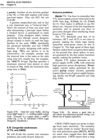
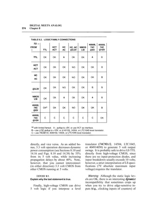
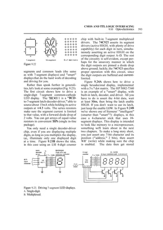
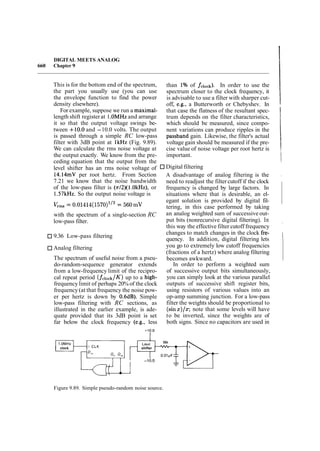
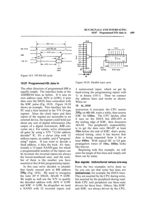
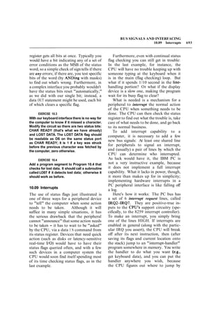
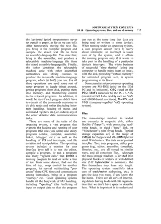
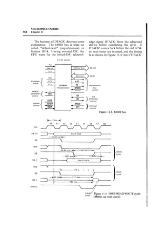
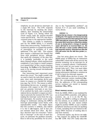
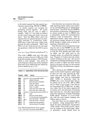
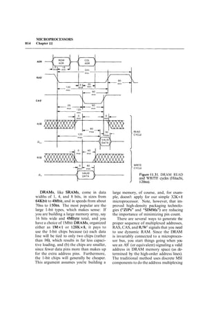
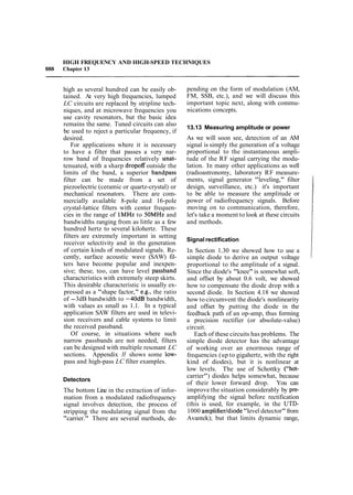
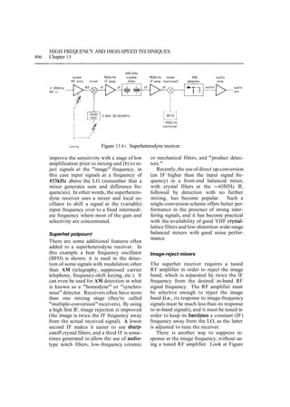
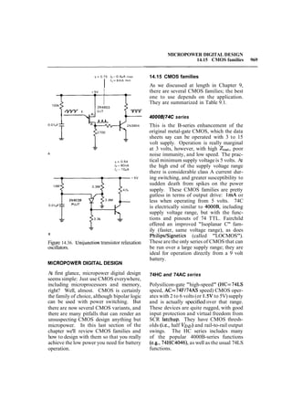
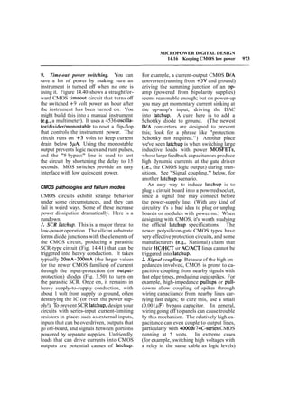
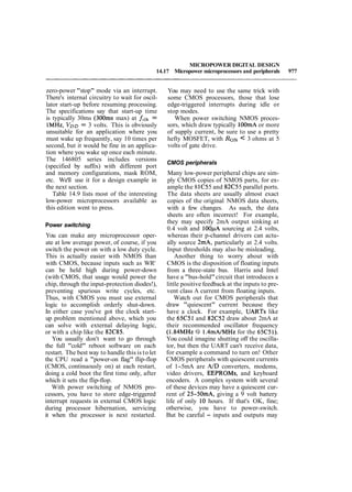
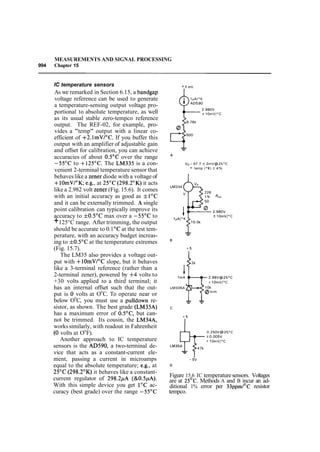
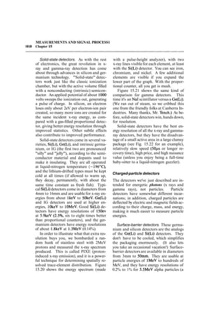
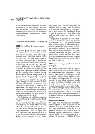
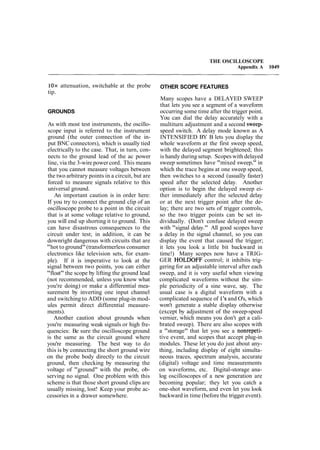
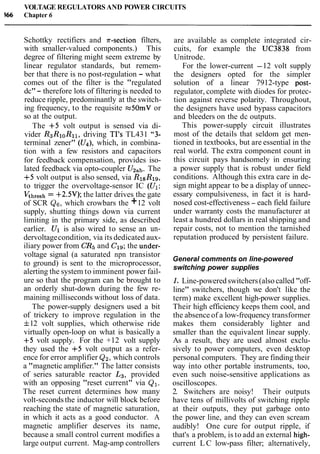
Figure 2.65. Raising the input impedance of
an emitter follower at signal frequencies by
bootstrapping the base bias divider.
Another way of seeing this is to notice
that R3 always has the same voltage across
it at signal frequencies (since both ends
of the resistor have the same voltage
changes), i.e., it's a current source. But
a current source has infinite impedance.
Actually, the effective impedance is less
than infinity because the gain of a follower
is slightly less than 1. That is so because
the base-emitter drop depends on collector
current, which changes with the signal
level. You could have predicted the same
result from the voltage-dividing effect of
the impedance looking into the emitter
[re = 25/Ic(mA) ohms] combined with
the emitter resistor. If the follower has
voltage gain A ( A z 1)' the effective value
of R3 at signal frequencies is
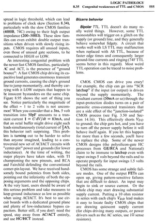
Figure 2.66. Bootstrapping driver-stage collec-
tor load resistor in a power amplifier.
Bootstrapping collector load resistors
The bootstrap principle can be used to in-
crease the effective value of a transistor's
collector load resistor, if that stage drives
a follower. That can increase the voltage
gain of the stage substantially [recall that
Gv = -gmRc, with g, = 1/(RE+re)].
Figure 2.66 shows an example of a boot-
strapped push-pull output stage similar to
the push-pull follower circuit we saw ear-
lier. Because the output follows Qn's base](https://image.slidesharecdn.com/theartofelectronics-130527061117-phpapp01/85/The-art-of_electronics-50-320.jpg?cb=1674599069)
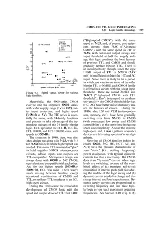
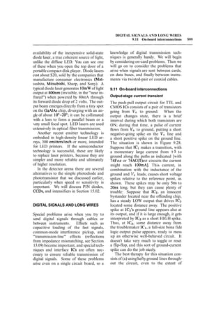
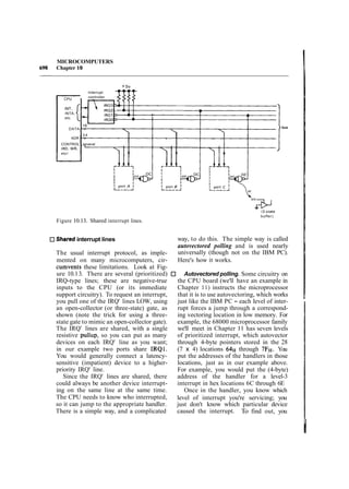
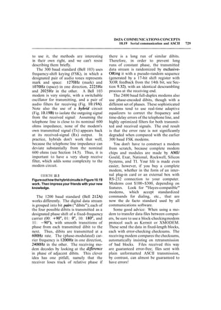
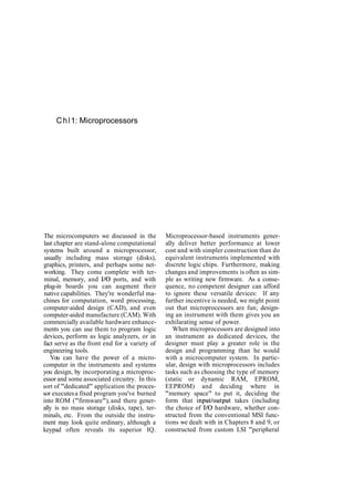
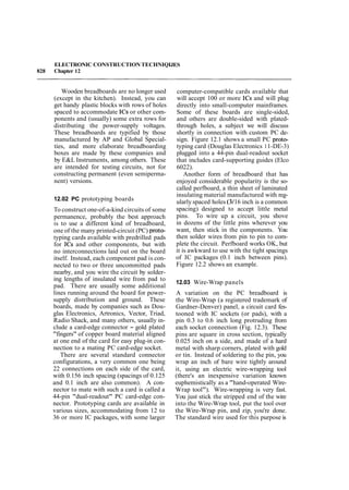
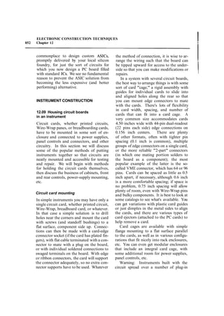
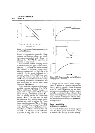
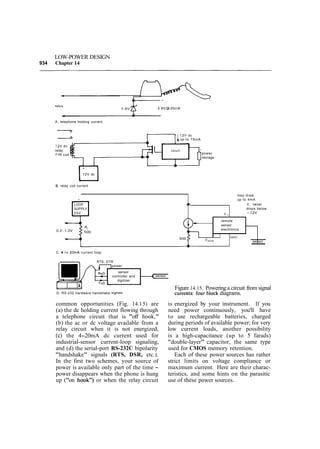
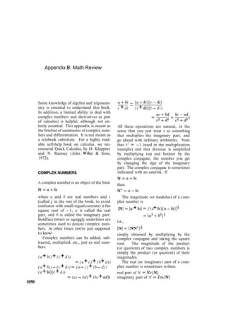
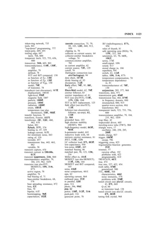
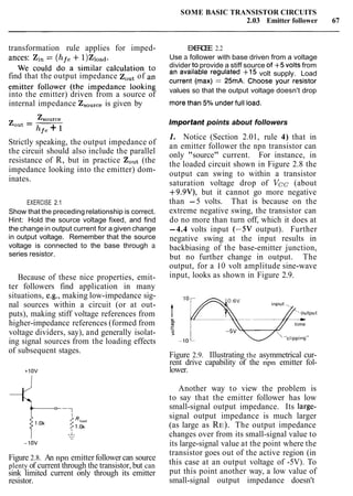
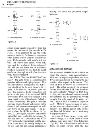
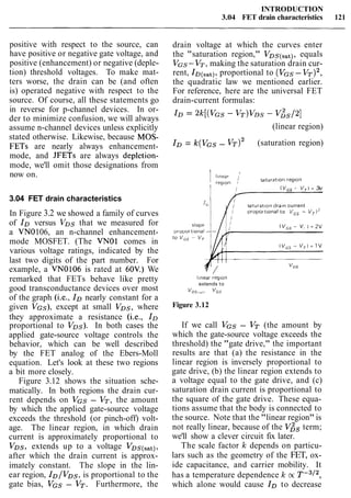
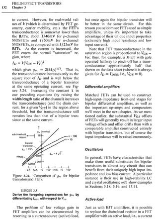
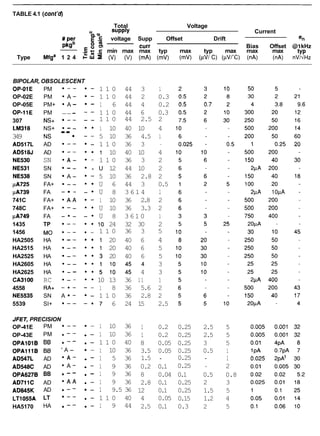
![FIELD-EFFECT TRANSISTORS
114 Chapter 3
First, though, some motivation and per-
spective: The FET's nonexistent gate cur-
rent is its most important characteristic.
The resulting high input impedance (which
can be greater than 1 0 ~ ~ 0 )is essential in
many applications, and in any case it
makes circuit design simple and fun. For
applications like analog switches and am-
plifiersof ultrahigh input impedance, FETs
have no equal. They can be easily used by
themselves or combined with bipolar tran-
sistors to make integrated circuits: In the
next chapter we'll see how successful that
process has been in making nearly perfect
(and wonderfully easy to use) operational
ampl$ers, and in Chapters 8-11 we'll see
how digital electronics has been revolu-
tionized by MOSFET integrated circuits.
Because many FETs using very low current
can be constructed in a small area, they
are especially useful for large-scale integra-
tion (LSI) digital circuits such as calculator
chips, microprocessors, and memories. In
addition, high-current MOSFETs (30A or
more) of recent design have been replacing
bipolar transistors in many applications,
often providing simpler circuits with im-
proved performance.
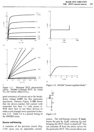
3.01 FET characteristics
Beginners sometimes become catatonic
when directly confronted with the confus-
ing variety of FET types (see, for exam-
ple, the first edition of this book!), a vari-
ety that arises from the combined choices
of polarity (n-channel or p-channel), form
of gate insulation (semiconductor junction
[JFET]or oxide insulator[MOSFET]), and
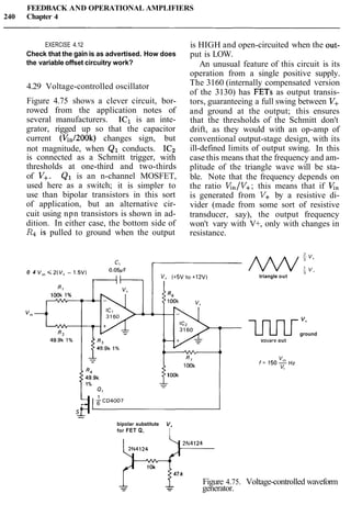
channel doping (enhancement or depletion
mode). Of the eight resulting possibilities,
six could be made, and five actually are.
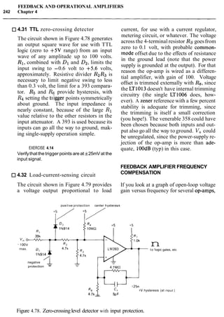
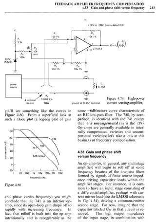
Four of those five are of major importance.
It will aid understanding (and sanity),
however, if we begin with one type only,
just as we did with the npn bipolar tran-
sistor. Once comfortable with FETs, we'll
have little trouble with their family tree.
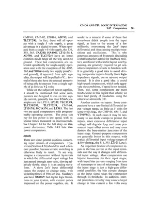
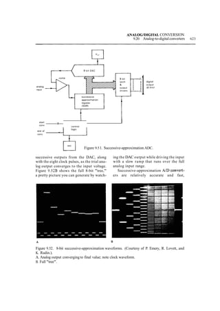
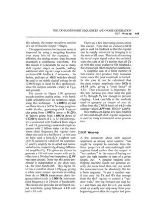
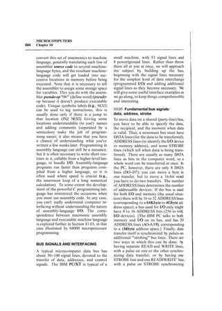
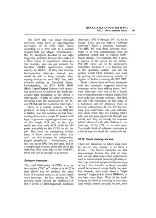
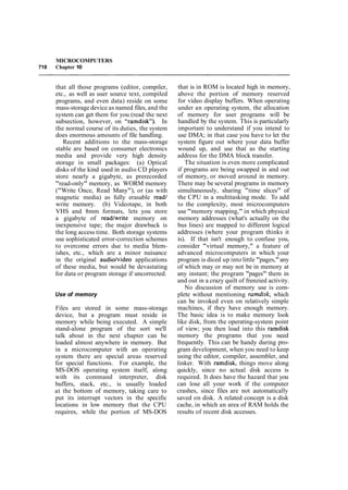
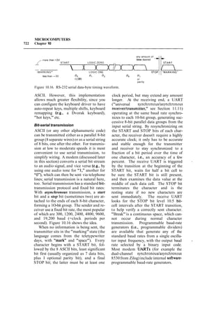
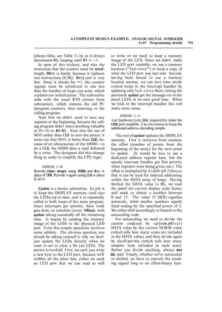
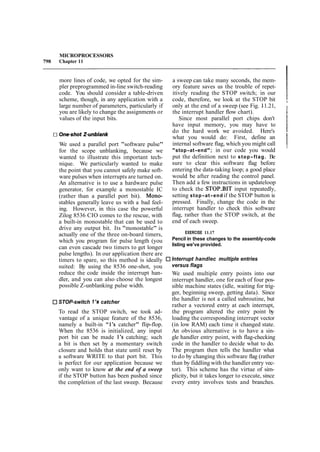
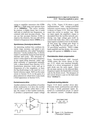
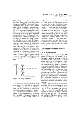
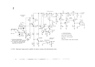
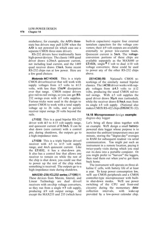
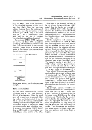
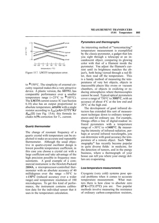
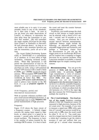
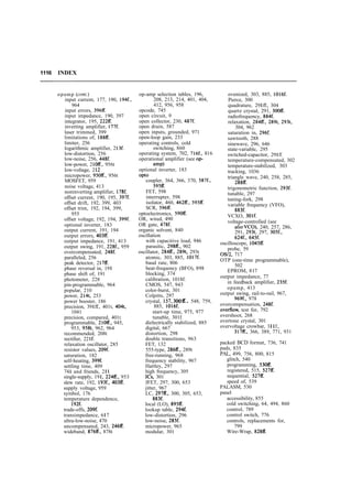
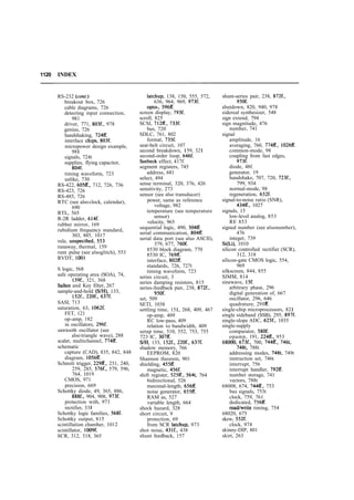
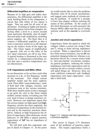
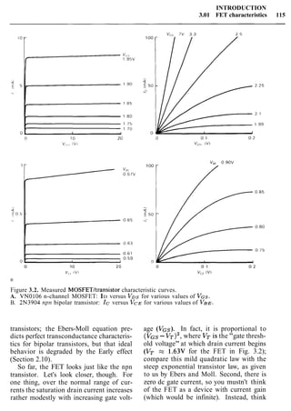
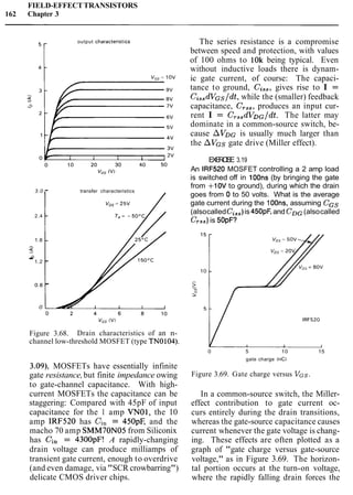
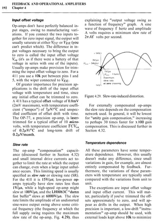
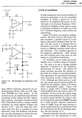
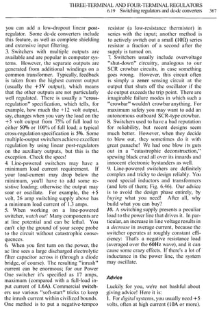
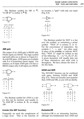
FET V-l curves
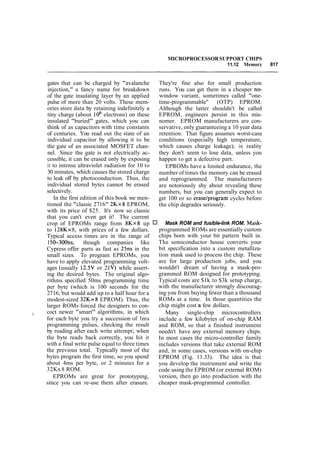
Let's look first at the n-channel enhance-
ment-mode MOSFET, which is analogous
to the npn bipolar transistor (Fig. 3.1). In
normal operation the drain collector) is
more positive than the source (-emitter).
No current flows from drain to source
unless the gate base) is brought positive
with respect to the source. Once the
gate is thus "fonvard-biased" there will be
drain current, all of which flows to the
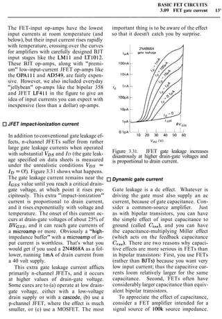
source. Figure 3.2 shows how the drain
current IDvaries with drain-source voltage
VDs, for a few values of controlling gate-
source voltage VGS.For comparison, the
corresponding "family" of curves of Ic
versus VBEfor an ordinary npn bipolar
transistor is shown. Obviously threre are
a lot of similarities between n-channel
MOSFETs and npn bipolar transistors.
d r a ~ n collector
source emitter
n~channelMOSFET npn b~polartransistor
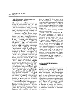
Figure 3.1
Like the npn transistor, the FET has a
high incremental drain impedance, giving
roughly constant current for VDs greater
than a volt or two. By an unfortunate
choice of language, this is called the "satu-
ration" region of the FET and corresponds
to the "active" region of the bipolar tran-
sistor. Analogous to the bipolar transistor,
larger gate-to-source bias produces larger
drain current. If anything, FETs behave
more nearly like ideal transconductance
devices (constant drain current for con-
stant gate-source voltage) than do bipolar](https://image.slidesharecdn.com/theartofelectronics-130527061117-phpapp01/85/The-art-of_electronics-66-320.jpg?cb=1674599069)
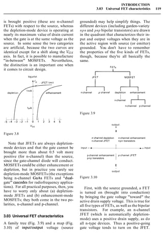
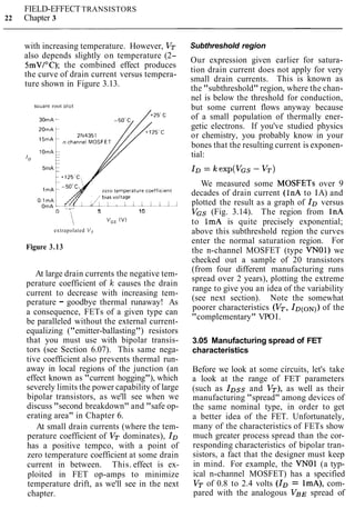
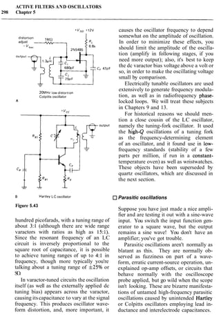
![FIELD-EFFECT TRANSISTORS
140 Chapter 3
Figure 3.33. Variable-gain circuits.
-
ac (signal) gain. Without the capacitor,
the transistor biasing would vary with FET
resistance.
out
EXERCISE 3.7
The VN13 has an ON resistance (VGS= +5V)
of 15 ohms(max). Whatis the rangeof amplifier
gain in the second circuit (assume that the
current sink looks like 1MR)? What is the low-
frequency3dB point when the FET is biased so
that the amplifier gain is (a) 40dB or (b) 20dB?
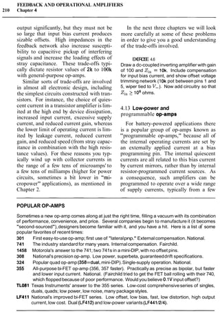
56k
- 125OPA
v4(4:l current
- m~rror)
-
VCO~,,OI VN13
(positive1
The linearization of RDs with a resis-
tive gate divider circuit, as above, is re-
markably effective. In Figure 3.34 we've
compared actual measured curves of ID
versus VDs in the linear (low-VDs) region
for FETs with and without the linearizing
circuit. The linearizing circuit is essential
for low-distortion applications with signal
swings of more than a few millivolts.
When considering FETs for an appli-
cation requiring a gain control, e.g., an
AGC or "modulator" (in which the am-
plitude of a high-frequency signal is var-
ied at an audio rate, say), it is worth-
while to look also at "analog-multiplier"
ICs. These are high-accuracy devices with
good dynamic range that are normally used
to form the product of two voltages. One
of the voltages can be a dc control sig-
nal, setting the multiplication factor of the
device for the other input signal, i.e., the
gain. Analog multipliers exploit the g,-
versus-Ic characteristic of bipolar transis-
tors [g, = Ic(mA)/25 siemens], using
matched arrays to circumvent problems
of offsets and bias shifts. At very high
frequencies (1OOMHz and above), passive
"balanced mixers" (Section 13.12) are of-
ten the best devices to accomplish the same
task.
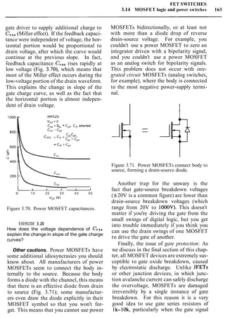
It is important to remember that a
FET in conduction at low VDs behaves
like a good resistance all the way down
to zero volts from drain to source (there
are no diode drops or the like to worry
about). We will see op-amps and digital
logic families (CMOS) that take advantage
of this nice property, giving outputs that
saturate cleanly to the power supplies.
FET SWITCHES
The two examples of FET circuits that
we gave at the beginning of the chapter
were both switches: a logic-switching ap-
plication and a linear signal-switchingcir-
cuit. These are among the most important
FET applications and take advantage of
the FET's unique characteristics: high gate
impedance and bipolarity resistive conduc-
tion clear down to zero volts. In practice](https://image.slidesharecdn.com/theartofelectronics-130527061117-phpapp01/85/The-art-of_electronics-92-320.jpg?cb=1674599069)
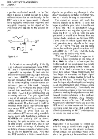

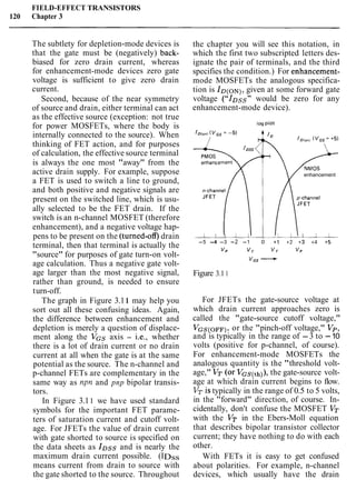
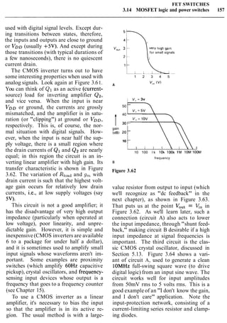
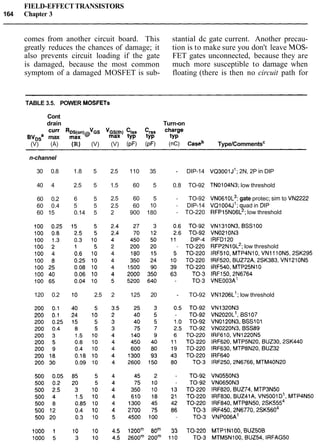
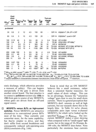
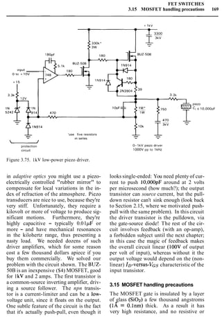
![FET SWITCHES
3.12 Limitations of FET switches 149
signal levelof zero voltsand an output load
consisting of 10k in parallel with 20pC re-
alistic values for an analog switch circuit.
The handsome transients are caused by
charge transferred to the channel, through
the gate-channel capacitance, at the tran-
sitions of the gate. The gate makes a sud-
den step from one supply voltage to the
other, in this case between f15 volt sup-
plies, transferring a slug of charge
Q = CGc [VG(finish) - VG(start)]
CGC is the gate-channel capacitance,
typically around 5pE Note that the amount
of charge transferred to the channel de-
pends only on the total voltage change at
the gate, not on its rise time. Slowing
down the gate signalgives rise to a smaller-
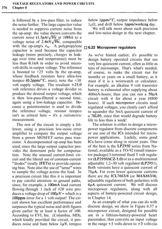
amplitude glitch of longer duration, with
the same total area under its graph. Low-
pass filtering of the switch's output signal
has the same effect. Such measures may
help if the peak amplitude of the glitch
must be kept small, but in general they are
ineffective in eliminating gate feedthrough.
In some cases the gate-channel capacitance
may be predictable enough for you to
cancel the spikes by coupling an inverted
version of the gate signal through a small
adjustable capacitor.
The gate-channel capacitance is distri-
buted over the length of the channel, which
means that some of the charge is coupled
back to the switch's input. As a result, the
size of the output glitch depends on the
signal source impedance and is smallest
when the switch is driven by a voltage
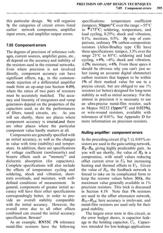
source. Of course, reducing the size of
the load impedance will reduce the size of
the glitch, but this also loads the source
and introduces error and nonlinearity due
to finite RON. Finally, all other things
being equal, a switch with smaller gate-
channel capacitance will introduce smaller
switching transients, although you pay a
price in the form of increased RON.
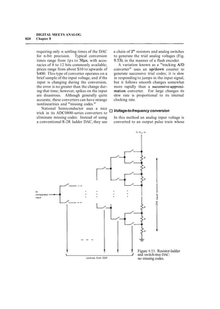
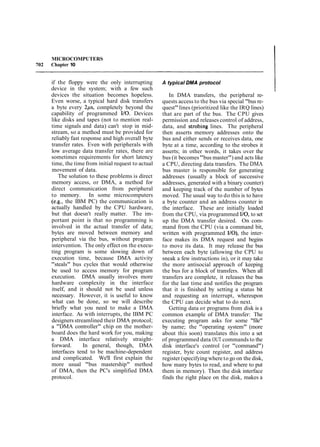
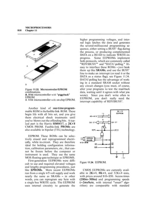
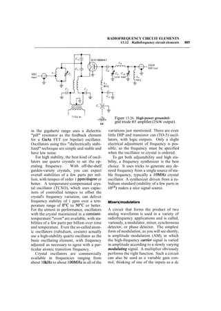
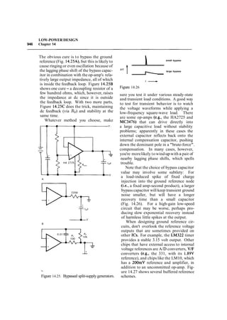
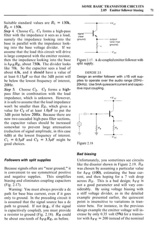
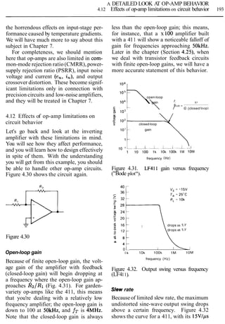
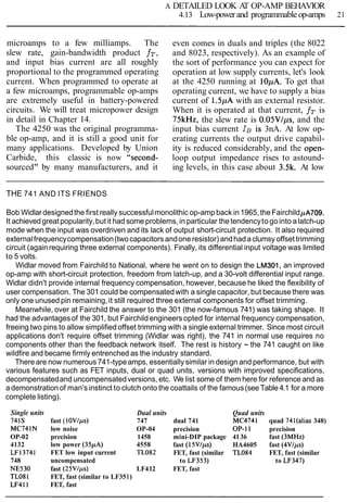
Figure 3.49 shows an interesting com-
parison of gate-induced charge transfers
for three kinds of analog switches, includ-
ing JFETs. In all cases the gate signal
is making a full swing, i.e., either 30
volts or the indicated supply voltage for
MOSFETs, and a swing from -15 volts
to the signal level for the n-channel JFET
switch. The JFET switch shows a strong
Figure 3.49. Charge
transfer for various
, FET linear switches
-15 - 10 - 5 o + 5 + 10 +15 as a function of signal
v,,,,, (V) voltage.](https://image.slidesharecdn.com/theartofelectronics-130527061117-phpapp01/85/The-art-of_electronics-101-320.jpg?cb=1674599069)

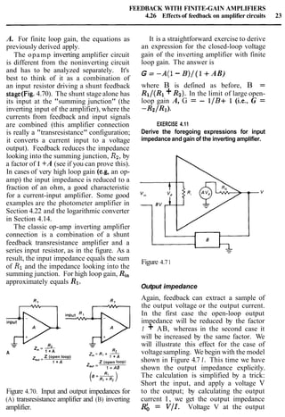
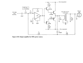
![FEEDBACK WITH FINITE-GAIN AMPLIFIERS
4.26 Effects of feedback on amplifier circuits 23
things so that inputs and outputs can be
currents or voltages.) The input to the gain
block is then V,, - BVout. But the output
is just the input times A:
In other words,
and the closed-loop voltage gain, Vout/Vn,
is just
Some terminology: The standard designa-
tions for these quantities are as follows:
G = closed-loopgain, A = open-loop gain,
AB = loop gain, 1 + AB = return differ-
ence, or desensitivity. The feedback net-
work is sometimes called the beta network
(no relation to transistor beta, hf,).
Figure 4.66
4.26 Effects of feedback on
amplifier circuits
Let's look at the important effects of feed-
back. The most significant are predictabil-
ity of gain (and reduction of distortion),
changed input impedance, and changed
output impedance.
Predictability of gain
The voltage gain is A/(l + AB). In the
limit of infinite open-loop gain A, G =
11B. We saw this result in the noninvert-
ing amplifier configuration, where a volt-
age divider on the output provided the
signal to the inverting input (Fig. 4.69).
The closed-loop voltage gain was just the
inverse of the division ratio of the volt-
age divider. For finite gain A, feedback
still acts to reduce the effects of variations
of A (with frequency, temperature, ampli-
tude, etc.). For instance, suppose A de-
pends on frequency as in Figure 4.67. This
Figure 4.67
will surely satisfy anyone's definition of a
poor amplifier (the gain varies over a fac-
tor of 10 with frequency). Now imagine we
introduce feedback, with B = 0.1 (a sim-
ple voltage divider will do). The closed-
loop voltage gain now varies from 1000/[1
+(1000x0.1)], or 9.90, to 10,000/[1 +
(10,000x0.1)], or 9.99, a variation of just
1% over the same range of frequency! To
put it in audio terms, the original amplifier
is flat to flOdB, whereas the feedback am-
plifier is flat to f0.04dB. We can now re-
cover the original gain of 1000with nearly
this linearity by just cascading three such
stages. It was for just this reason (namely,
the need for extremely flat telephone re-
peater amplifiers) that negative feedback
was invented. As the inventor, Harold
Black, described it in his first open publica-
tion on the invention (Electrical Engineer-
ing, 53:114, 1934),"by building an ampli-
fier whose gain is made deliberately, say
40 decibels higher than necessary (10,000-
fold excess on energy basis) and then feed-
ing the output back to the input in such
a way as to throw away the excess gain, it
has been found possible to effect extraordi-
nary improvement in constancy of ampli-
fication and freedom from nonlinearity."](https://image.slidesharecdn.com/theartofelectronics-130527061117-phpapp01/85/The-art-of_electronics-184-320.jpg?cb=1674599069)
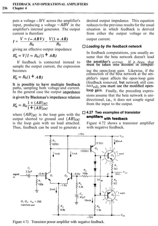
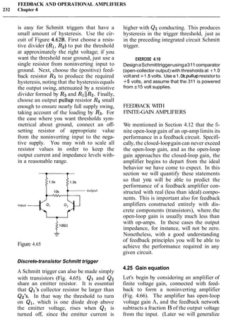
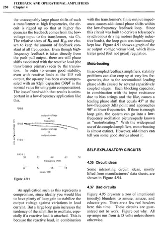
![FEEDBACK WITH FINITE-GAIN AMPLIFIERS
4.27 Two examples of transistor amplifiers with feedback 23'
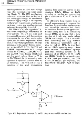
Circuit description important to make sure that the dc re-
It may look complicated, but it is extreme- sistances seen from the inputs are equal,
ly straightforward in design and is rela- as shown (a Darlington input stage would
tively easy to analyze. Q1 and Q2 form probably be better here).
a differential pair, with common-emitter
amplifier Q3 amplifying its output. Rs is Analysis
Q3's collector load resistor, and push-pull analyze this circuit in detail, de-
pair Q4 an' Q5 form the output emitter termining the gain, input and output
follower. The output voltage is sampled by impedances, and distortion. T~ illustrate
the feedback network consisting of voltage the utility of feedback, we will find these
divider R4 and Ra, with C2 included to parameters for both the open-loop and
reduce the gain at dc for closed-loop situations (recognizingthat bi-
biasing. R3 sets the quiescent current in
asing would be hopeless in the open~loop
the differential pair, and since overall feed- ca,). To get a feeling for the linearizing
back guarantees that the quiescent Output effect of the feedback, the gain will be
voltage is at ground, Q3's quie~centcur- culated at + 10volts and -10volts output,
rent is seen be lomA ( V ~ ~ as well as the quiescent point (zero volts).
R6,approximately). As we have discussed
earlier (Section 2.151, the diodes bias the Open loop. Input impedance: We cut
push-pull pair intoconduction, leaving One the feedback at point X and ground the
diode drop across the series pair R7 and right side of R4. The input signal sees 1OOk
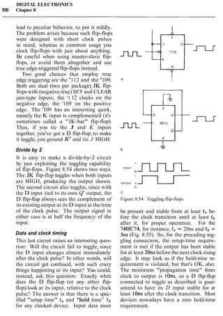
R8, i.e., 60mA quiescent current. That's in parallel with the impedance looking into
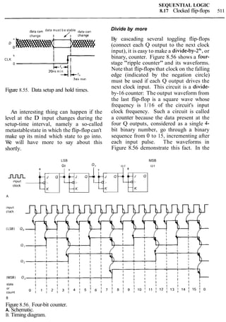
class AB operation, good for minimizing the base. The latter is hfe times twice
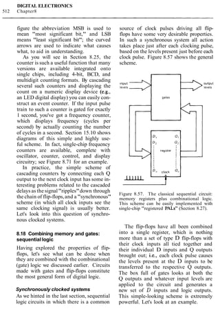
crossover distortion, at the cost of 1 watt the intrinsic emitter resistance the
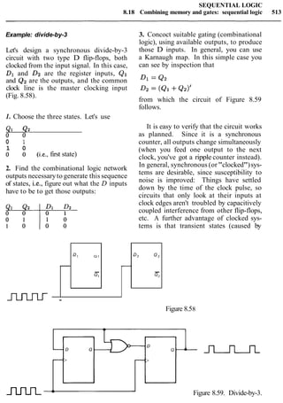
standby dissipation in each Output transis- impedance seen at Q27S emitter due to the
tor. feedback network at Q2's base. For hfe =
From the point of view of our earlier 250, zi, 250~[(2~25)+(3.3k/250)];
circuits, the only unusual feature is Q17s i.e., zin 16k.
quiescent collector voltage, one diode drop Output impedance: Since the imped-
below Vcc. That is where it must sit in ance looking back into Q3's collector is
order to hold Q3 in conduction, and the high, the output transistors are driven by
feedback path ensures that it will. (For a 1.5k source (R6). The output impedance
instance, if Q1 were to pull its ~ollector is about 15 ohms (hfe x 100) plus the 5
closer to ground, Q3 would conduct heav- ohm emitter resistance, or 20 ohms. The
ily, raising the output voltage, which in intrinsic emitter resistance of 0.4 ohm is
turn would force Q2to conduct more heav- negligible.
ily, reducing QI's collector current and Gain: The differential input stage sees
hence restoring the status quo.) R2 was a load of R2 paralleled by Q3's base re-
chosen to give a diode drop at QI's quies- sistance. Since Q3 is running lOmA quies-
cent current in order to keep the collector cent current, its intrinsic emitter resistance
currents in the differential pair approxi- is 2.5 ohms, giving a base impedance of
mately equal at the quiescent point. In about 250 ohms (again, hf, =loo). The
this transistor circuit the input bias current differential pair thus has a gain of
is not negligible (4pA), resulting in a 0.4
volt drop across the lOOk input resistors. 25011620
or 3.5
In transistor amplifier circuits like this, in 2 x
which the input currents are considerably The second stage, Q3, has a voltage gain of
larger than in op-amps, it is particularly 1.5W2.5ohms,or 600. The overall voltage](https://image.slidesharecdn.com/theartofelectronics-130527061117-phpapp01/85/The-art-of_electronics-188-320.jpg?cb=1674599069)
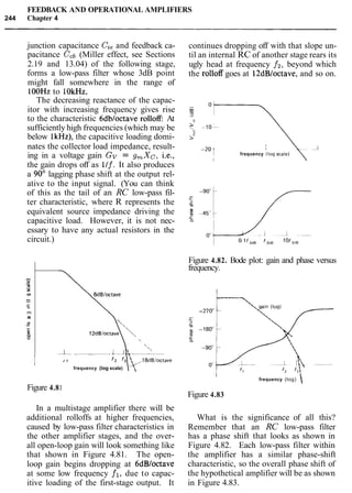
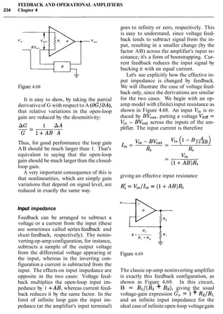
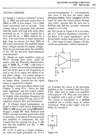
![FEEDBACK AMPLIFIER FREQUENCY COMPENSATION
4.35 Frequency response of the feedback network 247
so that the open-loop gain reaches 30dB
(rather than OdB) at the frequency of the
next natural pole of the op-amp. As the
graph shows, this means that the open-loop
gain is higher over most of the frequency
range, and the resultant amplifier will work
at higher frequencies. Some op-amps
are available in uncompensated versions
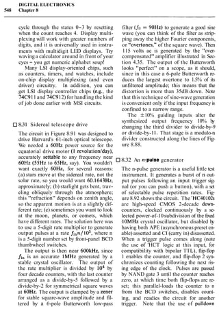
[e.g., the 748 is an uncompensated 741;
the same is true for the 308 (312), 3130
(3160), HA5102 (HA5112), etc.], with
recommended external capacitance values
for a selection of minimum closed-loop
gains. They are worth using if you need the
added bandwidth and your circuit operates
at high gain. An alternative is to use
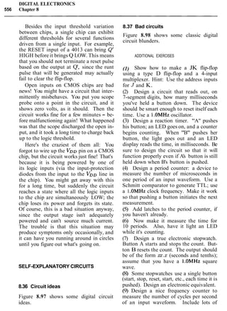
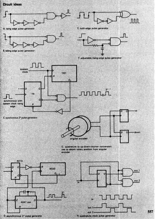
"decompensated" (a better word might be
"undercompensated") op-amps, such as
the 357, which are internally compensated
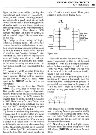
for closed-loop gains greater than some
minimum (Av> 5 in the case of the 357).
t -- -- -- -
I
frequency (log)
Figure 4.88
amplifier to move upward somewhat in
frequency, an effect known as "pole split-
ting." The frequency of the canceling zero
will be chosen accordingly.
4.35 Frequency response of the
feedback network
7Pole-zero compensation
It is possible to do a bit better than with
dominant-pole compensation by using a
compensation network that begins drop-
ping (6dB/octave, a "pole") at some low
frequency, then flattens out again (it has a
"zero") at the frequency of the second nat-
ural pole of the op-amp. In this way the
amplifier's second pole is "canceled,"giv-
ing a smooth 6dBloctave rolloff up to the
amplifier's third pole. Figure 4.88 shows
a frequency response plot. In practice,
the zero is chosen to cancel the amplifier's
second pole; then the position of the first
pole is adjusted so that the overall response
reaches unity gain at the frequency of the
amplifier's third pole. A good set of data
sheets will often give suggested component
values (an R and a C) for pole-zero com-
pensation, as well as the usual capacitor
values for dominant-pole compensation.
As you will see in Section 13.06, moving
the dominant pole downward in frequency
actually causes the second pole of the
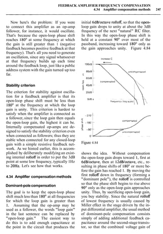
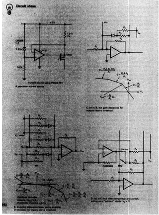
In all of the discussion thus far we have
assumed that the feedback network has
a flat frequency response; this is usually
the case, with the standard resistive volt-
age divider as a feedback network. How-
ever, there are occasions when some sort
of equalization amplifier is desired (inte-
grators and differentiators are in this cat-
egory) or when the frequency response of
the feedback network is modified to im-
prove amplifier stability. In such cases it
is important to remember that the Bode
plot of loop gain versus frequency is what
matters, rather than the curve of open-
loop gain. To make a long story short, the
curve of ideal closed-loop gain versus fre-
quency should intersect the curve of open-
loop gain, with a difference in slopes of
6dBloctave. As an example, it is com-
mon practice to put a small capacitor (a
few picofarads) across the feedback resis-
tor in the usual inverting or noninverting
amplifier. Figure 4.89 shows the circuit
and Bode plot.](https://image.slidesharecdn.com/theartofelectronics-130527061117-phpapp01/85/The-art-of_electronics-198-320.jpg?cb=1674599069)
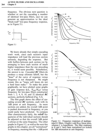
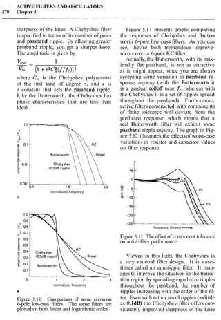
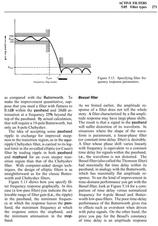
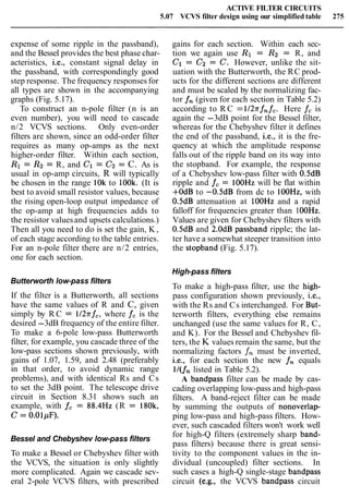
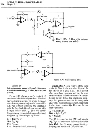
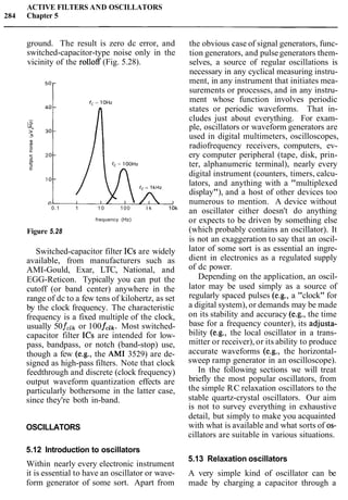
![ACTIVE FILTERS
5.02 Ideal performance with LC filters 265
frequency (kHz)
Figure 5.3. An unusually good passive bandpass filter implemented from inductorsand capacitors
(inductances in mH,capacitances in pF). Bottom: Measured response of the filter circuit. [Based
on Figs. 11 and 12 from Orchard, H. J., and Sheahan,D. E, ZEEE Journal of Solid-State Circuits,
Vol. SC-5, NO. 3 (1970).]
(or breakpoint, howeverdefined) is at a fre-
quency of 1 radian per second (or at 1Hz).
To determine the response of a filter whose
breakpoint is set at some other frequency,
simply multiply the values on the frequen-
cy axis by the actual breakpoint frequency
f,. In general, we will also stick to the
log-log graph of frequency response when
talking about filters, because it tells the
most about the frequency response. It
lets you see the approach to the ultimate
rolloff slope, and it permits you to read
off accurate values of attenuation. In this
case (cascaded RC sections) the normal-
ized graphs in Figures 5.2B and 5.2C dem-
onstrate the soft knee characteristic of pas-
sive RC filters.
5.02 Ideal performance with LC filters
As we pointed out in Chapter 1, filters
made with inductors and capacitors can
have very sharp responses. The parallel
LC resonant circuit is an example. By
including inductors in the design, it is pos-
sible to create filters with any desired flat-
ness of passband combined with sharpness
of transition and steepness of falloff out-
side the band. Figure 5.3 shows an exam-
ple of a telephone filter and its character-
istics.
Obviously the inclusion of inductors in-
to the design brings about some magic that
cannot be performed without them. In
the terminology of network analysis, that
magicconsists in the use of "off-axis poles."
Even so, the complexity of the filter in-
creases according to the required flatness
of passband and steepness of falloff outside
the band, accounting for the large number
of components used in the preceding fil-
ter. The transient response and phase-shift
characteristics are also generally degraded
as the amplitude response is improved to](https://image.slidesharecdn.com/theartofelectronics-130527061117-phpapp01/85/The-art-of_electronics-215-320.jpg?cb=1674599069)
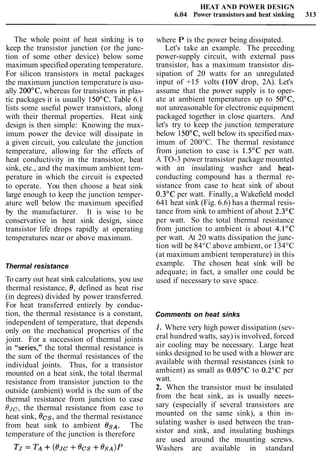
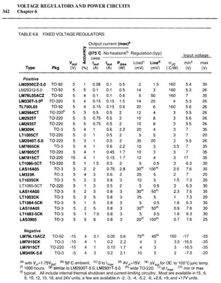
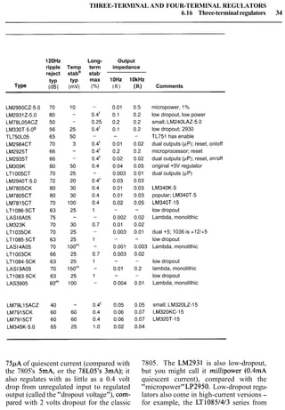
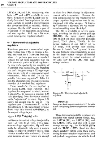
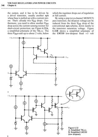
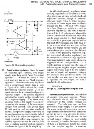
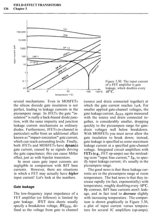
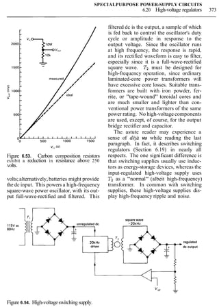
![THREE-TERMINAL AND FOUR-TERMINALREGULATORS
6.19 Switching regulators and dc-dc converters 355
in 317 out
ad;
- 1.2R
4I,,, = 1 . 2 5 1 ~ Figure 6.38. One amp current sources.
to sink current from a load returned to
ground (of course, you could always use
the negative-polarity 337, in the configu-
ration analogous to Fig. 6.38A).
National makes a special 3-terminal
device, the LM334, optimized for use as
a low-power current source. It comes
in the small plastic transistor package
(TO-92), as well as the standard DIP IC
package. You can use it all the way down
to lpA, becausethe"adj"current is a small
fraction of the total current. It has one
peculiarity,however: The output current is
temperature-dependent, in fact, precisely
proportional to absolute temperature. So
although it is not the world's most stable
current source, you can use it (Section
15.01) as a temperature sensor!
6.19 Switching regulators and
dc-dc converters
All the voltage regulator circuits we have
discussed so far work the same way: A
linear control element (the "pass transis-
tor") in series with the unregulated dc is
used, with feedback, to maintain constant
output voltage (or perhaps constant cur-
rent). The output voltage is always lower
in voltage than the unregulated input volt-
age, and some power is dissipated in
the control element [the average value of
I o u t ( K n - Vout),to be precise]. A minor
variation on this theme is the shunt regu-
lator, in which the control element is tied
from the output to ground, rather than in
series with the load; the simple resistor-
plus-zener is an example.
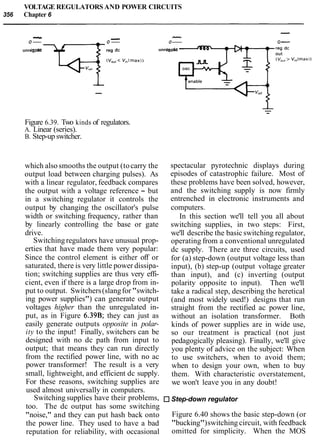
There is another way to generate a reg-
ulated dc voltage, fundamentally different
from what we've seen so far; look at Figure
6.39. In such a switching regulator a tran-
sistor operated as a saturated switch peri-
odically applies the full unregulated volt-
age across an inductor for short intervals.
The inductor's current builds up during
each pulse, storing ~ L I ~of energy in its
magnetic field; the stored energy is trans-
ferred to a filter capacitor at the output,](https://image.slidesharecdn.com/theartofelectronics-130527061117-phpapp01/85/The-art-of_electronics-305-320.jpg?cb=1674599069)

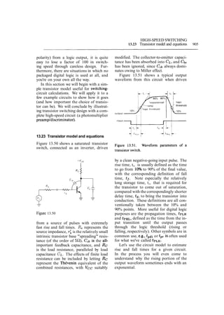
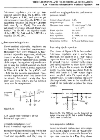
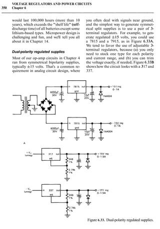
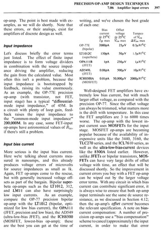
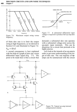
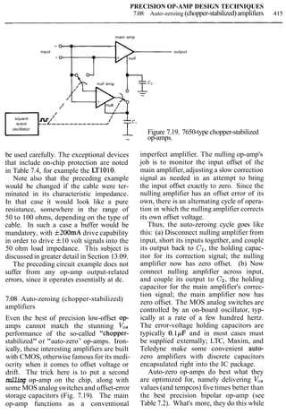
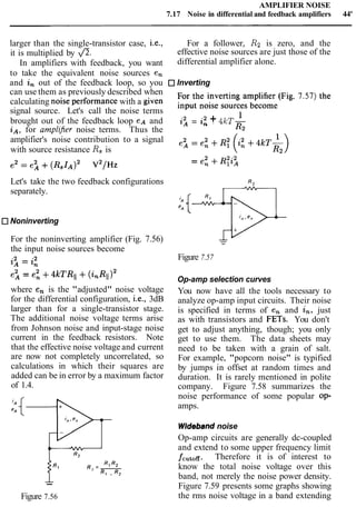
![PRECISION OP-AMP DESIGN TECHNIQUES
7.03 Example circuit: precision amplifier with automatic null offset 393
R , R8
100 Ok 10 Ok
0 01% 0 01%
500M
- cornpensatlon- -
'Plastic Capac~tors Inc , PD05-106 [orAmperex
C280MCH/A6M8 16 8fiF). TRW 8 6 3 11 OFF), or
ECC E42A105 K ( 1 OFF)]
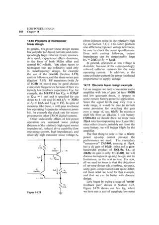
Figure 7.1. Autonulling dc laboratory amplifier.
Circuit description if desired. For now, just think of it as a
simple SPST switch.
The basic circuit is a follower (U1) driving When the logic input is HIGH ("auto-
an inverting amplifier of selectable gain zero"), the switch is closed, and U3charges
(U2), the latter offsettable by a signal the analog "memory" capacitor (GI) as
applied to its noninverting input. Q1 and necessary to maintain zero output. No
Q2 are FETs, used in this application as attempt is made to follow rapidly changing
simple analog switches; Q3-Q5 generate signals, since in the sort of application
suitable levels, from a logic-level input, for which this was designed the signals
to activate the switches. Q1 through Q5 are essentially dc, and some averaging
and their associated circuitry could all is a desirable feature. When the switch
be replaced by a relay, or even a switch, is opened, the voltage on the capacitor](https://image.slidesharecdn.com/theartofelectronics-130527061117-phpapp01/85/The-art-of_electronics-342-320.jpg?cb=1674599069)
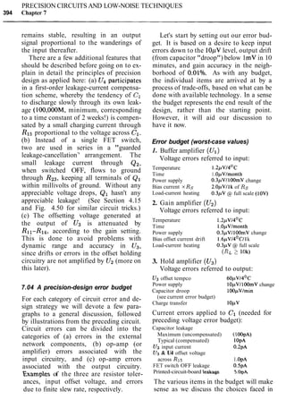
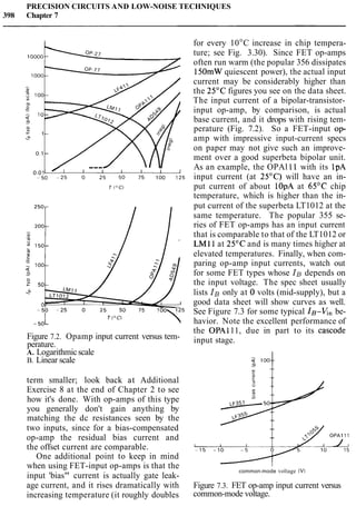
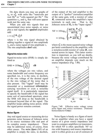
![PRECISION CIRCUITS AND LOW-NOISE TECHNIQUES
436 Chapter 7
temperature of the amplifier, for source
impedance R, .
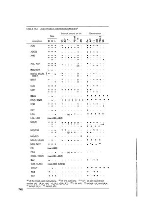
As we remarked earlier, noise figure
and noise temperature are simply different
ways of conveying the same information.
In fact, you can show that they are related
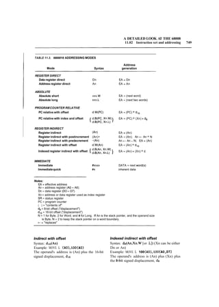
by the following expressions:
where T is the ambient temperature, usu-
ally taken as 290°K.
Generally speaking, good low-noise am-
plifiers have noise temperatures far below
room temperature (or, equivalently, they
have noise figures far less than 3dB). Later
in the chapter we will explain how you go
about measuring the noise figure (or tem-
perature) of an amplifier. First, however,
we need to understand noise in transis-
tors and the techniques of low-noise de-
sign. We hope the discussion that follows
will clarify what is often a murky sub-
ject!
After reading the next two sections, we
trust you won't ever be confused about
noise figure again!
7.13 Transistor amplifier voltage
and current noise
The noise generated by an amplifier is
easily described by a simple noise model
that is accurate enough for most purposes.- - -
In Figure 7.42, en represents a noise
voltage source in series with the input,
and in represents an input noise current.
The transistor (or amplifier, in general) is
assumed noiseless, and it simply amplifies
the input noise voltage it sees. That is, the
amplifier contributes a total noise voltage
e,, referred to the input, of
ea(rms)= [ef + (~.i,)~]: VIHZ:
generated by the amplifier's input noise
current passing through the source resis-
tance. Since the two noise terms are usu-
ally uncorrelated, their squared amplitudes
add to produce the effective noise voltage
seen by the amplifier. For low source re-
sistances the noise voltage en dominates,
whereas for high source impedances the
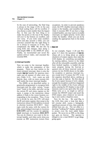
noise current in generally dominates.
Figure 7.42. Noise model of a transistor.
Just to give an idea of what these look
like, Figure 7.43 shows a graph of en and
in versus Ic and f , for a 2N5087. We'll
go into some detail now, describing these
and showing how to design for minimum
noise. It is worth noting that voltage noise
and current noise for a transistor are in the
range of nanovolts and picoamps per root
hertz (HZ*).
Voltage noise, en
The equivalent voltage noise looking in
series with the base of a transistor arises
from Johnson noise in the base spreading
resistance, rbb, and collector current shot
noise generating a noise voltage across the
intrinsic emitter resistance re. These two
terms look like this:
The two terms are simply the amplifier 2(w)2 v2/Hz
= 4kTrbb+-
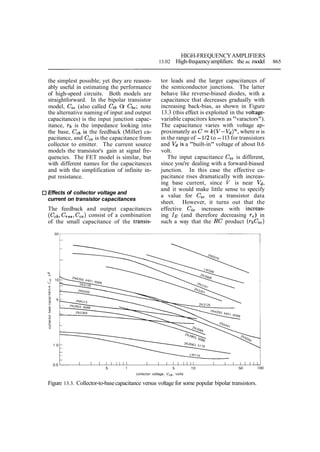
input noise voltage and the noise voltage QIC](https://image.slidesharecdn.com/theartofelectronics-130527061117-phpapp01/85/The-art-of_electronics-385-320.jpg?cb=1674599069)
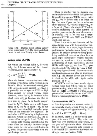
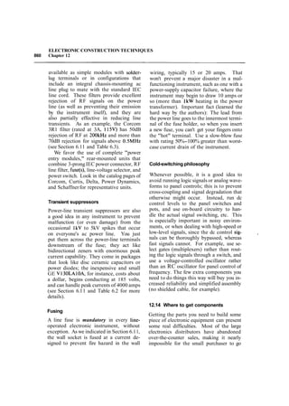
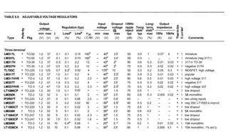
![TTL AND CMOS
8.11 Three-stateand open-collectordevices 489
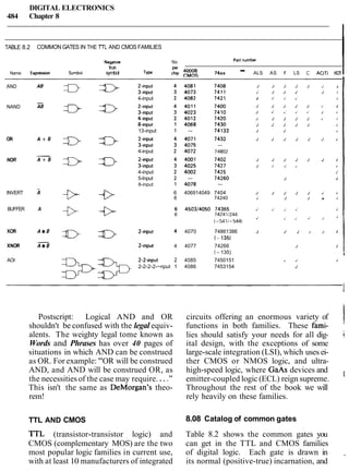
Dl
D2D3 ]data
A , 1a.r
A 2
read u control (read)
data 3 data2 data 1 data 0
Figure 8.20. Data bus.
data to be sent onto bus
2-input open-collector NANDs for the
three-state drivers of Figure 8.20, bringing
one input of each gate HIGH to enable the
gates onto the bus; note that the data then
asserted onto the bus are inverted. Each
bus line would need a resistive pullup to
A Q +5 volts.
symbol The disadvantage of open-collector
logic is that speed and noise immunity are
degraded, when compared with logic
constructed with active pullup devices,
because of the resistive pullup circuit.
That's why three-state drivers are nearly
universally favored for computer bus
- applications. However, there are three
situations in which you would choose
open-collector (or open-drain) devices:
driving external loads, "wired-OR," and
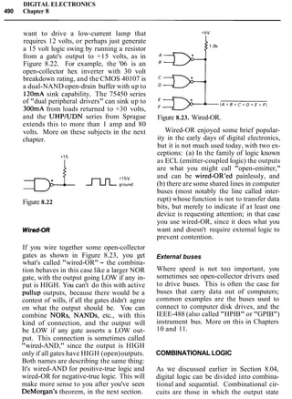
external buses. Let's look at them briefly.
Figure 8.21. LS TTL open-collector NAND.
Driving external loads
of the driver. Values of a few hundred
to a few thousand ohms are typical. If Open-collector logic is good for driving
you wanted to drive a bus with open- external loads that are returned to a
collector gates, you would substitute higher-voltage positive supply. You might](https://image.slidesharecdn.com/theartofelectronics-130527061117-phpapp01/85/The-art-of_electronics-437-320.jpg?cb=1674599069)
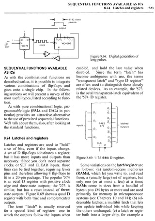
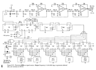
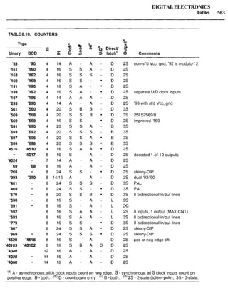
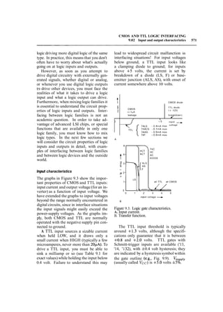
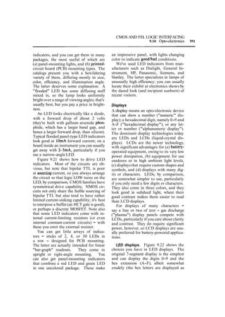
![SEQUENTIAL FUNCTIONS AVAILABLE AS ICs
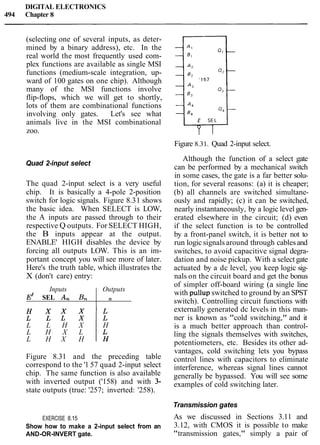
8.27 Sequential PALS 527
outputs
&
+CLK
I
RESET
input
'Ig4 (shift left)
Input
(shift r~ght) tI So S, A B C D ]
mode parallel-load
inputs: inputs
SHIFT R
LOAD
Figure 8.72. '194 4-bit bidirectional shift
register.
CLEAR can be either synchronous or jam-
load; for example, the '323 is the same as
the '299, but with synchronous clear.
Table 8.11 at the end of the chapter lists
the shift registers you're likely to use. As
always, not all types are available in all
logic families; be sure to check the data
books.
RAMSas shift registers
A random-access memory can always be
used as a shift register (but not vice versa)
by using an external counter to generate
successive addresses. Figure 8.73 shows
the idea. An 8-bit synchronous upldown
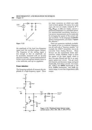
counter generates successive addresses for
a 256-wordx4-bit CMOS RAM. The com-
bination behaves like a quad 256-bit shift
register, with leftfright direction of shift
selected by the counter's UPIDOWN' con-
trol line. The other inputs of the counter
are shown enabled for counting. By choos-
ing a fast counter and memory, we were
able to achieve a maximum clocking rate
of 30MHz (see timing diagram), which
is the same as that of an integrated (but
much smaller) HC-type shift register. This
technique can be used to produce very
large shift registers, if desired.
EXERCISE 8.28
In the circuit of Figure 8.73, input data seem to
go into the same location that output data are
read from. Nevertheless, the circuit behaves
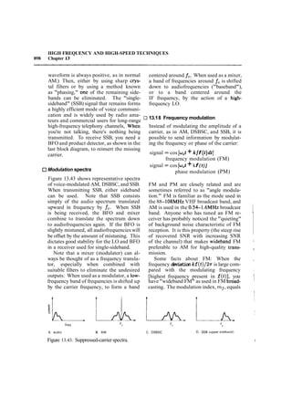
identically to a classic 256-word shift register.
Explain why.
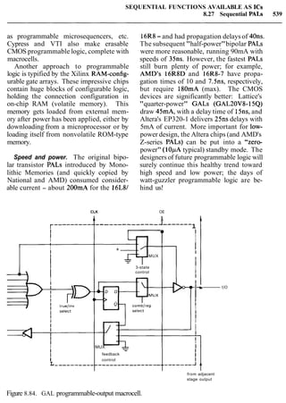
8.27 Sequential PALs
The combinational (gates-only) PALs we
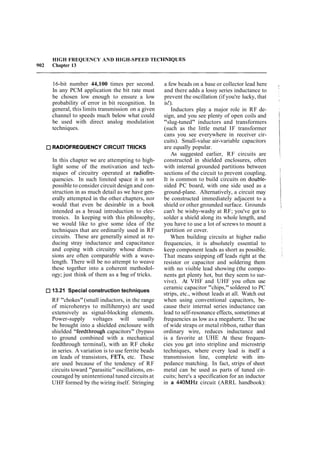
talked about in Section 8.15 belong to a
larger family that includes devices with
various numbers of on-chip D-type reg-
isters (called "registered PALS"). Typical
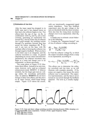
of these PALs is the 16R8, shown in Fig-
ure 8.74. The programmable-ANDffixed-
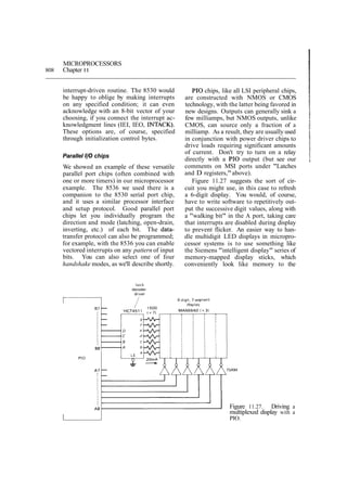
OR array typical of combinational PALS
generates the input levels for 8 synchro-
nously clocked D-type registers with three-
state outputs; the register outputs (and
their inverts) are available, along with the
standard input pins, as inputs to the logic
array. If you look back at Figure 8.57,
you'll see that a registered PAL is a general-
purpose sequential circuit element; within
limits set by the number of registers and
gates available, you can construct just
about anything you want. For instance,
yo](https://image.slidesharecdn.com/theartofelectronics-130527061117-phpapp01/85/The-art-of_electronics-475-320.jpg?cb=1674599069)