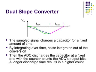
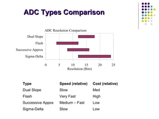
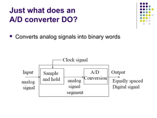
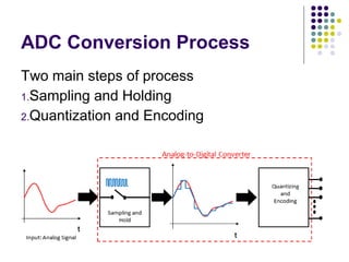
The content is related to Analog electronics. The prEsentation contains ADC process, Sampling and holding, Quantizing and encoding, Flash ADC, Pipeline ADC etc.
Simple description about the analog and digital signals
and a description about analog to digital conversion &
digital to analog conversion..............
This presentation contains the basic information you need to know about operational amplifier.
I have tried to cover all the basic info. If anything is left out or you have any suggestions i will appreciate it.
A complete description of including circuit diagram, gain equation, features of Instrumentational amplifier , its working principle, applications, practical circuits, Proteus simulation and conclusion.
Uet, Peshawar Pakistan
Batch-06
ADC - Analog to Digital Conversion on AVR microcontroller Atmega16Robo India
Robo India in this PPT is explaining on the most crucial and important aspect of Embedded system, robotics, automation and physical computing.
Analog to digital conversion is required in almost every project of above mentioned domain. One advantage to use a AVR micro controller is that it has inbuilt ADC thus we donot need to use external system for ADC.
Here Robo India is teaching how to use ADC in AVR series microcontrollers.
We welcome your views and queries, we are found at-
website: http://roboindia.com
mail- info@roboindia.com
This presentation illustrates the experience gained by me while working on fabricating a Successive Approximation ADC on a MOSIS chip. This was part of a project-oriented course at UT. The chip is currently being fabricated by MOSIS and will be available by mid-April for testing.
Sigma-Delta Analog to Digital ConvertersSatish Patil
In recent years Sigma-Delta ADCs became one of the most popular types of Analog-to-Digital converters. The key features of these are high-speed, high resolution and low operating voltages. These are commonly used in variety of applications like digital audio CDs, CODEC, biomedical sensor applications and wireless transmitters/receivers. The basic principles involved in this technique are oversampling and noise shaping. This report reviews different techniques proposed for high resolution, low power Sigma-Delta ADC. Conventional design of SDM was dominated by discrete time architecture but in modern designs continuous types are also becoming famous because of their low power attributes. Continuous efforts have been taken to reduce the supply voltages of SDM and recently, lowest reported is 250mv.
Frequency Modulation In Data TransmissionBise Mond
This presentation includes concepts of FM, generation of FM, transmission, reception, with the concepts of stereo FM and some basic circuitry of receiver and transmitter system.
This presentation is about AUTOSAR CAN stack. it provides an overview about:
- Included modules
- How modules communicate with each other
- Transmission and reception of frames
- changing network states
please let me know in the comments if you have any enhancements or feedback.
Ethnobotany and Ethnopharmacology:
Ethnobotany in herbal drug evaluation,
Impact of Ethnobotany in traditional medicine,
New development in herbals,
Bio-prospecting tools for drug discovery,
Role of Ethnopharmacology in drug evaluation,
Reverse Pharmacology.
How to Split Bills in the Odoo 17 POS ModuleCeline George
Bills have a main role in point of sale procedure. It will help to track sales, handling payments and giving receipts to customers. Bill splitting also has an important role in POS. For example, If some friends come together for dinner and if they want to divide the bill then it is possible by POS bill splitting. This slide will show how to split bills in odoo 17 POS.
This is a presentation by Dada Robert in a Your Skill Boost masterclass organised by the Excellence Foundation for South Sudan (EFSS) on Saturday, the 25th and Sunday, the 26th of May 2024.
He discussed the concept of quality improvement, emphasizing its applicability to various aspects of life, including personal, project, and program improvements. He defined quality as doing the right thing at the right time in the right way to achieve the best possible results and discussed the concept of the "gap" between what we know and what we do, and how this gap represents the areas we need to improve. He explained the scientific approach to quality improvement, which involves systematic performance analysis, testing and learning, and implementing change ideas. He also highlighted the importance of client focus and a team approach to quality improvement.
Instructions for Submissions thorugh G- Classroom.pptxJheel Barad
This presentation provides a briefing on how to upload submissions and documents in Google Classroom. It was prepared as part of an orientation for new Sainik School in-service teacher trainees. As a training officer, my goal is to ensure that you are comfortable and proficient with this essential tool for managing assignments and fostering student engagement.
2024.06.01 Introducing a competency framework for languag learning materials ...Sandy Millin
http://sandymillin.wordpress.com/iateflwebinar2024
Published classroom materials form the basis of syllabuses, drive teacher professional development, and have a potentially huge influence on learners, teachers and education systems. All teachers also create their own materials, whether a few sentences on a blackboard, a highly-structured fully-realised online course, or anything in between. Despite this, the knowledge and skills needed to create effective language learning materials are rarely part of teacher training, and are mostly learnt by trial and error.
Knowledge and skills frameworks, generally called competency frameworks, for ELT teachers, trainers and managers have existed for a few years now. However, until I created one for my MA dissertation, there wasn’t one drawing together what we need to know and do to be able to effectively produce language learning materials.
This webinar will introduce you to my framework, highlighting the key competencies I identified from my research. It will also show how anybody involved in language teaching (any language, not just English!), teacher training, managing schools or developing language learning materials can benefit from using the framework.
We all have good and bad thoughts from time to time and situation to situation. We are bombarded daily with spiraling thoughts(both negative and positive) creating all-consuming feel , making us difficult to manage with associated suffering. Good thoughts are like our Mob Signal (Positive thought) amidst noise(negative thought) in the atmosphere. Negative thoughts like noise outweigh positive thoughts. These thoughts often create unwanted confusion, trouble, stress and frustration in our mind as well as chaos in our physical world. Negative thoughts are also known as “distorted thinking”.
The Indian economy is classified into different sectors to simplify the analysis and understanding of economic activities. For Class 10, it's essential to grasp the sectors of the Indian economy, understand their characteristics, and recognize their importance. This guide will provide detailed notes on the Sectors of the Indian Economy Class 10, using specific long-tail keywords to enhance comprehension.
For more information, visit-www.vavaclasses.com
2. Presentation Outline
Introduction: Analog vs. Digital?
Examples of ADC Applications
Types of A/D Converters
A/D Subsystem used in the
microcontroller chip
Examples of Analog to Digital Signal
Conversion
Successive Approximation ADC
3. Analog Signals
Analog signals – directly measurable quantities
in terms of some other quantity
Examples:
Thermometer – mercury height rises as
temperature rises
Car Speedometer – Needle moves farther
right as you accelerate
Stereo – Volume increases as you turn the
knob.
4. Digital Signals
Digital Signals – have only two states. For
digital computers, we refer to binary states, 0
and 1. “1” can be on, “0” can be off.
Examples:
Light switch can be either on or off
Door to a room is either open or closed
5. Examples of A/D Applications
Microphones - take your voice varying pressure waves in the
air and convert them into varying electrical signals
Strain Gages - determines the amount of strain (change in
dimensions) when a stress is applied
Thermocouple – temperature measuring device converts
thermal energy to electric energy
Voltmeters
Digital Multimeters
6. Just what does an
A/D converter DO?
Converts analog signals into binary words
7. Two main steps of process
1.Sampling and Holding
2.Quantization and Encoding
ADC Conversion Process
8. Analog Digital Conversion
2-Step Process:
Quantizing - breaking down analog value is a
set of finite states
Encoding - assigning a digital word or
number to each state and matching it to the
input signal
9. Step 1: Quantizing
Example:
You have 0-10V
signals. Separate them
into a set of discrete
states with 1.25V
increments. (How did
we get 1.25V? See
next slide…)
Output
States
Discrete Voltage
Ranges (V)
0 0.00-1.25
1 1.25-2.50
2 2.50-3.75
3 3.75-5.00
4 5.00-6.25
5 6.25-7.50
6 7.50-8.75
7 8.75-10.0
10. Quantizing
The number of possible states that the
converter can output is:
N=2n
where n is the number of bits in the AD converter
Example: For a 3 bit A/D converter, N=23
=8.
Analog quantization size:
Q=(Vmax-Vmin)/N = (10V – 0V)/8 = 1.25V
11. Encoding
Here we assign the
digital value (binary
number) to each
state for the
computer to read.
Output
States
Output Binary Equivalent
0 000
1 001
2 010
3 011
4 100
5 101
6 110
7 111
12. Accuracy of A/D Conversion
There are two ways to best improve accuracy of
A/D conversion:
increasing the resolution which improves the
accuracy in measuring the amplitude of the
analog signal.
increasing the sampling rate which increases the
maximum frequency that can be measured.
13. Resolution
Resolution (number of discrete values the converter can
produce) = Analog Quantization size (Q)
(Q) = Vrange / 2^n, where Vrange is the range of analog
voltages which can be represented
limited by signal-to-noise ratio (should be around 6dB)
In our previous example: Q = 1.25V, this is a high
resolution. A lower resolution would be if we used a 2-bit
converter, then the resolution would be 10/2^2 = 2.50V.
15. SAMPLING
Sampling is the process of recording an
analog signal at regular discrete moments of
time.
The sampling rate fs is the number of
samples per second.
The time interval between samples is called
the sampling interval
Ts=1/fs.
16. The signal v(t)=cos(2πft) in Fig. 1 is sampled uniformly with 3 sampling intervals within each signal period T.
Therefore, the sampling interval Ts=T/3 and the sampling rate fs=3f.
17. The samples from above figure are shown as the sequence v[n] indexed by integer values of n.
18. NYQUIST THEOREM
The Nyquist-Shannon sampling theorem states that
“the sampling rate for exact recovery of a signal
composed of a sum of sinusoids is larger than twice
the maximum frequency of the signal”.
This rate is called the Nyquist sampling rate
fNyquist.
fs>fNyquist=2fmax(5)
19. QUANTIZATION
A sequence of samples like v[n] in Fig. 2 is not a
digital signal because the sample values can
potentially take on a continuous range of values.
In order to complete analog to digital conversion,
each sample value is mapped to a discrete level
(represented by a sequence of bits) in a process
called quantization.
In a m-bit quantizer, each quantization level is
represented with m bits, so that the number of
levels equals 2^m.
20. Overlaid on the samples v[n] from Fig. 2 is a 3-bit quantizer with 8 uniformly spaced quantization levels.
The quantizer approximates each sample value in v[n] to its nearest level value (shown on the left),
producing the quantized sequence vQ[n].
21.
22.
23. ADC Process
t
Continuous Signal
Sampling & Hold
Measuring analog signals
at uniform time intervals
Ideally twice as fast as what
we are sampling
Digital system works with
discrete states
Taking samples from each
location
Reflects sampled and hold
signal
Digital approximation
24. ADC Process
t
Sampling & Hold
Measuring analog signals
at uniform time intervals
Ideally twice as fast as what
we are sampling
Digital system works with
discrete states
Taking samples from each
location
Reflects sampled and hold
signal
Digital approximation
25. ADC Process
t
Sampling & Hold
Measuring analog signals
at uniform time intervals
Ideally twice as fast as what
we are sampling
Digital system works with
discrete states
Taking a sample from each
location
Reflects sampled and hold
signal
Digital approximation
26. ADC Process
t
Sampling & Hold
Measuring analog signals
at uniform time intervals
Ideally twice as fast as what
we are sampling
Digital system works with
discrete states
Taking samples from each
location
Reflects sampled and hold
signal
Digital approximation
27. Sampling Rate
Frequency at which ADC evaluates analog signal. As we
see in the second picture, evaluating the signal more often
more accurately depicts the ADC signal.
28. Aliasing
Occurs when the input signal is changing much
faster than the sample rate.
For example, a 2 kHz sine wave being sampled
at 1.5 kHz would be reconstructed as a 500 Hz
(the aliased signal) sine wave.
Nyquist Rule:
Use a sampling frequency at least twice as high
as the maximum frequency in the signal to avoid
aliasing.
29. Overall Better Accuracy
Increasing both the sampling rate and the resolution
you can obtain better accuracy in your AD signals.
31. Flash ADC
Consists of a series of comparators, each
one comparing the input signal to a unique
reference voltage.
The comparator outputs connect to the inputs
of a priority encoder circuit, which produces a
binary output
33. How Flash Works
As the analog input voltage exceeds the
reference voltage at each comparator, the
comparator outputs will sequentially saturate
to a high state.
The priority encoder generates a binary
number based on the highest-order active
input, ignoring all other active inputs.
35. Flash
Advantages
Simplest in terms of
operational theory
Most efficient in terms
of speed, very fast
limited only in terms of
comparator and gate
propagation delays
Disadvantages
Lower resolution
Expensive
For each additional
output bit, the number
of comparators is
doubled
i.e. for 8 bits, 256
comparators needed
36. Sigma Delta ADC
Over sampled input
signal goes to the
integrator
Output of integration is
compared to GND
Iterates to produce a
serial bit stream
Output is serial bit
stream with # of 1’s
proportional to Vin
39. Dual Slope Converter
The sampled signal charges a capacitor for a fixed
amount of time
By integrating over time, noise integrates out of the
conversion
Then the ADC discharges the capacitor at a fixed
rate with the counter counts the ADC’s output bits.
A longer discharge time results in a higher count
t
Vin
tFIX tmeas
40. Dual Slope Converter
Advantages
Input signal is averaged
Greater noise immunity
than other ADC types
High accuracy
Disadvantages
Slow
High precision external
components required to
achieve accuracy
41. Successive Approximation ADC
A Successive Approximation Register (SAR)
is added to the circuit
Instead of counting up in binary sequence,
this register counts by trying all values of bits
starting with the MSB and finishing at the
LSB.
The register monitors the comparators output
to see if the binary count is greater or less
than the analog signal input and adjusts the
bits accordingly
44. Successive Approximation
Advantages
Capable of high speed and
reliable
Medium accuracy compared
to other ADC types
Good tradeoff between
speed and cost
Capable of outputting the
binary number in serial (one
bit at a time) format.
Disadvantages
Higher resolution
successive approximation
ADC’s will be slower
Speed limited to ~5Msps
45. ADC Resolution Comparison
0 5 10 15 20 25
Sigma-Delta
Successive Approx
Flash
Dual Slope
Resolution (Bits)
Type Speed (relative) Cost (relative)
Dual Slope Slow Med
Flash Very Fast High
Successive Appox Medium – Fast Low
Sigma-Delta Slow Low
ADC Types ComparisonADC Types Comparison
47. Successive Approximation
MSB (bit 9)
Divided Vref by 2
Compare Vref /2 with Vin
If Vin is greater than Vref /2 , turn MSB on (1)
If Vin is less than Vref /2 , turn MSB off (0)
Vin =0.6V and V=0.5
Since Vin>V, MSB = 1 (on)
48. Successive Approximation
Next Calculate MSB-1 (bit 8)
Compare Vin=0.6 V to V=Vref/2 + Vref/4= 0.5+0.25 =0.75V
Since 0.6<0.75, MSB is turned off
Calculate MSB-2 (bit 7)
Go back to the last voltage that caused it to be turned on
(Bit 9) and add it to Vref/8, and compare with Vin
Compare Vin with (0.5+Vref/8)=0.625
Since 0.6<0.625, MSB is turned off
49. Successive Approximation
Calculate the state of MSB-3 (bit 6)
Go to the last bit that caused it to be turned on (In
this case MSB-1) and add it to Vref/16, and
compare it to Vin
Compare Vin to V= 0.5 + Vref/16= 0.5625
Since 0.6>0.5625, MSB-3=1 (turned on)
51. DAC Performance Specifications
Monotonicity means that the magnitude
of the output voltage increases every time
the input digital code increases.
Absolute accuracy is the measure of the
DAC output voltage with respect to its
expected value.
51
54. DAC Performance Specifications
Relative accuracy is the deviation of the
actual from the ideal output voltage as a
fraction of the full-scale voltage.
Settling time is the time required for the
outputs to switch and settle within ±½ LSB
when the input switches form all 0s to all 1s.
54
55. DAC Performance Specifications
Gain error occurs when the output saturates
before reaching the maximum output code.
Linearity error is the deviation from a straight
line output with increasing digital input codes.
55
58. DAC Performance Specifications
Differential nonlinearity is the difference
between actual and expected step size
when the input code is changed by 1 LSB.
Offset error occurs when the DAC output
is not 0 V when the input code is all 0s.
58