Downloaded 52 times

This document discusses sample-and-hold (S/H) circuits. It explains that S/H circuits sample an analog input signal and hold its value for subsequent processing. The simplest S/H circuit uses an MOS transistor switch and hold capacitor. Switched op-amp based S/H circuits are also discussed. S/H circuits are used in applications like analog-to-digital converters and switched capacitor filters to accurately hold input values during conversion. The document covers the working, purpose, implementation and advantages/disadvantages of S/H circuits.
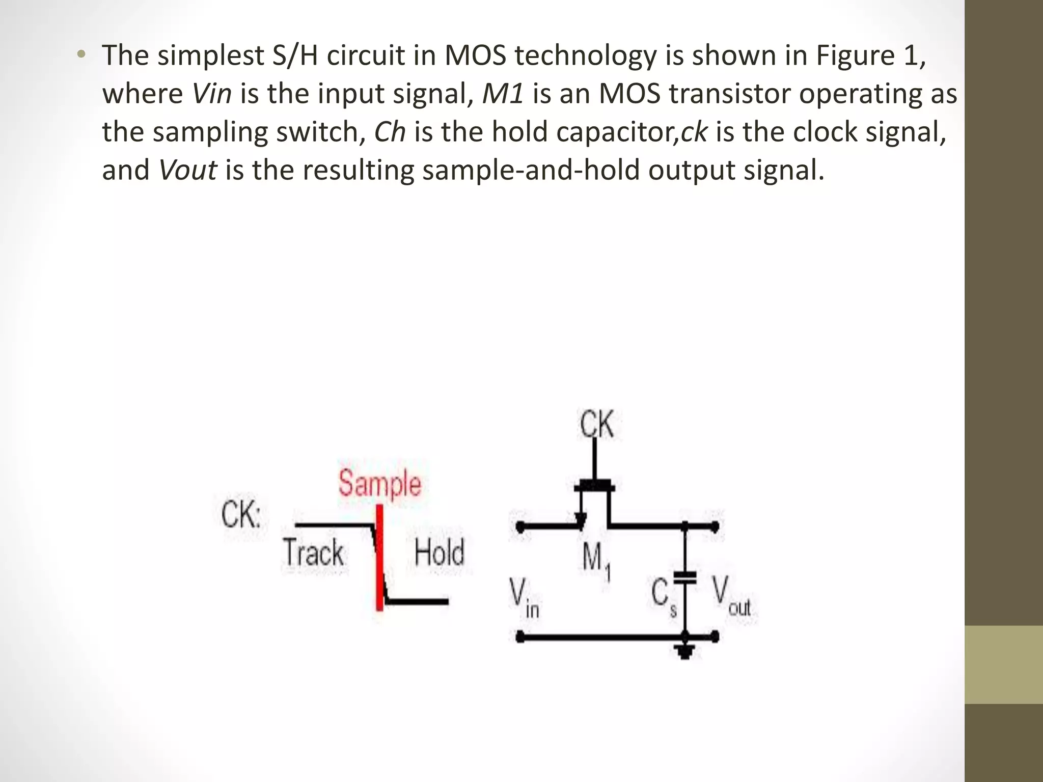
Introduction to Sample-and-hold (S/H) circuits and their functions in ADCs and filters.
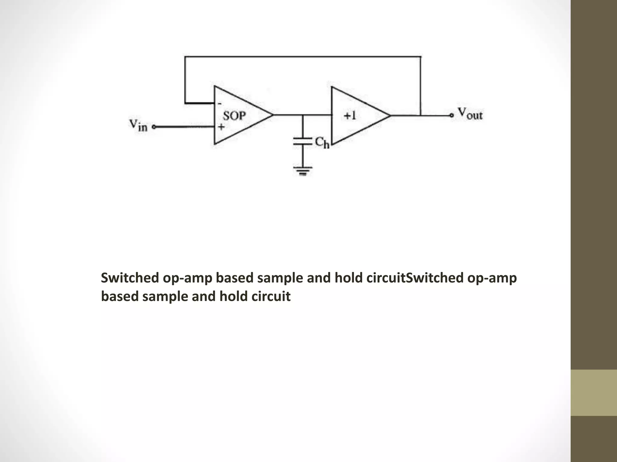
Working of switched op-amp based S/H circuits, detailing sample and hold modes.
Purpose of S/H circuits in analog-to-digital converters and simultaneous sampling.
Essential requirements for constant voltage holding, advantages, and disadvantages of S/H.
Summary of S/H circuit importance and need for new techniques for improved performance.


