Download to read offline
![Prity Yadav et al. Int. Journal of Engineering Research and Applications www.ijera.com
ISSN : 2248-9622, Vol. 4, Issue 10( Part - 3), October 2014, pp.120-122
www.ijera.com 121|P a g e
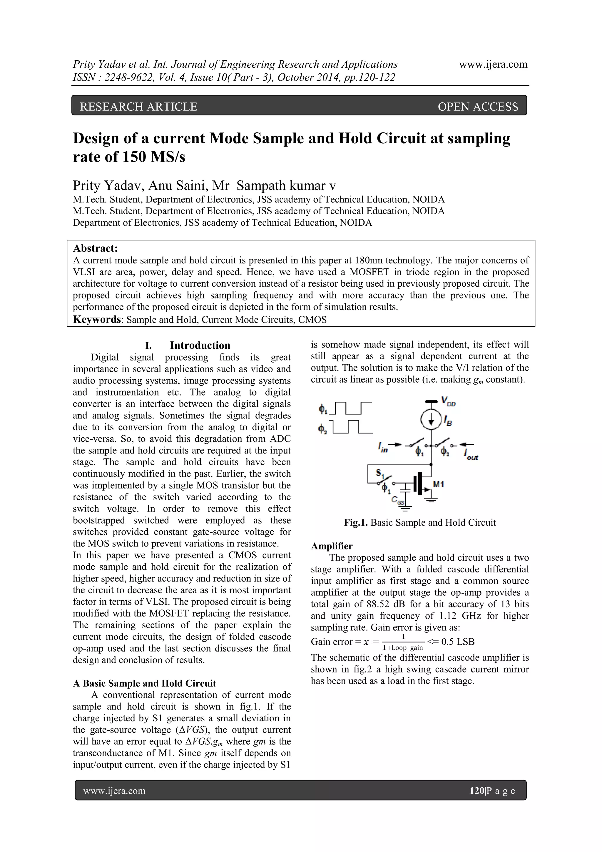
Fig.2 The two stage amplifier
The two stage operational amplifier has
differential input stage while it has a single ended
output. The first stage of the amplifier is differential
cascoded which produces a single ended output using
the current mirror load. The second stage of the
amplifier is common source amplifier with PMOS
load to attain high output swing.
In first stage the higher gain is achieved due to
differential cascode input stage while in second stage
the higher output swing is achieved whereas the gain
of output stage is not considerable and it is low.
Proposed Architecture of Sample and Hold
Circuit
The proposed architecture of the sample and hold
circuit is shown in fig.3.
Fig.3 Proposed Sample and Hold Circuit Schematic
During sampling phase (φ1), the capacitor is charged
up to VC=RIin. In the following hold phase, VC is
kept unchanged, and switch S3 connects R (The
parallel connected MOSFETs) to the next stage. The
on resistance of a MOSFET when (VDS << 2(VGS-
VTH)) is given as
𝑅𝑜𝑛 =
1
µCox (W/L)(Vgs − Vth)
Assuming the input of the next stage is held at VREF,
the output current in the hold mode will be the same
as input current at the end of the sampling mode, i.e.
Iout[n]=
Vref −Vo [n]
R+Ron
= Iin[n-1]
Where Ron is the on-resistance of the matched
switches S1 and S3 and Vo is the output voltage of
the amplifier. As all the switches within the circuit
are connected to a constant voltage, any variation in
the on resistance of the switches related to input
voltage level is removed. This, in turn, reduces the
overall distortion of the circuit. Furthermore, the
above property makes it possible to have a large and
constant gate-to-source voltage for each of the
switches. Therefore neither complimentary switches
nor clock boosting techniques are needed, provided
that the reference voltage (VREF) is properly selected.
II. Simulation Results
The input and output waveforms of the proposed
architecture is shown in the fig.4. The sampling
frequency is 150 MS/s and the frequency of input
current signal taken is 30 MHz with amplitude of
0.5mA.
Fig.4. Input and Output Waveforms of proposed
architecture
The following table (table.1) shows the specifications
of the amplifier designed for the presented current
mode sample and hold circuit.
Unity gain freq. (fu) 1.12GHz
Phase margin 55.2o
Power consumption 1.55mW
Output swing 1.2V @1.5V
CL 0.1pF
DC gain 88.52dB
Table.1. Amplifier specifications](https://image.slidesharecdn.com/r41003120122-141115041747-conversion-gate02/75/Design-of-a-current-Mode-Sample-and-Hold-Circuit-at-sampling-rate-of-150-MS-s-2-2048.jpg)
![Prity Yadav et al. Int. Journal of Engineering Research and Applications www.ijera.com
ISSN : 2248-9622, Vol. 4, Issue 10( Part - 3), October 2014, pp.120-122
www.ijera.com 122|P a g e
Fig.5 Gain and Phase Margin Plots of the amplifier
The gain of the proposed amplifier has higher gain
than the conventional as it approaches to 88.52dB
with a phase margin of 55.2 degrees. The switches
used in the design have dummy switches with
complementary clock input to reduce charge
injection. The width (W) of the dummy transistor has
been kept two times (2W) of the NMOS switch used.
Parameter Prev. design Proposed
Sampling freq. (Fs) 150MS/s 150MS/s
Power 3.7mW 3.42mW
Vdd 1.5V 1.5V
Bit resolution 12 bits 13 bits
Technology node 180nm 180nm
Table.1. Comparison with previous design
III. Conclusion
We have designed a two stage cascade amplifier
and a sample and hold circuit with higher gain and
less area in comparison to the previously proposed
sample and hold circuit [3] at 180nm technology. The
comparison shows that the design consumes less
power than previous design and has more resolution.
References
[1] A Current-mode CMOS Sample-and-Hold
Circuit for ADC. Fac. of Eng., King
Mongkut''s Inst. of Technol., Bangkok
; Kamsri, T. ; Petchmaneelumka,
W. ; Sungkabunchoo, T. 2001.
[2] G.K. Balachandran,P.E. Allen, “Switched-
Current Circuits in Digital CMOS
Technology With Low Charge-Injection
Errors,” IEEE J.Solid State Circuits, Vol.37,
p.1271, Oct. 2002
[3] A. Worapishet, J. B. Hughes, C. Toumazou,
“A. Low-Power High-Frequency Class-AB
Two-Step Sampling Switched-Current
Techniques,” IEEE Trans. Cir. and Syst. II,
Vol.50, p.649, Sep. 2003
[4] Sugimoto, Y. “A 1.5-V current-mode CMOS
sample-and-hold IC with 57-dB S/N at 20
MS/s and 54-dB S/N at 30 MS/s”; Dept. of
Electronics., Electron. & Communication.
Engg., Chuo Univ., Tokyo, Japan April 2001.
[5] Behnam Sedighi “A 1.5V 150MS/s Current-
Mode Sample-and-Hold Circuit” Department
of Electrical Engineering, Sharif University
of Technology, Tehran, IRAN
[6] X. Hu, K.W. Martin, “A Switched-Current
Sample-and-Hold Circuit,” IEEE J. Solid
State Circuits, Vol.32, p.898, June 1997
[7] P. J. Crawley and G. W. Roberts, “Predicting
harmonic distortion in switched- current
memory circuits”, IEEE trans. on Circuits and
Systems II: Analog and Digital Signal
Processing, vol. 41, No. 2, pp. 73-86, Feb.
1994.
[8] H. Yang, T. Fiez, and D. Allstot, “Current
feedthrough effects and cancellation
technique in switched-current circuits” In
IEEE Int. Symp. Circuits and systems, 1990,
PP.3186-3188.](https://image.slidesharecdn.com/r41003120122-141115041747-conversion-gate02/75/Design-of-a-current-Mode-Sample-and-Hold-Circuit-at-sampling-rate-of-150-MS-s-3-2048.jpg)

This paper presents a CMOS current mode sample and hold circuit designed for a sampling rate of 150 ms/s using 180nm technology, which improves area, power consumption, and accuracy compared to previous designs. The proposed architecture replaces resistors with MOSFETs in triode region for voltage to current conversion, achieving better performance and lower distortion. Simulation results demonstrate the circuit's high gain of 88.52 dB and efficient power usage, confirming its suitability for high-speed digital signal processing applications.


