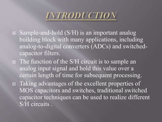
 Sample-and-hold (S/H) is an important analog
building block with many applications, including
analog-to-digital converters (ADCs) and switched-
capacitor filters.
 The function of the S/H circuit is to sample an
analog input signal and hold this value over a
certain length of time for subsequent processing.
 Taking advantages of the excellent properties of
MOS capacitors and switches, traditional switched
capacitor techniques can be used to realize different
S/H circuits .
 The simplest S/H circuit in MOS technology is
shown in Figure 1, where Vin is the input signal, M1
is an MOS transistor operating as the sampling
switch, Ch is the hold capacitor,ck is the clock
signal, and Vout is the resulting sample-and-hold
output signal.
Switched op-amp based sample and hold circuitSwitched op-amp
based sample and hold circuit
 During sample mode, the SOP behaves just like a
regular op-amp, in which the value of the output
follows the value of the input.
 During hold mode, the MOS transistors at the output
node of the SOP are turned off while they are still
operating in saturation, thus preventing any channel
charge from flowing into the output of the SOP.
 In addition, the SOP is shut off and its output is held
at high impedance, allowing the charge on Ch to be
preserved throughout the hold mode.
 On the other hand, the output buffer of this S/H
circuit is always operational during sample and hold
mode and is always providing the voltage on Ch to
the output of the S/H circuit.
 The sample and hold circuits are essentially used in
linear systems.
 In some kinds of analog-to-digital converters, the
input is often compared to a voltage generated
internally from a digital to analog converter D-A-C.
 The circuit tries a series of values and stops
converting once the voltages are "the same" within
some defined error margin.
 If the input value was permitted to change during
this comparison process, the resulting conversion
would be inaccurate and possibly completely
unrelated to the true input value. Such successive
approximation converters will often incorporate
internal sample and hold circuitry.
 In addition, sample and hold circuits are often used
when multiple samples need to be measured at the
same time. Each value is sampled and held, using a
common sample clock.
 In order that the input voltage is held constant for all
practical purposes, it is essential that the capacitor
have very low leakage, and that it not be loaded to
any significant degree which calls for a very high
input impedance.
 A true sample and hold circuit is connected to the
buffer for a short period of time; a track and hold
circuit is designed to track input continuously.
 - Obtain a low droop rate during holding mode
 - Stability is determined by the stabilities of OP
Amps.
 - OP Amps offset can constrain the accuracy of
SHA.
 Needs a special circuitry to stabilize the input
amplifier during the holding mode
 Sample-and-hold (S/H) is an important analog
building block that has many applications.
 The simplest S/H circuit can be constructed using
only one MOS transistor and one hold capacitor.
 However, due to the limitations of the MOS
transistor switches, errors due to charge injection
and clock feed through restrict the performance of
S/H circuits.
 As a result, different S/H techniques and
architectures are developed with the intention to
reduce or eliminate these errors.
 More new S/H techniques and architectures need to
be proposed in order to meet the increasing demand
for high-speed, low-power, and low voltage S/H
circuits for data acquisition systems.
Analog signal processing,

Analog signal processing,

  • 2.
     Sample-and-hold (S/H)is an important analog building block with many applications, including analog-to-digital converters (ADCs) and switched- capacitor filters.  The function of the S/H circuit is to sample an analog input signal and hold this value over a certain length of time for subsequent processing.  Taking advantages of the excellent properties of MOS capacitors and switches, traditional switched capacitor techniques can be used to realize different S/H circuits .
  • 3.
     The simplestS/H circuit in MOS technology is shown in Figure 1, where Vin is the input signal, M1 is an MOS transistor operating as the sampling switch, Ch is the hold capacitor,ck is the clock signal, and Vout is the resulting sample-and-hold output signal.
  • 4.
    Switched op-amp basedsample and hold circuitSwitched op-amp based sample and hold circuit
  • 5.
     During samplemode, the SOP behaves just like a regular op-amp, in which the value of the output follows the value of the input.  During hold mode, the MOS transistors at the output node of the SOP are turned off while they are still operating in saturation, thus preventing any channel charge from flowing into the output of the SOP.  In addition, the SOP is shut off and its output is held at high impedance, allowing the charge on Ch to be preserved throughout the hold mode.
  • 6.
     On theother hand, the output buffer of this S/H circuit is always operational during sample and hold mode and is always providing the voltage on Ch to the output of the S/H circuit.
  • 7.
     The sampleand hold circuits are essentially used in linear systems.  In some kinds of analog-to-digital converters, the input is often compared to a voltage generated internally from a digital to analog converter D-A-C.  The circuit tries a series of values and stops converting once the voltages are "the same" within some defined error margin.
  • 8.
     If theinput value was permitted to change during this comparison process, the resulting conversion would be inaccurate and possibly completely unrelated to the true input value. Such successive approximation converters will often incorporate internal sample and hold circuitry.  In addition, sample and hold circuits are often used when multiple samples need to be measured at the same time. Each value is sampled and held, using a common sample clock.
  • 9.
     In orderthat the input voltage is held constant for all practical purposes, it is essential that the capacitor have very low leakage, and that it not be loaded to any significant degree which calls for a very high input impedance.  A true sample and hold circuit is connected to the buffer for a short period of time; a track and hold circuit is designed to track input continuously.
  • 10.
     - Obtaina low droop rate during holding mode  - Stability is determined by the stabilities of OP Amps.  - OP Amps offset can constrain the accuracy of SHA.  Needs a special circuitry to stabilize the input amplifier during the holding mode
  • 11.
     Sample-and-hold (S/H)is an important analog building block that has many applications.  The simplest S/H circuit can be constructed using only one MOS transistor and one hold capacitor.  However, due to the limitations of the MOS transistor switches, errors due to charge injection and clock feed through restrict the performance of S/H circuits.  As a result, different S/H techniques and architectures are developed with the intention to reduce or eliminate these errors.
  • 12.
     More newS/H techniques and architectures need to be proposed in order to meet the increasing demand for high-speed, low-power, and low voltage S/H circuits for data acquisition systems.