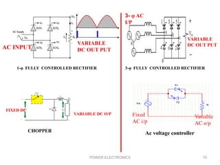
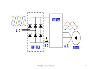
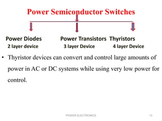
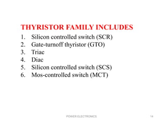
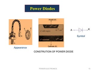
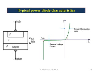
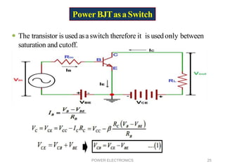
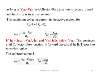
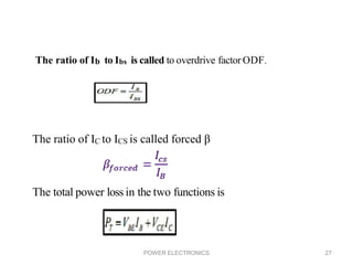
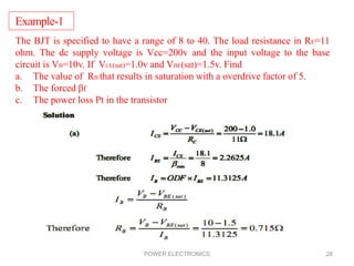
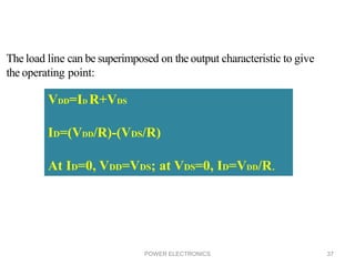
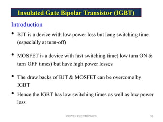
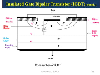
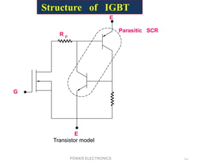
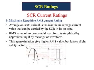
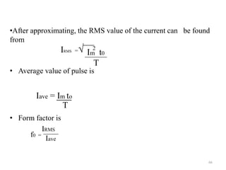
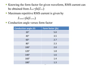
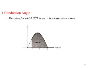
SlideShare a Scribd company logo
POWER ELECTRONICS (for R18 Regulation)
B.Tech – III year-I sem
BY
K. Sadanandam,
Assistant Professor( c )
Department of EEE,JNTUHCEM
POWER ELECTRONICS 1
POWER ELECTRONICS 2
SYLLABUS
UNIT-I
UNIT-II
POWER SWITCHING DEVICES
Concept of power electronics, scope and applications, types of power converters;
Power semiconductor switches and their V-I characteristics - Power Diodes, Power
BJT, SCR, Power MOSFET, Power IGBT; Thyristor ratings and protection, methods
of SCR commutation, UJT as a trigger source, gate drive circuits for BJT and
MOSFETs
AC-DC CONVERTERS (PHASE CONTROLLED RECTIFIERS)
Principles of single-phase fully-controlled converter with R, RL, and RLE load,
Principles of single-phase half-controlled converter with RL and RLE load, Principles
of three-phase fully-controlled converter operation with RLE load, Effect of load and
source inductances, General idea of gating circuits, Single phase and Three phase
dual converters
POWER ELECTRONICS 3
UNIT-III
DC-DC CONVERTERS (CHOPPER/SMPS)
Introduction, elementary chopper with an active switch and diode, concepts of duty
ratio, average inductor voltage, average capacitor current. Buck converter - Power
circuit, analysis and waveforms at steady state, duty ratio control of output voltage.
Boost converter - Power circuit, analysis and waveforms at steady state, relation
between duty ratio and average output voltage. Buck-Boost converter - Power circuit,
analysis and waveforms at steady state, relation between duty ratio and average
output voltage
UNIT-IV
AC-DC CONVERTERS (INVERTERS)
Introduction, principle of operation, performance parameters, single phase bridge
inverters with R, RL loads, 3-phase bridge inverters - 120 and 180 degrees mode of
operation, Voltage control of single phase inverters –single pulse width modulation,
multiple pulse width modulation, sinusoidal pulse width modulation
POWER ELECTRONICS 4
UNIT-V
AC-AC CONVERTERS
Phase Controller (AC Voltage Regulator)-Introduction, principle of operation of single
phase voltage controllers for R, R-L loads and its applications. Cyclo-converter-Principle of
operation of single phase cyclo-converters, relevant waveforms, circulating current mode of
operation, Advantages and disadvantages
.
POWER ELECTRONICS 5
TEXT BOOKS:
1. M. H. Rashid, “Power electronics: circuits, devices, and
applications”, Pearson Education India, 2009.
2. N. Mohan and T. M. Undeland, “Power Electronics:
Converters, Applications and Design”, JohnWiley & Sons,
2007.
REFERENCES:
1. R. W. Erickson and D. Maksimovic, “Fundamentals of
Power Electronics”, Springer Science & Business Media,
2007.
2. L. Umanand, “Power Electronics: Essentials and
Applications”, Wiley India, 2009.
CONTENT
• Course Objectives
• Course Outcomes
• Concept of power electronics
• Scope and applications
• Types of power converters
• Power semiconductor switches
• V-I characteristics of Power Diodes, Power BJT, SCR, Power
MOSFET, Power IGBT
• Thyristor ratings and protection, methods of SCR
commutation,
• UJT as a trigger source, gate drive circuits for BJT and
MOSFETs
POWER ELECTRONICS 6
POWER ELECTRONICS 7
•To Design/develop suitable power converter for efficient
control or conversion of power in drive Applications
• To Design / develop suitable power converter for efficient
transmission and utilization of power in power system
applications.
• To develop skills to build, and troubleshoot power
electronics circuits
•Foster ability to understand the use of power converters in
commercial and industrial applications.
COURSE OBJECTIVES
POWER ELECTRONICS 8
COURSE OUTCOMES
At the end of this course students will demonstrate the
ability to
•Understand the differences between signal level and power level
devices.
•Acquire knowledge about fundamental concepts and techniques
used in power electronics
•Analyze controlled rectifier circuits.
•Analyze the operation of DC-DC choppers.
•Analyze the operation of voltage source inverters
 Power Electronics is a field which combines Power (electric
power), Electronics and Control systems.
 Power electronics may be defined as the subject of
applications of solid state power semiconductor devices
(Thyristors) for the control and conversion of electric power.
 The power electronics subject deal about the conversion
and control of AC to DC ,DC to DC, AC to AC and DC
to AC
POWER ELECTRONICS 9
OVER VIEW OF POWER ELECTRONICS
POWER ELECTRONICS 10
AC INPUT
VARIABLE
DC OUT PUT
1-φ FULLY CONTROLLED RECTIFIER
3- φ AC
I/P
VARIABLE
DC OUT PUT
3-φ FULLY CONTROLLED RECTIFIER
FIXED DC
VARIABLE DC O/P
CHOPPER
Fixed
AC i/p
Variable
AC o/p
Ac voltage controller
POWER ELECTRONICS 11
1. COMMERCIAL APPLICATIONS: Heating Systems Ventilating, Air
Conditioners, Central Refrigeration, Lighting, Computers and Office
equipments, Uninterruptible Power Supplies (UPS), Elevators, and
Emergency Lamps.
2. DOMESTIC APPLICATIONS: Cooking Equipments, Lighting, Heating,
Air Conditioners, Refrigerators & Freezers, Personal Computers,
Entertainment Equipments, UPS.
3. INDUSTRIAL APPLICATIONS: Pumps, compressors, blowers and fans.
Machine tools, arc furnaces, induction furnaces, lighting control circuits,
industrial lasers, induction heating, welding equipments.
POWER ELECTRONICS 12
POWER ELECTRONIC APPLICATIONS
Power Semiconductor Switches
Power Diodes Power Transistors Thyristors
2 layer device 3 layer Device 4 layer Device
• Thyristor devices can convert and control large amounts of
power in AC or DC systems while using very low power for
control.
POWER ELECTRONICS 13
POWER ELECTRONICS 14
THYRISTOR FAMILY INCLUDES
1. Silicon controlled switch (SCR)
2. Gate-turnoff thyristor (GTO)
3. Triac
4. Diac
5. Silicon controlled switch (SCS)
6. Mos-controlled switch (MCT)
Power Diodes
POWER ELECTRONICS 15
Appearance
Symbol
CONSTRUTION OF POWER DIODE
KA
Typical power diode characteristics
POWER ELECTRONICS 16
Typical diode switching waveforms
POWER ELECTRONICS 17
POWER ELECTRONICS 18
POWER ELECTRONICS 19
1.Standard recovery
Reverse recovery time not specified, intended for 50/60Hz
2.Fast recovery and ultra-fast recovery
Reverse recovery time and recovered charge specified Intended for
converter applications
3.Schottky diode
A majority carrier device Essentially no recovered charge Model
with equilibrium i-v characteristic, in parallel with depletion region
capacitance Restricted to low voltage (few devices can block 100V
or more)
Types of power diodes
POWER ELECTRONICS 20
Power Transistors
Power transistors are classified as follows
1.Bipolar junction transistors(BJTs)
2.Metal-oxide semiconductor filed-effect transistors (MOSFETs)
3.Insulated-gate bipolar transistors(IGBTs)
POWER ELECTRONICS 21
POWER ELECTRONICS 22
BIPOLAR JUNCTION TRANSISTORS(BJTS)
POWER ELECTRONICS 23
Steady StateCharacteristics
CutoffRegion:When the base current (IB) is zero, the collector current
(IC) is insignificant and the transistor is driven into the cutoff region.
The transistor is now in the OFF state. The collector–base and base–
emitter junctions are reverse- biased in the cutoff region or OFF state,
and the transistor behaves as an open switch
In this region: IC= 0 and the collector–emitter voltage VCE is equal to the
supply voltageVCC
POWER ELECTRONICS 24
Saturation Region: When the base current is sufficient to drive the
transistor into saturation. During saturation, both junctions are
forward-biased and the transistor acts like a closed switch. In the
quasi saturation and hard saturation, the base drive is applied and
transistor is said to be on. In this region: IC = VCC /RC and VCE = zero
Active Region: In the active region, the collector–base junction is
reversed-biased and the base–emitter junction is forward-biased. The
active region of the transistor is mainly used for amplifier
applications and should be avoided for switching operation.
The power BJT is never operated in the active region (i.e. as an
amplifier) it is always operated between cut-off and saturation.
PowerBJTasaSwitch
 The transistor is usedasaswitch therefore it is usedonly between
saturation and cutoff.
POWER ELECTRONICS 25
POWER ELECTRONICS 26
as long as VCE>VBE the Collector-Base junction is reverse biased
and transistor is in active region,
The maximum collector current in the active region, for
If IB > IBM → VBE↑, IC↑ and VCE falls below VBE. This continues
until Collector-Base junction is forward biased and the BJT goes into
saturation region
The collector current is
POWER ELECTRONICS 27
The ratio of IC to ICS is called forced β
The total power loss in the two functions is
The ratio of Ib to Ibs is called to overdrive factor ODF.
POWER ELECTRONICS 28
Example-1
The BJT is specified to have a range of 8 to 40. The load resistance in RE=11
ohm. The dc supply voltage is Vcc=200v and the input voltage to the base
circuit is VB=10v. If VCE(sat)=1.0v and VBE(sat)=1.5v. Find
a. The value of RB that results in saturation with a overdrive factor of 5.
b. The forced βf
c. The power loss Pt in the transistor
POWER ELECTRONICS 29
(c)
Switching Characteristics
POWER ELECTRONICS 30
POWER ELECTRONICS 31
Switching Times – turn on
Input voltage rises from 0 to V1
Base current rises to IB1
Collector current begins to rise after the delay time, td
Collector current rises to steady-state value ICS
This “rise time”, tr allows the Miller capacitance to charge
to V1 turn on time, ton = td + tr
POWER ELECTRONICS 32
Input voltage changes from V1 to –V2
Base current changes to –IB2
Base current remains at –IB2 until the Miller
capacitance discharges to zero, storage time, ts
Base current falls to zero as Miller capacitance charges
to –V2, fall time, tf turn off time, toff = ts + tf
POWER ELECTRONICS 33
ADVANTAGES OF BJT’S
•BJT’s have high switching frequencies since their turn-on and turn-off
time is low.
•The turn-on losses of a BJT are small.
• BJT has controlled turn-on and turn-off characteristics since base
drive control is possible.
•BJT does not require commutation circuits.
DEMERITS OF BJT
•Drive circuit of BJT is complex.
•It has the problem of charge storage which sets a limit on switching
frequencies.
It cannot be used in parallel operation due to problems of negative
temperature coefficient
POWER ELECTRONICS 34
Metal-oxide semiconductor filed-effect transistors(MOSFETs)
Unlike the devices discussed so far, a power MOSFET is a
unipolar, majority carrier, “zero junction,” voltage-
controlled device. Figures (a) and (b) below show the
symbol of an N- type and P-type MOSFETs
MOSFETConstruction
POWER ELECTRONICS 35
POWER ELECTRONICS 36
V - I Characteristics of MOSFET
POWER ELECTRONICS 37
The load line can be superimposed on the output characteristic to give
the operating point:
VDD=ID R+VDS
ID=(VDD/R)-(VDS/R)
At ID=0, VDD=VDS; at VDS=0, ID=VDD/R.
Insulated Gate Bipolar Transistor (IGBT)
Introduction
• BJT is a device with low power loss but long switching time
(especially at turn-off)
• MOSFET is a device with fast switching time( low turn ON &
turn OFF times) but have high power losses
• The draw backs of BJT & MOSFET can be overcome by
IGBT
• Hence the IGBT has low switching times as well as low power
loss
POWER ELECTRONICS 38
POWER ELECTRONICS 39
Silicon
Dioxide
Silicon
Dioxide
Body
Region
Buffer
Layer
Injecting
Layer
Drain
drift
region
Drain
Gate
Source
J1
J2
J3
n+
n+
P+
n+
P
Construction of IGBT
Insulated Gate Bipolar Transistor (IGBT) (contd..)
POWER ELECTRONICS 40
Parasitic SCR
G
E
R p
E
Structure of IGBT
Transistor model
Structure of IGBT
• IGBT is combination of MOSFET & BJT on a single chip
• It contains P+ layer forms as a drain also called as Injecting
layer ,next layer n+ layer also called as Buffer Layer
• In between Injecting layer and Buffer layers a P-N junction J1 is
formed
POWER ELECTRONICS 41
• It also consists of another two junctions termed as J2 and J3
• This IGBT has a parasitic Thyristor as shown in FIG.2 (Both
PNP and NPN)
• Turn ON of this Thyristor is undesirable and the body of IGBT
is designed to avoid the turn ON
POWER ELECTRONICS 42
Construction of IGBT
POWER ELECTRONICS 43
• If IGBT does not have n+ layer, then the device is
called Non punch through IGBT (NPT-IGBT)
• If IGBT does not have n+ layer, then the device is
called Non punch through IGBT (NPT-IGBT)
Construction of IGBT
• N - Channel IGBT
• P - Channel IGBT
POWER ELECTRONICS 44
Types of IGBT
POWER ELECTRONICS 45
Gate
Source
( Emitter )
Drain
( Collector )
N-Channel IGBT
Gate
Source
( Emitter )
Drain
( Collector )
P- Channel IGBT
Types of IGBT (contd..)
FIG.3
FIG.4
V - I Characteristics of IGBT
Drain Characteristics Transfer characteristics
POWER ELECTRONICS
46
I
VGS2
VGS1
VGS3
BVDSS VDS
ID
VGS(th)
VRM
0 0 VGS
V - I Characteristics of IGBT
• The junction blocks reverse voltage. An IGBT without n+ buffer
layer has higher reverse blocking capability
• The reverse blocking voltage V RM on the V-I characteristics
• The junction J2 blocks forward voltage when IGBT is OFF
• BVDSS denotes the breakdown voltage in the forward direction
• Transfer characteristics of IGBT is similar to that power
MOSFET
POWER ELECTRONICS 47
SCR(silicon Controlled Rectifier
POWER ELECTRONICS 48
POWER ELECTRONICS 49
Threaded Stud
Anode ( aluminium)
Gate terminal Welded
to P region
J1
J2
J3
Cathode ( aluminium)
Construction of SCR
POWER ELECTRONICS 50
Anode
Gate
Cathode
J1
J2
J3
N
N
P
P
Anode
Gate
Cathode
Construction of SCR
Constructional of SCR
• SCR – is a Four layer, Three terminal, Three
P-N junction device
• Outer P region is Called Anode
• Outer N region is called Cathode
• Inner P region is called Gate
POWER ELECTRONICS 51
POWER ELECTRONICS 52
Switch-1
Switch-2
VDC
POWER ELECTRONICS 53
SCR Switching Characteristics
POWER ELECTRONICS 54
A
G
K
N
PP
P
N
N
Schematic Diagram
Two Transistor Analogy of SCR
Two transistor model of SCR is obtained by
splitting the two middle layers into two separate
parts.
• Emitter E of T1 is Anode, Emitter E of
T2 is Cathode
• Gate G is positive wrt Cathode.
POWER ELECTRONICS 55
P
P
N N
P
N
A
G
k
Two transistor Model
• Transistor T1 - PNP and Transistor T2 -NPN
Two Transistor Analogy of SCR (contd..)
POWER ELECTRONICS 56
Two transistor Model
J2
α1 , β 1
I a
I g
α2 , β2
A
K
G
IC2
I B1 = IC2
IB2
IC1
IK
Two Transistor Analogy of SCR (contd..)
POWER ELECTRONICS 57
During the OFF state of a transistor,
The collector Current, IC = α I E + I CBO
where
α – is the common base current gain
I CBO - Common base leakage Current
For transistor – 1
IC1 = α1 I E + I CBO1
Similarly for transistor - 2
IC2 = α2 I E + I CBO2
Two Transistor Analogy of SCR (contd..)
POWER ELECTRONICS 58
Total current I a - is sum of collector currents of two transistors.
I a = Ic1 + Ic2
When gate is triggered , I K = Ia + I g
I k = -----------------------------------------------------
( α1 I g + I CBO1 + I CBO2 )
( 1- (α1 + α2 )
Two Transistor Analogy of SCR (contd..)
POWER ELECTRONICS 59
V-I Characteristics of SCR
Vs
G
K
A
E
ES
Load
The Thyristor is connected as shown in circuit diagram
POWER ELECTRONICS 60
When Anode is made positive with respect to
Cathode and the switch is in open position the
Thyristor is said to be forward bias
During Forward Bias
A
G
K
J1
J2
J3
N
P
P
N
Forward Leakage
Current
Junction J1 , J 3 are forward bias and J2 is in
reverse bias
A small forward leakage current flows from Anode to
Cathode. At this position the Thyristor behaves like a “
Forward Blocking or OFF- State Condition ”
POWER ELECTRONICS 61
If the Anode to Cathode voltage is increased to sufficiently
large voltage , the junction J2 will breakdown. This is known
as “ Avalanche Breakdown ”
The voltage at which the junction- J2 gets break down is called
“ Forward Break Over Voltage ”
During Forward Bias (contd…)
POWER ELECTRONICS 62
During Reverse Bias
When Cathode is made positive with respect
to Anode and the switch is in open position
the Thyristor is said to be “ Reverse Bias ”
Junctions J1 , J 3 are reverse bias and J2 is in forward bias
A
G
J1
J2
J3
N
P
P
N
K
S
Reverse Leakage current
POWER ELECTRONICS
63
A small reverse leakage current flows from cathode to anode of
the order of few milliamperes or microamperes will flow. This is
known as “ Reverse Blocking or OFF- State Condition ” of
Thyristor.
If the reverse voltage is increased , then at a critical voltage
the Junctions J1 ,J 3 gets breakdown and the current increases
rapidly
Hence, a large magnitude of current flows through the
Thyristor and causes Thyristor gets damaged
During Reverse Bias (contd..)
Voltage
Current
0
Ig3 Ig2 Ig1
Ig =0
Holding Current
Latching Current
forward conduction
state ( on state )
forward leakage Current
Forward Blocking
Reverse leakage
Current
Reverse Blocking
V - I Characteristics of SCR
9EE604.2&3POWER ELECTRONICS 64
SCR Ratings
SCR Current Ratings
1- Maximum Repetitive RMS current Rating
• Average on-state current is the maximum average current
value that can be carried by the SCR in its on state.
• RMS value of non sinusoidal waveform is simplified by
approximating it by rectangular waveform.
• This approximation give higher RMS value, but leaves slight
safety factor.
65
• Average value of pulse is
• Form factor is
66
•After approximating, the RMS value of the current can be found
from
IRMS =√
Iave = Im to
T
f0 =
IRMS
Iave
Im t0
T
2
 Knowing the form factor for given waveform, RMS current can
be obtained from IRMS=fo(IAVE)
 Maximum repetitive RMS current is given by
IT(RMS)=fo(IT(AVE))
 Conduction angle verses form factor
67
Conduction angle (θ) Form factor (fo)
20° 5.0
40° 3.5
60° 2.7
80° 2.3
100° 2.0
120° 1.8
140° 1.6
160° 1.4
180° 1.3
1.Conduction Angle
• Duration for which SCR is on. It is measured as shown
68
2. Surge Current Rating
Peak anode current that SCR can handle for brief duration.
3. Latching current
Minimum anode current that must flow through the SCR in order
for it to stay on initially after gate signal is removed.
4. Holding Current
Minimum value of anode current, required to maintain SCR in
conducting state.
69
SCR Voltage Ratings
1. Peak repetitive forward blocking voltage
Maximum instantaneous voltage that SCR can block in
forward direction.
2. Peak Repetitive Reverse Voltage
Maximum instantaneous voltage that SCR can
withstand, without breakdown, in reverse direction.
3. Non-repetitive peak reverse voltage
Maximum transient reverse voltage that SCR can
withstand.
70
POWER ELECTRONICS 71
SCR Rate-of-Change Ratings
1.di/dt rating
Critical rate of rise of on-state current. It is the rate at which
anode current increases and must be less than rate at which
conduction area increases.
To prevent damage to SCR by high di/dt value, small inductance
is added in series with device.
2.dv/dt rating
Maximum rise time of a voltage pulse that can be applied to the
SCR in the off state without causing it to fire. Unscheduled firing
due to high value of dv/dt can be prevented by using RC snubber
circuit.
72
Gate Parameters
1.Maximum Gate Peak Inverse Voltage
Maximum value of negative DC voltage that can be applied without
damaging the gate-cathode junction.
2.Maximum Gate Trigger Current
Maximum DC gate current allowed to turn on the device.
3.Maximum gate trigger voltage
DC voltage necessary to produce maximum gate trigger current.
4.Maximum Gate Power Dissipation
Maximum instantaneous product of gate current and gate voltage
that can exist during forward-bias.
5. Minimum gate trigger voltage
Minimum DC gate-to-cathode voltage required to trigger the SCR.
6.Minimum gate trigger current
Minimum DC gate current necessary to turn SCR on.
73
What is Commutation?
The process of turning off an SCR is called commutation.
It is achieved by
1. Reducing anode current below holding current
2. Make anode negative with respect to cathode
Types of commutation are:
1. Natural or line commutation
2. Forced commutation
74
Methods of SCR commutation
POWER ELECTRONICS 75
1. Natural or line commutation
Natural commutation can be observed in AC voltage controllers,
phase controlled rectifiers and cyclo converter
POWER ELECTRONICS 76
 Class A: Self commutated by a resonating load
 Class B: Self commutated by an LC circuit
 Class C: C or L-C switched by another load carrying SCR
 Class D: C or L-C switched by an auxiliary SCR
 Class E: An external pulse source for commutation
 Class F: AC line commutation
Forced Commutation Methods
POWER ELECTRONICS 77
Class A: Self commutated by a resonating load
POWER ELECTRONICS 78
Class B: Self Commutated by an L-C Circuit
POWER ELECTRONICS 79
Class C: C or L-C switched by another load carrying SCR
POWER ELECTRONICS 80
Class D: L-C or C Switched by an Auxiliary SCR
POWER ELECTRONICS 81
Class E: External Pulse Source for Commutation
POWER ELECTRONICS 82
SCR R-triggering circuit
POWER ELECTRONICS 83
SCR RC-triggering circuit
POWER ELECTRONICS 84
SCR RC-triggering circuit
POWER ELECTRONICS 85
SCR trigger circuits using UJT oscillator
Circuit A Circuit B
POWER ELECTRONICS 86
Gate drive circuits for BJT
POWER ELECTRONICS 87
Gate drive circuits for MOSFET
POWER ELECTRONICS 88
POWER ELECTRONICS 89
CONCLUSION
•This unit discussed about the fundamental details of power
semiconductor switches and their V-I Characteristics, it helps
students to learn usage and application of switches into modeling
of various convertors and controllers.
THANQ
POWER ELECTRONICS 90

More Related Content

What's hot

Chapter 2 - Isolated DC-DC Converter.pdf
Chapter 2 - Isolated DC-DC Converter.pdfChapter 2 - Isolated DC-DC Converter.pdf
Chapter 2 - Isolated DC-DC Converter.pdfbenson215
 
Silicon controlled rectifier ( SCR )
Silicon controlled rectifier ( SCR )Silicon controlled rectifier ( SCR )
Silicon controlled rectifier ( SCR )DikshaTripathi20
 
Comparison of ac and dc transmission
Comparison of ac and dc transmissionComparison of ac and dc transmission
Comparison of ac and dc transmissionjawaharramaya
 
POWER ELECTRONIC DEVICES
POWER ELECTRONIC DEVICESPOWER ELECTRONIC DEVICES
POWER ELECTRONIC DEVICESshazaliza
 
Power electronics Phase Controlled Rectifiers - SCR
Power electronics   Phase Controlled Rectifiers - SCRPower electronics   Phase Controlled Rectifiers - SCR
Power electronics Phase Controlled Rectifiers - SCRBurdwan University
 
Unit 4 ac voltage controller
Unit 4 ac voltage controllerUnit 4 ac voltage controller
Unit 4 ac voltage controllerEr.Meraj Akhtar
 
Inverters (DC-AC)
Inverters (DC-AC)Inverters (DC-AC)
Inverters (DC-AC)Taimur Ijaz
 
Instrument transformer CT & PT
Instrument transformer CT & PTInstrument transformer CT & PT
Instrument transformer CT & PTChandan Singh
 
Dc Choppers
Dc ChoppersDc Choppers
Dc Choppersstooty s
 
Power Electronics-Introduction
Power Electronics-IntroductionPower Electronics-Introduction
Power Electronics-Introductionsangeetha rakhi
 
automatic voltage regulator
automatic voltage regulator automatic voltage regulator
automatic voltage regulator Sumit Patel
 
Lecture-1 : Introduction to Power Electronics
Lecture-1 : Introduction to Power ElectronicsLecture-1 : Introduction to Power Electronics
Lecture-1 : Introduction to Power Electronicsrsamurti
 
Power Electronics
Power Electronics Power Electronics
Power Electronics Mirza Baig
 

What's hot (20)

Chapter 2 - Isolated DC-DC Converter.pdf
Chapter 2 - Isolated DC-DC Converter.pdfChapter 2 - Isolated DC-DC Converter.pdf
Chapter 2 - Isolated DC-DC Converter.pdf
 
Thyristor
Thyristor Thyristor
Thyristor
 
Static relay
Static relayStatic relay
Static relay
 
DC DC Converter
DC DC ConverterDC DC Converter
DC DC Converter
 
Silicon controlled rectifier ( SCR )
Silicon controlled rectifier ( SCR )Silicon controlled rectifier ( SCR )
Silicon controlled rectifier ( SCR )
 
Comparison of ac and dc transmission
Comparison of ac and dc transmissionComparison of ac and dc transmission
Comparison of ac and dc transmission
 
POWER ELECTRONIC DEVICES
POWER ELECTRONIC DEVICESPOWER ELECTRONIC DEVICES
POWER ELECTRONIC DEVICES
 
Power flow through transmission line.
Power flow through transmission line.Power flow through transmission line.
Power flow through transmission line.
 
Power electronics Phase Controlled Rectifiers - SCR
Power electronics   Phase Controlled Rectifiers - SCRPower electronics   Phase Controlled Rectifiers - SCR
Power electronics Phase Controlled Rectifiers - SCR
 
Unit 4 ac voltage controller
Unit 4 ac voltage controllerUnit 4 ac voltage controller
Unit 4 ac voltage controller
 
cuk converter
cuk convertercuk converter
cuk converter
 
Inverters (DC-AC)
Inverters (DC-AC)Inverters (DC-AC)
Inverters (DC-AC)
 
Instrument transformer CT & PT
Instrument transformer CT & PTInstrument transformer CT & PT
Instrument transformer CT & PT
 
Power MOSFET
Power MOSFETPower MOSFET
Power MOSFET
 
Dc Choppers
Dc ChoppersDc Choppers
Dc Choppers
 
Power Electronics-Introduction
Power Electronics-IntroductionPower Electronics-Introduction
Power Electronics-Introduction
 
automatic voltage regulator
automatic voltage regulator automatic voltage regulator
automatic voltage regulator
 
Lecture-1 : Introduction to Power Electronics
Lecture-1 : Introduction to Power ElectronicsLecture-1 : Introduction to Power Electronics
Lecture-1 : Introduction to Power Electronics
 
Inverter
InverterInverter
Inverter
 
Power Electronics
Power Electronics Power Electronics
Power Electronics
 

Similar to POWER SWITCHING DEVICES

Chapter 1 Introduction to power Electronic Devices.pdf
Chapter 1 Introduction to power Electronic Devices.pdfChapter 1 Introduction to power Electronic Devices.pdf
Chapter 1 Introduction to power Electronic Devices.pdfLiewChiaPing
 
364615416-Power-Electronics.ppt
364615416-Power-Electronics.ppt364615416-Power-Electronics.ppt
364615416-Power-Electronics.pptPalashsamanta3
 
Lecture 1 Introduction of Power Electronics
Lecture 1 Introduction of Power ElectronicsLecture 1 Introduction of Power Electronics
Lecture 1 Introduction of Power Electronicsaadesharya
 
Basic Power Electronics Concepts_Ozipineci_ORNL.pdf
Basic Power Electronics Concepts_Ozipineci_ORNL.pdfBasic Power Electronics Concepts_Ozipineci_ORNL.pdf
Basic Power Electronics Concepts_Ozipineci_ORNL.pdfgulie
 
Single-Input Double Output High Efficient Boost Dc–Dc Converter
Single-Input Double Output High Efficient Boost Dc–Dc ConverterSingle-Input Double Output High Efficient Boost Dc–Dc Converter
Single-Input Double Output High Efficient Boost Dc–Dc ConverterIJMER
 
Introduction of power electronics and system.ppt
Introduction of power electronics and system.pptIntroduction of power electronics and system.ppt
Introduction of power electronics and system.pptalemaklil21
 
A Comparative Study of Various AC-DC Converters for Low Voltage Energy Harves...
A Comparative Study of Various AC-DC Converters for Low Voltage Energy Harves...A Comparative Study of Various AC-DC Converters for Low Voltage Energy Harves...
A Comparative Study of Various AC-DC Converters for Low Voltage Energy Harves...paperpublications3
 
MOSFET INVERTER SIMULATION
MOSFET INVERTER SIMULATIONMOSFET INVERTER SIMULATION
MOSFET INVERTER SIMULATIONMOHAMMAD HANNAN
 
power electronics digital notes.pdf
power electronics digital notes.pdfpower electronics digital notes.pdf
power electronics digital notes.pdfLucasMogaka
 
Introduction_to_Power_Electronics.ppt
Introduction_to_Power_Electronics.pptIntroduction_to_Power_Electronics.ppt
Introduction_to_Power_Electronics.pptssuser7598a2
 
Power Electronics Basic by Engr.Rajesh Roy
Power Electronics Basic by  Engr.Rajesh RoyPower Electronics Basic by  Engr.Rajesh Roy
Power Electronics Basic by Engr.Rajesh Royrajesh roy
 
Chapter 0 - Introduction.pdf
Chapter 0 - Introduction.pdfChapter 0 - Introduction.pdf
Chapter 0 - Introduction.pdfbenson215
 
MCTE4334 1 INTODUCTION.pptx
MCTE4334 1 INTODUCTION.pptxMCTE4334 1 INTODUCTION.pptx
MCTE4334 1 INTODUCTION.pptxAshSkyline1
 
Introduction to Power Electronics
Introduction to Power ElectronicsIntroduction to Power Electronics
Introduction to Power ElectronicsPaulTheHuman1
 
pdfcoffee.com_power-electronics-er-faruk-bin-poyen-dept-of-aeie-uit-bu-burdwa...
pdfcoffee.com_power-electronics-er-faruk-bin-poyen-dept-of-aeie-uit-bu-burdwa...pdfcoffee.com_power-electronics-er-faruk-bin-poyen-dept-of-aeie-uit-bu-burdwa...
pdfcoffee.com_power-electronics-er-faruk-bin-poyen-dept-of-aeie-uit-bu-burdwa...Gopal Krishna Murthy C R
 

Similar to POWER SWITCHING DEVICES (20)

Chapter 1 Introduction to power Electronic Devices.pdf
Chapter 1 Introduction to power Electronic Devices.pdfChapter 1 Introduction to power Electronic Devices.pdf
Chapter 1 Introduction to power Electronic Devices.pdf
 
364615416-Power-Electronics.ppt
364615416-Power-Electronics.ppt364615416-Power-Electronics.ppt
364615416-Power-Electronics.ppt
 
POWER-ELECTRONICS.ppt
POWER-ELECTRONICS.pptPOWER-ELECTRONICS.ppt
POWER-ELECTRONICS.ppt
 
Lecture 1 Introduction of Power Electronics
Lecture 1 Introduction of Power ElectronicsLecture 1 Introduction of Power Electronics
Lecture 1 Introduction of Power Electronics
 
Basic Power Electronics Concepts_Ozipineci_ORNL.pdf
Basic Power Electronics Concepts_Ozipineci_ORNL.pdfBasic Power Electronics Concepts_Ozipineci_ORNL.pdf
Basic Power Electronics Concepts_Ozipineci_ORNL.pdf
 
Single-Input Double Output High Efficient Boost Dc–Dc Converter
Single-Input Double Output High Efficient Boost Dc–Dc ConverterSingle-Input Double Output High Efficient Boost Dc–Dc Converter
Single-Input Double Output High Efficient Boost Dc–Dc Converter
 
Introduction of power electronics and system.ppt
Introduction of power electronics and system.pptIntroduction of power electronics and system.ppt
Introduction of power electronics and system.ppt
 
Power Electronics Introduction
Power Electronics IntroductionPower Electronics Introduction
Power Electronics Introduction
 
File 5e8ed4ef42f92
File 5e8ed4ef42f92File 5e8ed4ef42f92
File 5e8ed4ef42f92
 
1. Introduction.pdf
1. Introduction.pdf1. Introduction.pdf
1. Introduction.pdf
 
A Comparative Study of Various AC-DC Converters for Low Voltage Energy Harves...
A Comparative Study of Various AC-DC Converters for Low Voltage Energy Harves...A Comparative Study of Various AC-DC Converters for Low Voltage Energy Harves...
A Comparative Study of Various AC-DC Converters for Low Voltage Energy Harves...
 
MOSFET INVERTER SIMULATION
MOSFET INVERTER SIMULATIONMOSFET INVERTER SIMULATION
MOSFET INVERTER SIMULATION
 
PEDC- unit 4.pptx
PEDC- unit  4.pptxPEDC- unit  4.pptx
PEDC- unit 4.pptx
 
power electronics digital notes.pdf
power electronics digital notes.pdfpower electronics digital notes.pdf
power electronics digital notes.pdf
 
Introduction_to_Power_Electronics.ppt
Introduction_to_Power_Electronics.pptIntroduction_to_Power_Electronics.ppt
Introduction_to_Power_Electronics.ppt
 
Power Electronics Basic by Engr.Rajesh Roy
Power Electronics Basic by  Engr.Rajesh RoyPower Electronics Basic by  Engr.Rajesh Roy
Power Electronics Basic by Engr.Rajesh Roy
 
Chapter 0 - Introduction.pdf
Chapter 0 - Introduction.pdfChapter 0 - Introduction.pdf
Chapter 0 - Introduction.pdf
 
MCTE4334 1 INTODUCTION.pptx
MCTE4334 1 INTODUCTION.pptxMCTE4334 1 INTODUCTION.pptx
MCTE4334 1 INTODUCTION.pptx
 
Introduction to Power Electronics
Introduction to Power ElectronicsIntroduction to Power Electronics
Introduction to Power Electronics
 
pdfcoffee.com_power-electronics-er-faruk-bin-poyen-dept-of-aeie-uit-bu-burdwa...
pdfcoffee.com_power-electronics-er-faruk-bin-poyen-dept-of-aeie-uit-bu-burdwa...pdfcoffee.com_power-electronics-er-faruk-bin-poyen-dept-of-aeie-uit-bu-burdwa...
pdfcoffee.com_power-electronics-er-faruk-bin-poyen-dept-of-aeie-uit-bu-burdwa...
 

Recently uploaded

HYDROPOWER - Hydroelectric power generation
HYDROPOWER - Hydroelectric power generationHYDROPOWER - Hydroelectric power generation
HYDROPOWER - Hydroelectric power generationRobbie Edward Sayers
 
Student information management system project report ii.pdf
Student information management system project report ii.pdfStudent information management system project report ii.pdf
Student information management system project report ii.pdfKamal Acharya
 
Top 13 Famous Civil Engineering Scientist
Top 13 Famous Civil Engineering ScientistTop 13 Famous Civil Engineering Scientist
Top 13 Famous Civil Engineering Scientistgettygaming1
 
Hybrid optimization of pumped hydro system and solar- Engr. Abdul-Azeez.pdf
Hybrid optimization of pumped hydro system and solar- Engr. Abdul-Azeez.pdfHybrid optimization of pumped hydro system and solar- Engr. Abdul-Azeez.pdf
Hybrid optimization of pumped hydro system and solar- Engr. Abdul-Azeez.pdffxintegritypublishin
 
RS Khurmi Machine Design Clutch and Brake Exercise Numerical Solutions
RS Khurmi Machine Design Clutch and Brake Exercise Numerical SolutionsRS Khurmi Machine Design Clutch and Brake Exercise Numerical Solutions
RS Khurmi Machine Design Clutch and Brake Exercise Numerical SolutionsAtif Razi
 
ASME IX(9) 2007 Full Version .pdf
ASME IX(9)  2007 Full Version       .pdfASME IX(9)  2007 Full Version       .pdf
ASME IX(9) 2007 Full Version .pdfAhmedHussein950959
 
power quality voltage fluctuation UNIT - I.pptx
power quality voltage fluctuation UNIT - I.pptxpower quality voltage fluctuation UNIT - I.pptx
power quality voltage fluctuation UNIT - I.pptxViniHema
 
Explosives Industry manufacturing process.pdf
Explosives Industry manufacturing process.pdfExplosives Industry manufacturing process.pdf
Explosives Industry manufacturing process.pdf884710SadaqatAli
 
Event Management System Vb Net Project Report.pdf
Event Management System Vb Net  Project Report.pdfEvent Management System Vb Net  Project Report.pdf
Event Management System Vb Net Project Report.pdfKamal Acharya
 
LIGA(E)11111111111111111111111111111111111111111.ppt
LIGA(E)11111111111111111111111111111111111111111.pptLIGA(E)11111111111111111111111111111111111111111.ppt
LIGA(E)11111111111111111111111111111111111111111.pptssuser9bd3ba
 
Cloud-Computing_CSE311_Computer-Networking CSE GUB BD - Shahidul.pptx
Cloud-Computing_CSE311_Computer-Networking CSE GUB BD - Shahidul.pptxCloud-Computing_CSE311_Computer-Networking CSE GUB BD - Shahidul.pptx
Cloud-Computing_CSE311_Computer-Networking CSE GUB BD - Shahidul.pptxMd. Shahidul Islam Prodhan
 
The Benefits and Techniques of Trenchless Pipe Repair.pdf
The Benefits and Techniques of Trenchless Pipe Repair.pdfThe Benefits and Techniques of Trenchless Pipe Repair.pdf
The Benefits and Techniques of Trenchless Pipe Repair.pdfPipe Restoration Solutions
 
Toll tax management system project report..pdf
Toll tax management system project report..pdfToll tax management system project report..pdf
Toll tax management system project report..pdfKamal Acharya
 
Introduction to Casting Processes in Manufacturing
Introduction to Casting Processes in ManufacturingIntroduction to Casting Processes in Manufacturing
Introduction to Casting Processes in Manufacturingssuser0811ec
 
Final project report on grocery store management system..pdf
Final project report on grocery store management system..pdfFinal project report on grocery store management system..pdf
Final project report on grocery store management system..pdfKamal Acharya
 
Automobile Management System Project Report.pdf
Automobile Management System Project Report.pdfAutomobile Management System Project Report.pdf
Automobile Management System Project Report.pdfKamal Acharya
 
NO1 Pandit Amil Baba In Bahawalpur, Sargodha, Sialkot, Sheikhupura, Rahim Yar...
NO1 Pandit Amil Baba In Bahawalpur, Sargodha, Sialkot, Sheikhupura, Rahim Yar...NO1 Pandit Amil Baba In Bahawalpur, Sargodha, Sialkot, Sheikhupura, Rahim Yar...
NO1 Pandit Amil Baba In Bahawalpur, Sargodha, Sialkot, Sheikhupura, Rahim Yar...Amil baba
 
fundamentals of drawing and isometric and orthographic projection
fundamentals of drawing and isometric and orthographic projectionfundamentals of drawing and isometric and orthographic projection
fundamentals of drawing and isometric and orthographic projectionjeevanprasad8
 
Danfoss NeoCharge Technology -A Revolution in 2024.pdf
Danfoss NeoCharge Technology -A Revolution in 2024.pdfDanfoss NeoCharge Technology -A Revolution in 2024.pdf
Danfoss NeoCharge Technology -A Revolution in 2024.pdfNurvisNavarroSanchez
 
Online resume builder management system project report.pdf
Online resume builder management system project report.pdfOnline resume builder management system project report.pdf
Online resume builder management system project report.pdfKamal Acharya
 

Recently uploaded (20)

HYDROPOWER - Hydroelectric power generation
HYDROPOWER - Hydroelectric power generationHYDROPOWER - Hydroelectric power generation
HYDROPOWER - Hydroelectric power generation
 
Student information management system project report ii.pdf
Student information management system project report ii.pdfStudent information management system project report ii.pdf
Student information management system project report ii.pdf
 
Top 13 Famous Civil Engineering Scientist
Top 13 Famous Civil Engineering ScientistTop 13 Famous Civil Engineering Scientist
Top 13 Famous Civil Engineering Scientist
 
Hybrid optimization of pumped hydro system and solar- Engr. Abdul-Azeez.pdf
Hybrid optimization of pumped hydro system and solar- Engr. Abdul-Azeez.pdfHybrid optimization of pumped hydro system and solar- Engr. Abdul-Azeez.pdf
Hybrid optimization of pumped hydro system and solar- Engr. Abdul-Azeez.pdf
 
RS Khurmi Machine Design Clutch and Brake Exercise Numerical Solutions
RS Khurmi Machine Design Clutch and Brake Exercise Numerical SolutionsRS Khurmi Machine Design Clutch and Brake Exercise Numerical Solutions
RS Khurmi Machine Design Clutch and Brake Exercise Numerical Solutions
 
ASME IX(9) 2007 Full Version .pdf
ASME IX(9)  2007 Full Version       .pdfASME IX(9)  2007 Full Version       .pdf
ASME IX(9) 2007 Full Version .pdf
 
power quality voltage fluctuation UNIT - I.pptx
power quality voltage fluctuation UNIT - I.pptxpower quality voltage fluctuation UNIT - I.pptx
power quality voltage fluctuation UNIT - I.pptx
 
Explosives Industry manufacturing process.pdf
Explosives Industry manufacturing process.pdfExplosives Industry manufacturing process.pdf
Explosives Industry manufacturing process.pdf
 
Event Management System Vb Net Project Report.pdf
Event Management System Vb Net  Project Report.pdfEvent Management System Vb Net  Project Report.pdf
Event Management System Vb Net Project Report.pdf
 
LIGA(E)11111111111111111111111111111111111111111.ppt
LIGA(E)11111111111111111111111111111111111111111.pptLIGA(E)11111111111111111111111111111111111111111.ppt
LIGA(E)11111111111111111111111111111111111111111.ppt
 
Cloud-Computing_CSE311_Computer-Networking CSE GUB BD - Shahidul.pptx
Cloud-Computing_CSE311_Computer-Networking CSE GUB BD - Shahidul.pptxCloud-Computing_CSE311_Computer-Networking CSE GUB BD - Shahidul.pptx
Cloud-Computing_CSE311_Computer-Networking CSE GUB BD - Shahidul.pptx
 
The Benefits and Techniques of Trenchless Pipe Repair.pdf
The Benefits and Techniques of Trenchless Pipe Repair.pdfThe Benefits and Techniques of Trenchless Pipe Repair.pdf
The Benefits and Techniques of Trenchless Pipe Repair.pdf
 
Toll tax management system project report..pdf
Toll tax management system project report..pdfToll tax management system project report..pdf
Toll tax management system project report..pdf
 
Introduction to Casting Processes in Manufacturing
Introduction to Casting Processes in ManufacturingIntroduction to Casting Processes in Manufacturing
Introduction to Casting Processes in Manufacturing
 
Final project report on grocery store management system..pdf
Final project report on grocery store management system..pdfFinal project report on grocery store management system..pdf
Final project report on grocery store management system..pdf
 
Automobile Management System Project Report.pdf
Automobile Management System Project Report.pdfAutomobile Management System Project Report.pdf
Automobile Management System Project Report.pdf
 
NO1 Pandit Amil Baba In Bahawalpur, Sargodha, Sialkot, Sheikhupura, Rahim Yar...
NO1 Pandit Amil Baba In Bahawalpur, Sargodha, Sialkot, Sheikhupura, Rahim Yar...NO1 Pandit Amil Baba In Bahawalpur, Sargodha, Sialkot, Sheikhupura, Rahim Yar...
NO1 Pandit Amil Baba In Bahawalpur, Sargodha, Sialkot, Sheikhupura, Rahim Yar...
 
fundamentals of drawing and isometric and orthographic projection
fundamentals of drawing and isometric and orthographic projectionfundamentals of drawing and isometric and orthographic projection
fundamentals of drawing and isometric and orthographic projection
 
Danfoss NeoCharge Technology -A Revolution in 2024.pdf
Danfoss NeoCharge Technology -A Revolution in 2024.pdfDanfoss NeoCharge Technology -A Revolution in 2024.pdf
Danfoss NeoCharge Technology -A Revolution in 2024.pdf
 
Online resume builder management system project report.pdf
Online resume builder management system project report.pdfOnline resume builder management system project report.pdf
Online resume builder management system project report.pdf
 

POWER SWITCHING DEVICES

  • 1. POWER ELECTRONICS (for R18 Regulation) B.Tech – III year-I sem BY K. Sadanandam, Assistant Professor( c ) Department of EEE,JNTUHCEM POWER ELECTRONICS 1
  • 2. POWER ELECTRONICS 2 SYLLABUS UNIT-I UNIT-II POWER SWITCHING DEVICES Concept of power electronics, scope and applications, types of power converters; Power semiconductor switches and their V-I characteristics - Power Diodes, Power BJT, SCR, Power MOSFET, Power IGBT; Thyristor ratings and protection, methods of SCR commutation, UJT as a trigger source, gate drive circuits for BJT and MOSFETs AC-DC CONVERTERS (PHASE CONTROLLED RECTIFIERS) Principles of single-phase fully-controlled converter with R, RL, and RLE load, Principles of single-phase half-controlled converter with RL and RLE load, Principles of three-phase fully-controlled converter operation with RLE load, Effect of load and source inductances, General idea of gating circuits, Single phase and Three phase dual converters
  • 3. POWER ELECTRONICS 3 UNIT-III DC-DC CONVERTERS (CHOPPER/SMPS) Introduction, elementary chopper with an active switch and diode, concepts of duty ratio, average inductor voltage, average capacitor current. Buck converter - Power circuit, analysis and waveforms at steady state, duty ratio control of output voltage. Boost converter - Power circuit, analysis and waveforms at steady state, relation between duty ratio and average output voltage. Buck-Boost converter - Power circuit, analysis and waveforms at steady state, relation between duty ratio and average output voltage UNIT-IV AC-DC CONVERTERS (INVERTERS) Introduction, principle of operation, performance parameters, single phase bridge inverters with R, RL loads, 3-phase bridge inverters - 120 and 180 degrees mode of operation, Voltage control of single phase inverters –single pulse width modulation, multiple pulse width modulation, sinusoidal pulse width modulation
  • 4. POWER ELECTRONICS 4 UNIT-V AC-AC CONVERTERS Phase Controller (AC Voltage Regulator)-Introduction, principle of operation of single phase voltage controllers for R, R-L loads and its applications. Cyclo-converter-Principle of operation of single phase cyclo-converters, relevant waveforms, circulating current mode of operation, Advantages and disadvantages .
  • 5. POWER ELECTRONICS 5 TEXT BOOKS: 1. M. H. Rashid, “Power electronics: circuits, devices, and applications”, Pearson Education India, 2009. 2. N. Mohan and T. M. Undeland, “Power Electronics: Converters, Applications and Design”, JohnWiley & Sons, 2007. REFERENCES: 1. R. W. Erickson and D. Maksimovic, “Fundamentals of Power Electronics”, Springer Science & Business Media, 2007. 2. L. Umanand, “Power Electronics: Essentials and Applications”, Wiley India, 2009.
  • 6. CONTENT • Course Objectives • Course Outcomes • Concept of power electronics • Scope and applications • Types of power converters • Power semiconductor switches • V-I characteristics of Power Diodes, Power BJT, SCR, Power MOSFET, Power IGBT • Thyristor ratings and protection, methods of SCR commutation, • UJT as a trigger source, gate drive circuits for BJT and MOSFETs POWER ELECTRONICS 6
  • 7. POWER ELECTRONICS 7 •To Design/develop suitable power converter for efficient control or conversion of power in drive Applications • To Design / develop suitable power converter for efficient transmission and utilization of power in power system applications. • To develop skills to build, and troubleshoot power electronics circuits •Foster ability to understand the use of power converters in commercial and industrial applications. COURSE OBJECTIVES
  • 8. POWER ELECTRONICS 8 COURSE OUTCOMES At the end of this course students will demonstrate the ability to •Understand the differences between signal level and power level devices. •Acquire knowledge about fundamental concepts and techniques used in power electronics •Analyze controlled rectifier circuits. •Analyze the operation of DC-DC choppers. •Analyze the operation of voltage source inverters
  • 9.  Power Electronics is a field which combines Power (electric power), Electronics and Control systems.  Power electronics may be defined as the subject of applications of solid state power semiconductor devices (Thyristors) for the control and conversion of electric power.  The power electronics subject deal about the conversion and control of AC to DC ,DC to DC, AC to AC and DC to AC POWER ELECTRONICS 9 OVER VIEW OF POWER ELECTRONICS
  • 10. POWER ELECTRONICS 10 AC INPUT VARIABLE DC OUT PUT 1-φ FULLY CONTROLLED RECTIFIER 3- φ AC I/P VARIABLE DC OUT PUT 3-φ FULLY CONTROLLED RECTIFIER FIXED DC VARIABLE DC O/P CHOPPER Fixed AC i/p Variable AC o/p Ac voltage controller
  • 12. 1. COMMERCIAL APPLICATIONS: Heating Systems Ventilating, Air Conditioners, Central Refrigeration, Lighting, Computers and Office equipments, Uninterruptible Power Supplies (UPS), Elevators, and Emergency Lamps. 2. DOMESTIC APPLICATIONS: Cooking Equipments, Lighting, Heating, Air Conditioners, Refrigerators & Freezers, Personal Computers, Entertainment Equipments, UPS. 3. INDUSTRIAL APPLICATIONS: Pumps, compressors, blowers and fans. Machine tools, arc furnaces, induction furnaces, lighting control circuits, industrial lasers, induction heating, welding equipments. POWER ELECTRONICS 12 POWER ELECTRONIC APPLICATIONS
  • 13. Power Semiconductor Switches Power Diodes Power Transistors Thyristors 2 layer device 3 layer Device 4 layer Device • Thyristor devices can convert and control large amounts of power in AC or DC systems while using very low power for control. POWER ELECTRONICS 13
  • 14. POWER ELECTRONICS 14 THYRISTOR FAMILY INCLUDES 1. Silicon controlled switch (SCR) 2. Gate-turnoff thyristor (GTO) 3. Triac 4. Diac 5. Silicon controlled switch (SCS) 6. Mos-controlled switch (MCT)
  • 15. Power Diodes POWER ELECTRONICS 15 Appearance Symbol CONSTRUTION OF POWER DIODE KA
  • 16. Typical power diode characteristics POWER ELECTRONICS 16
  • 17. Typical diode switching waveforms POWER ELECTRONICS 17
  • 19. POWER ELECTRONICS 19 1.Standard recovery Reverse recovery time not specified, intended for 50/60Hz 2.Fast recovery and ultra-fast recovery Reverse recovery time and recovered charge specified Intended for converter applications 3.Schottky diode A majority carrier device Essentially no recovered charge Model with equilibrium i-v characteristic, in parallel with depletion region capacitance Restricted to low voltage (few devices can block 100V or more) Types of power diodes
  • 20. POWER ELECTRONICS 20 Power Transistors Power transistors are classified as follows 1.Bipolar junction transistors(BJTs) 2.Metal-oxide semiconductor filed-effect transistors (MOSFETs) 3.Insulated-gate bipolar transistors(IGBTs)
  • 22. POWER ELECTRONICS 22 BIPOLAR JUNCTION TRANSISTORS(BJTS)
  • 23. POWER ELECTRONICS 23 Steady StateCharacteristics CutoffRegion:When the base current (IB) is zero, the collector current (IC) is insignificant and the transistor is driven into the cutoff region. The transistor is now in the OFF state. The collector–base and base– emitter junctions are reverse- biased in the cutoff region or OFF state, and the transistor behaves as an open switch In this region: IC= 0 and the collector–emitter voltage VCE is equal to the supply voltageVCC
  • 24. POWER ELECTRONICS 24 Saturation Region: When the base current is sufficient to drive the transistor into saturation. During saturation, both junctions are forward-biased and the transistor acts like a closed switch. In the quasi saturation and hard saturation, the base drive is applied and transistor is said to be on. In this region: IC = VCC /RC and VCE = zero Active Region: In the active region, the collector–base junction is reversed-biased and the base–emitter junction is forward-biased. The active region of the transistor is mainly used for amplifier applications and should be avoided for switching operation. The power BJT is never operated in the active region (i.e. as an amplifier) it is always operated between cut-off and saturation.
  • 25. PowerBJTasaSwitch  The transistor is usedasaswitch therefore it is usedonly between saturation and cutoff. POWER ELECTRONICS 25
  • 26. POWER ELECTRONICS 26 as long as VCE>VBE the Collector-Base junction is reverse biased and transistor is in active region, The maximum collector current in the active region, for If IB > IBM → VBE↑, IC↑ and VCE falls below VBE. This continues until Collector-Base junction is forward biased and the BJT goes into saturation region The collector current is
  • 27. POWER ELECTRONICS 27 The ratio of IC to ICS is called forced β The total power loss in the two functions is The ratio of Ib to Ibs is called to overdrive factor ODF.
  • 28. POWER ELECTRONICS 28 Example-1 The BJT is specified to have a range of 8 to 40. The load resistance in RE=11 ohm. The dc supply voltage is Vcc=200v and the input voltage to the base circuit is VB=10v. If VCE(sat)=1.0v and VBE(sat)=1.5v. Find a. The value of RB that results in saturation with a overdrive factor of 5. b. The forced βf c. The power loss Pt in the transistor
  • 31. POWER ELECTRONICS 31 Switching Times – turn on Input voltage rises from 0 to V1 Base current rises to IB1 Collector current begins to rise after the delay time, td Collector current rises to steady-state value ICS This “rise time”, tr allows the Miller capacitance to charge to V1 turn on time, ton = td + tr
  • 32. POWER ELECTRONICS 32 Input voltage changes from V1 to –V2 Base current changes to –IB2 Base current remains at –IB2 until the Miller capacitance discharges to zero, storage time, ts Base current falls to zero as Miller capacitance charges to –V2, fall time, tf turn off time, toff = ts + tf
  • 33. POWER ELECTRONICS 33 ADVANTAGES OF BJT’S •BJT’s have high switching frequencies since their turn-on and turn-off time is low. •The turn-on losses of a BJT are small. • BJT has controlled turn-on and turn-off characteristics since base drive control is possible. •BJT does not require commutation circuits. DEMERITS OF BJT •Drive circuit of BJT is complex. •It has the problem of charge storage which sets a limit on switching frequencies. It cannot be used in parallel operation due to problems of negative temperature coefficient
  • 34. POWER ELECTRONICS 34 Metal-oxide semiconductor filed-effect transistors(MOSFETs) Unlike the devices discussed so far, a power MOSFET is a unipolar, majority carrier, “zero junction,” voltage- controlled device. Figures (a) and (b) below show the symbol of an N- type and P-type MOSFETs
  • 36. POWER ELECTRONICS 36 V - I Characteristics of MOSFET
  • 37. POWER ELECTRONICS 37 The load line can be superimposed on the output characteristic to give the operating point: VDD=ID R+VDS ID=(VDD/R)-(VDS/R) At ID=0, VDD=VDS; at VDS=0, ID=VDD/R.
  • 38. Insulated Gate Bipolar Transistor (IGBT) Introduction • BJT is a device with low power loss but long switching time (especially at turn-off) • MOSFET is a device with fast switching time( low turn ON & turn OFF times) but have high power losses • The draw backs of BJT & MOSFET can be overcome by IGBT • Hence the IGBT has low switching times as well as low power loss POWER ELECTRONICS 38
  • 40. POWER ELECTRONICS 40 Parasitic SCR G E R p E Structure of IGBT Transistor model
  • 41. Structure of IGBT • IGBT is combination of MOSFET & BJT on a single chip • It contains P+ layer forms as a drain also called as Injecting layer ,next layer n+ layer also called as Buffer Layer • In between Injecting layer and Buffer layers a P-N junction J1 is formed POWER ELECTRONICS 41
  • 42. • It also consists of another two junctions termed as J2 and J3 • This IGBT has a parasitic Thyristor as shown in FIG.2 (Both PNP and NPN) • Turn ON of this Thyristor is undesirable and the body of IGBT is designed to avoid the turn ON POWER ELECTRONICS 42 Construction of IGBT
  • 43. POWER ELECTRONICS 43 • If IGBT does not have n+ layer, then the device is called Non punch through IGBT (NPT-IGBT) • If IGBT does not have n+ layer, then the device is called Non punch through IGBT (NPT-IGBT) Construction of IGBT
  • 44. • N - Channel IGBT • P - Channel IGBT POWER ELECTRONICS 44 Types of IGBT
  • 45. POWER ELECTRONICS 45 Gate Source ( Emitter ) Drain ( Collector ) N-Channel IGBT Gate Source ( Emitter ) Drain ( Collector ) P- Channel IGBT Types of IGBT (contd..) FIG.3 FIG.4
  • 46. V - I Characteristics of IGBT Drain Characteristics Transfer characteristics POWER ELECTRONICS 46 I VGS2 VGS1 VGS3 BVDSS VDS ID VGS(th) VRM 0 0 VGS
  • 47. V - I Characteristics of IGBT • The junction blocks reverse voltage. An IGBT without n+ buffer layer has higher reverse blocking capability • The reverse blocking voltage V RM on the V-I characteristics • The junction J2 blocks forward voltage when IGBT is OFF • BVDSS denotes the breakdown voltage in the forward direction • Transfer characteristics of IGBT is similar to that power MOSFET POWER ELECTRONICS 47
  • 49. POWER ELECTRONICS 49 Threaded Stud Anode ( aluminium) Gate terminal Welded to P region J1 J2 J3 Cathode ( aluminium) Construction of SCR
  • 51. Constructional of SCR • SCR – is a Four layer, Three terminal, Three P-N junction device • Outer P region is Called Anode • Outer N region is called Cathode • Inner P region is called Gate POWER ELECTRONICS 51
  • 53. POWER ELECTRONICS 53 SCR Switching Characteristics
  • 54. POWER ELECTRONICS 54 A G K N PP P N N Schematic Diagram Two Transistor Analogy of SCR Two transistor model of SCR is obtained by splitting the two middle layers into two separate parts.
  • 55. • Emitter E of T1 is Anode, Emitter E of T2 is Cathode • Gate G is positive wrt Cathode. POWER ELECTRONICS 55 P P N N P N A G k Two transistor Model • Transistor T1 - PNP and Transistor T2 -NPN Two Transistor Analogy of SCR (contd..)
  • 56. POWER ELECTRONICS 56 Two transistor Model J2 α1 , β 1 I a I g α2 , β2 A K G IC2 I B1 = IC2 IB2 IC1 IK Two Transistor Analogy of SCR (contd..)
  • 57. POWER ELECTRONICS 57 During the OFF state of a transistor, The collector Current, IC = α I E + I CBO where α – is the common base current gain I CBO - Common base leakage Current For transistor – 1 IC1 = α1 I E + I CBO1 Similarly for transistor - 2 IC2 = α2 I E + I CBO2 Two Transistor Analogy of SCR (contd..)
  • 58. POWER ELECTRONICS 58 Total current I a - is sum of collector currents of two transistors. I a = Ic1 + Ic2 When gate is triggered , I K = Ia + I g I k = ----------------------------------------------------- ( α1 I g + I CBO1 + I CBO2 ) ( 1- (α1 + α2 ) Two Transistor Analogy of SCR (contd..)
  • 59. POWER ELECTRONICS 59 V-I Characteristics of SCR Vs G K A E ES Load The Thyristor is connected as shown in circuit diagram
  • 60. POWER ELECTRONICS 60 When Anode is made positive with respect to Cathode and the switch is in open position the Thyristor is said to be forward bias During Forward Bias A G K J1 J2 J3 N P P N Forward Leakage Current Junction J1 , J 3 are forward bias and J2 is in reverse bias A small forward leakage current flows from Anode to Cathode. At this position the Thyristor behaves like a “ Forward Blocking or OFF- State Condition ”
  • 61. POWER ELECTRONICS 61 If the Anode to Cathode voltage is increased to sufficiently large voltage , the junction J2 will breakdown. This is known as “ Avalanche Breakdown ” The voltage at which the junction- J2 gets break down is called “ Forward Break Over Voltage ” During Forward Bias (contd…)
  • 62. POWER ELECTRONICS 62 During Reverse Bias When Cathode is made positive with respect to Anode and the switch is in open position the Thyristor is said to be “ Reverse Bias ” Junctions J1 , J 3 are reverse bias and J2 is in forward bias A G J1 J2 J3 N P P N K S Reverse Leakage current
  • 63. POWER ELECTRONICS 63 A small reverse leakage current flows from cathode to anode of the order of few milliamperes or microamperes will flow. This is known as “ Reverse Blocking or OFF- State Condition ” of Thyristor. If the reverse voltage is increased , then at a critical voltage the Junctions J1 ,J 3 gets breakdown and the current increases rapidly Hence, a large magnitude of current flows through the Thyristor and causes Thyristor gets damaged During Reverse Bias (contd..)
  • 64. Voltage Current 0 Ig3 Ig2 Ig1 Ig =0 Holding Current Latching Current forward conduction state ( on state ) forward leakage Current Forward Blocking Reverse leakage Current Reverse Blocking V - I Characteristics of SCR 9EE604.2&3POWER ELECTRONICS 64
  • 65. SCR Ratings SCR Current Ratings 1- Maximum Repetitive RMS current Rating • Average on-state current is the maximum average current value that can be carried by the SCR in its on state. • RMS value of non sinusoidal waveform is simplified by approximating it by rectangular waveform. • This approximation give higher RMS value, but leaves slight safety factor. 65
  • 66. • Average value of pulse is • Form factor is 66 •After approximating, the RMS value of the current can be found from IRMS =√ Iave = Im to T f0 = IRMS Iave Im t0 T 2
  • 67.  Knowing the form factor for given waveform, RMS current can be obtained from IRMS=fo(IAVE)  Maximum repetitive RMS current is given by IT(RMS)=fo(IT(AVE))  Conduction angle verses form factor 67 Conduction angle (θ) Form factor (fo) 20° 5.0 40° 3.5 60° 2.7 80° 2.3 100° 2.0 120° 1.8 140° 1.6 160° 1.4 180° 1.3
  • 68. 1.Conduction Angle • Duration for which SCR is on. It is measured as shown 68
  • 69. 2. Surge Current Rating Peak anode current that SCR can handle for brief duration. 3. Latching current Minimum anode current that must flow through the SCR in order for it to stay on initially after gate signal is removed. 4. Holding Current Minimum value of anode current, required to maintain SCR in conducting state. 69
  • 70. SCR Voltage Ratings 1. Peak repetitive forward blocking voltage Maximum instantaneous voltage that SCR can block in forward direction. 2. Peak Repetitive Reverse Voltage Maximum instantaneous voltage that SCR can withstand, without breakdown, in reverse direction. 3. Non-repetitive peak reverse voltage Maximum transient reverse voltage that SCR can withstand. 70
  • 72. SCR Rate-of-Change Ratings 1.di/dt rating Critical rate of rise of on-state current. It is the rate at which anode current increases and must be less than rate at which conduction area increases. To prevent damage to SCR by high di/dt value, small inductance is added in series with device. 2.dv/dt rating Maximum rise time of a voltage pulse that can be applied to the SCR in the off state without causing it to fire. Unscheduled firing due to high value of dv/dt can be prevented by using RC snubber circuit. 72
  • 73. Gate Parameters 1.Maximum Gate Peak Inverse Voltage Maximum value of negative DC voltage that can be applied without damaging the gate-cathode junction. 2.Maximum Gate Trigger Current Maximum DC gate current allowed to turn on the device. 3.Maximum gate trigger voltage DC voltage necessary to produce maximum gate trigger current. 4.Maximum Gate Power Dissipation Maximum instantaneous product of gate current and gate voltage that can exist during forward-bias. 5. Minimum gate trigger voltage Minimum DC gate-to-cathode voltage required to trigger the SCR. 6.Minimum gate trigger current Minimum DC gate current necessary to turn SCR on. 73
  • 74. What is Commutation? The process of turning off an SCR is called commutation. It is achieved by 1. Reducing anode current below holding current 2. Make anode negative with respect to cathode Types of commutation are: 1. Natural or line commutation 2. Forced commutation 74 Methods of SCR commutation
  • 75. POWER ELECTRONICS 75 1. Natural or line commutation Natural commutation can be observed in AC voltage controllers, phase controlled rectifiers and cyclo converter
  • 76. POWER ELECTRONICS 76  Class A: Self commutated by a resonating load  Class B: Self commutated by an LC circuit  Class C: C or L-C switched by another load carrying SCR  Class D: C or L-C switched by an auxiliary SCR  Class E: An external pulse source for commutation  Class F: AC line commutation Forced Commutation Methods
  • 77. POWER ELECTRONICS 77 Class A: Self commutated by a resonating load
  • 78. POWER ELECTRONICS 78 Class B: Self Commutated by an L-C Circuit
  • 79. POWER ELECTRONICS 79 Class C: C or L-C switched by another load carrying SCR
  • 80. POWER ELECTRONICS 80 Class D: L-C or C Switched by an Auxiliary SCR
  • 81. POWER ELECTRONICS 81 Class E: External Pulse Source for Commutation
  • 82. POWER ELECTRONICS 82 SCR R-triggering circuit
  • 83. POWER ELECTRONICS 83 SCR RC-triggering circuit
  • 84. POWER ELECTRONICS 84 SCR RC-triggering circuit
  • 85. POWER ELECTRONICS 85 SCR trigger circuits using UJT oscillator Circuit A Circuit B
  • 86. POWER ELECTRONICS 86 Gate drive circuits for BJT
  • 87. POWER ELECTRONICS 87 Gate drive circuits for MOSFET
  • 89. POWER ELECTRONICS 89 CONCLUSION •This unit discussed about the fundamental details of power semiconductor switches and their V-I Characteristics, it helps students to learn usage and application of switches into modeling of various convertors and controllers.