Downloaded 953 times
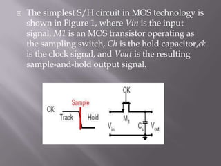
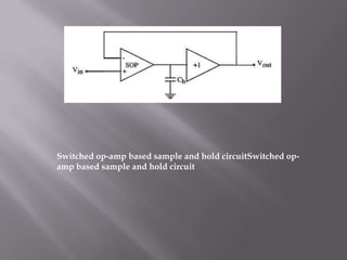

Sample-and-hold (S/H) circuits are important analog building blocks that are used in applications like analog-to-digital converters and switched-capacitor filters. The simplest S/H circuit uses an MOS transistor as a sampling switch and a hold capacitor. Switched op-amp based S/H circuits reduce errors from charge injection and clock feedthrough. S/H circuits are used to hold input signals constant for comparisons in circuits like successive approximation ADCs and to simultaneously sample multiple signals.


