Downloaded 521 times
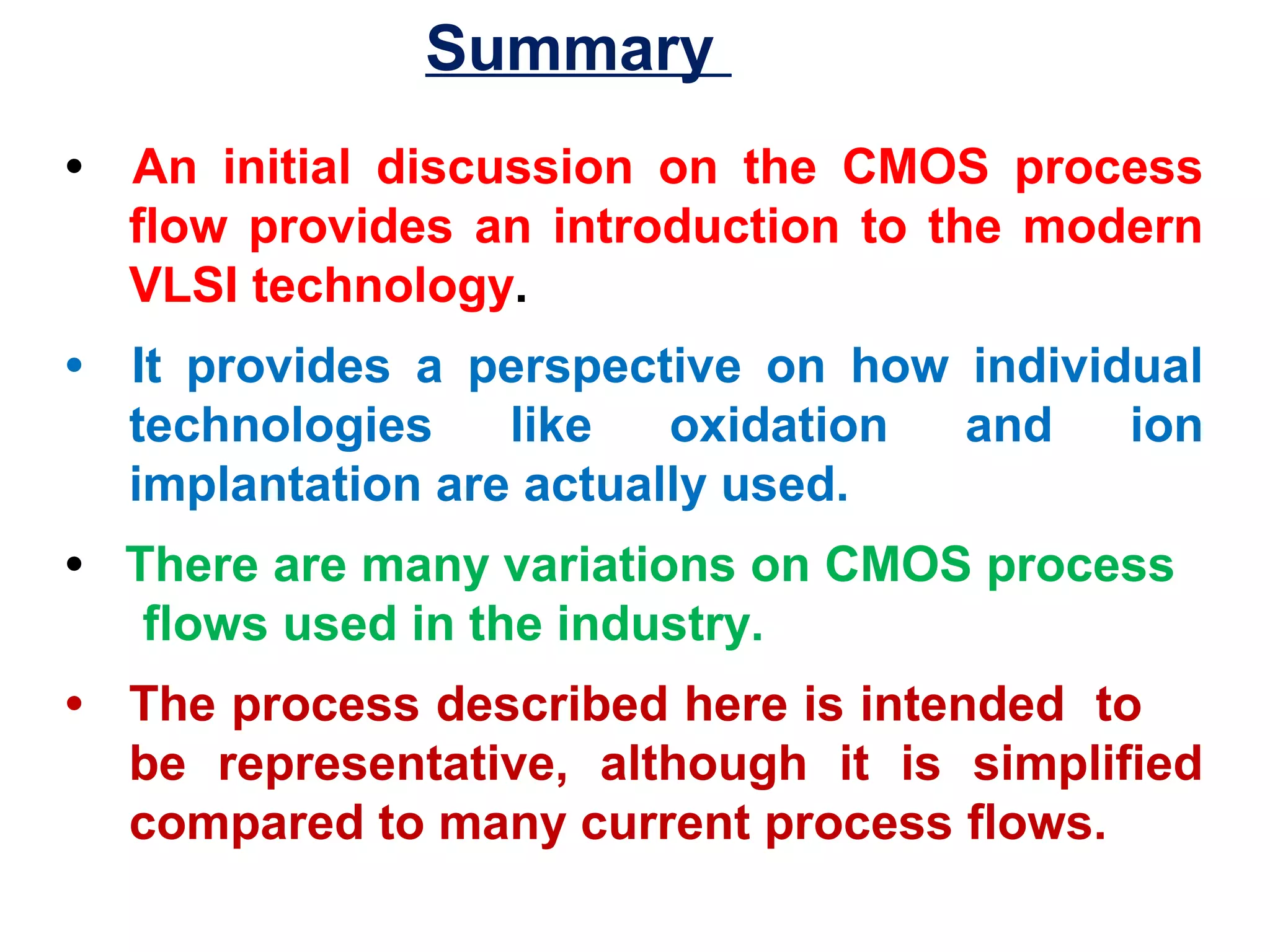


This document describes the key process steps in a standard CMOS fabrication process flow. It begins with an overview of basic CMOS circuits and substrate preparation. Then each major step is outlined, including well formation through ion implantation, gate oxide growth, polysilicon deposition and patterning, source/drain implantation and annealing. Additional metal layers are deposited and patterned before passivation completes the CMOS structure. The process requires 16 photomasks and over 100 individual process steps to fabricate modern integrated circuits using complementary NMOS and PMOS transistors.
Introduction to VLSI Fabrication Technology and overview of CMOS Technology.
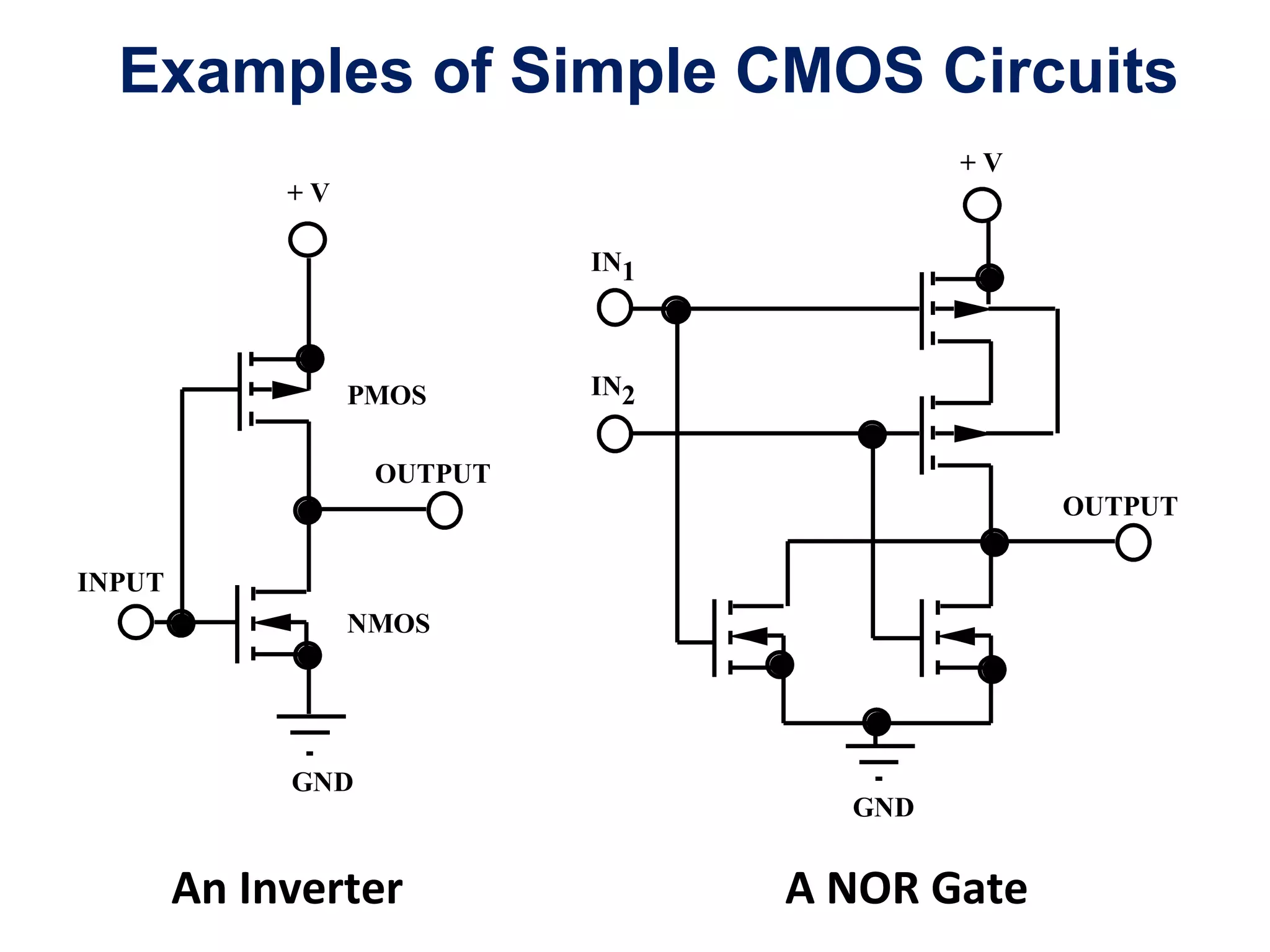
Illustration of simple CMOS circuits: an inverter and a NOR gate.
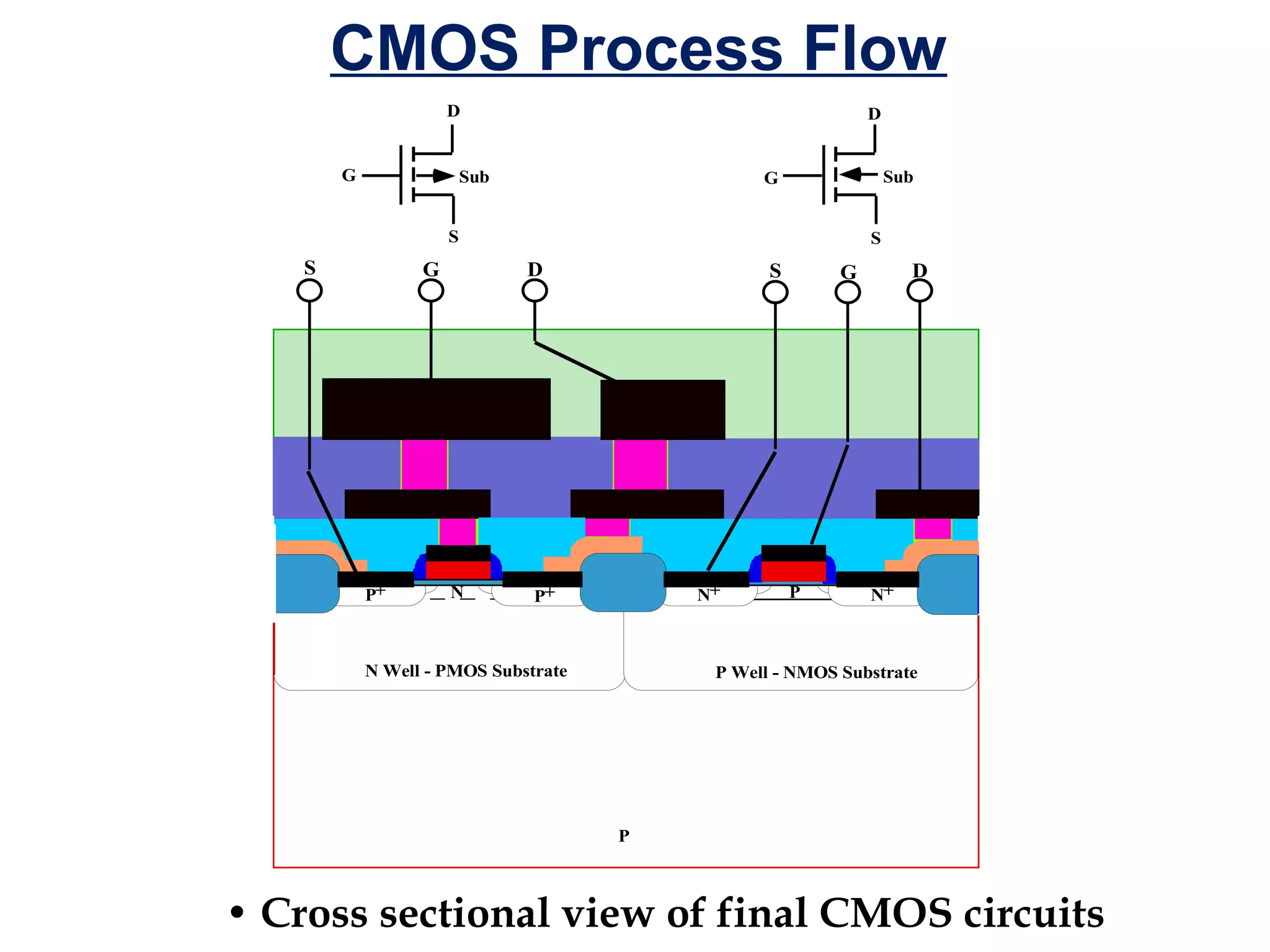
Cross-sectional view of final CMOS circuits indicating NMOS and PMOS substrates.
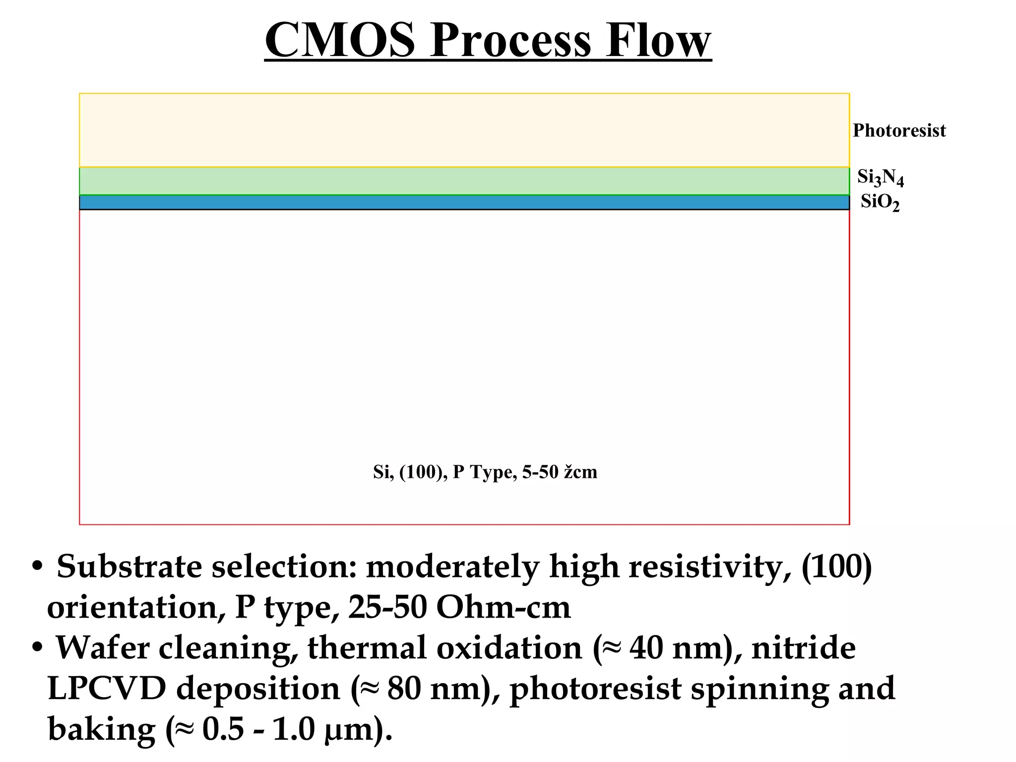
Details of substrate selection (P-type, resistivity, orientation) and the initial cleaning stages.
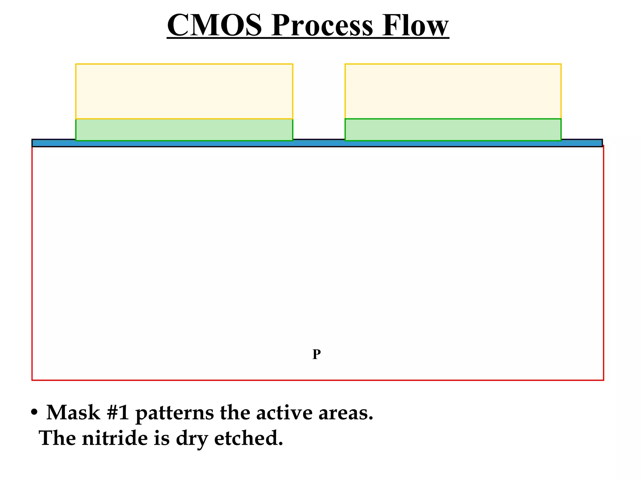
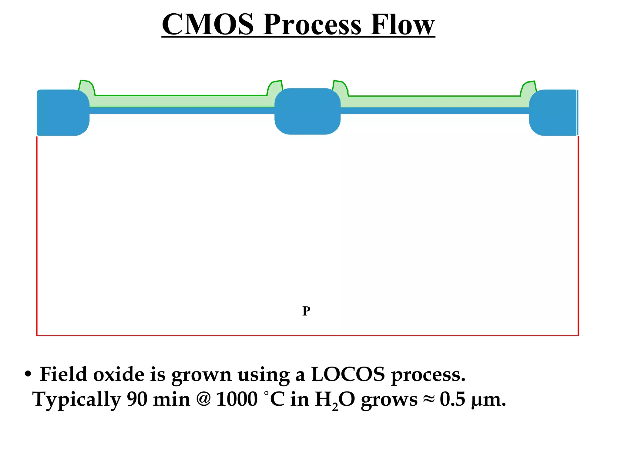
Patterning active areas and the growth of field oxide using LOCOS process.
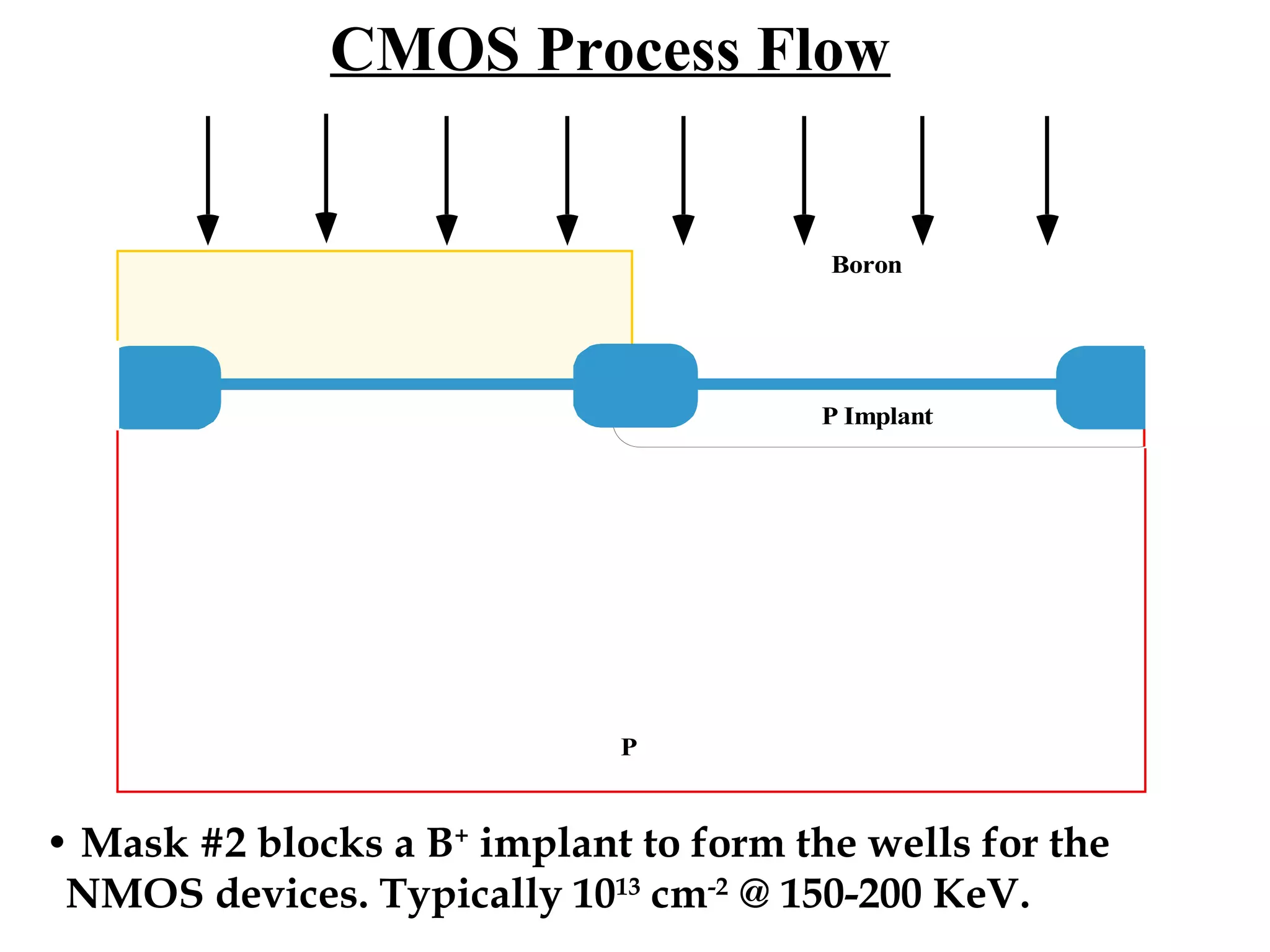
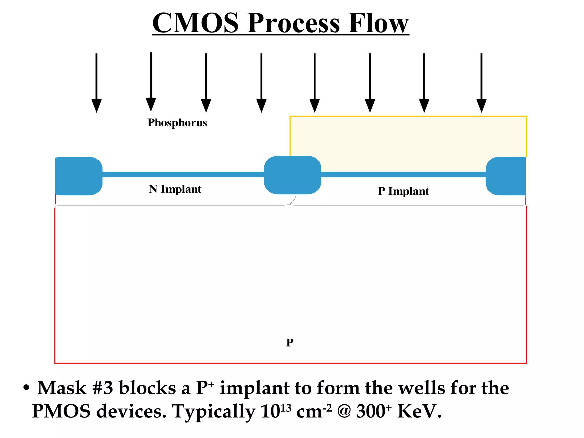
Description of implant processes for NMOS and PMOS device wells.
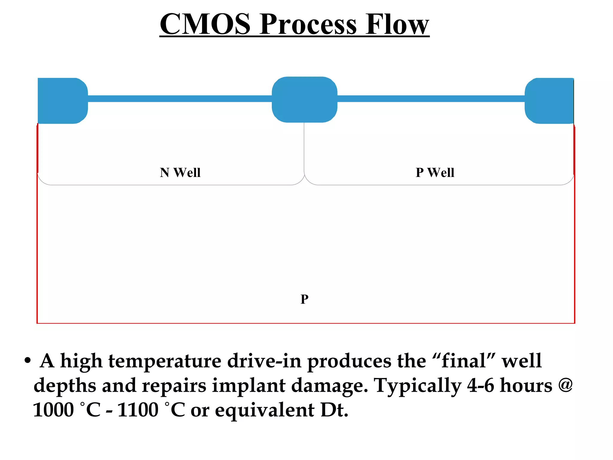
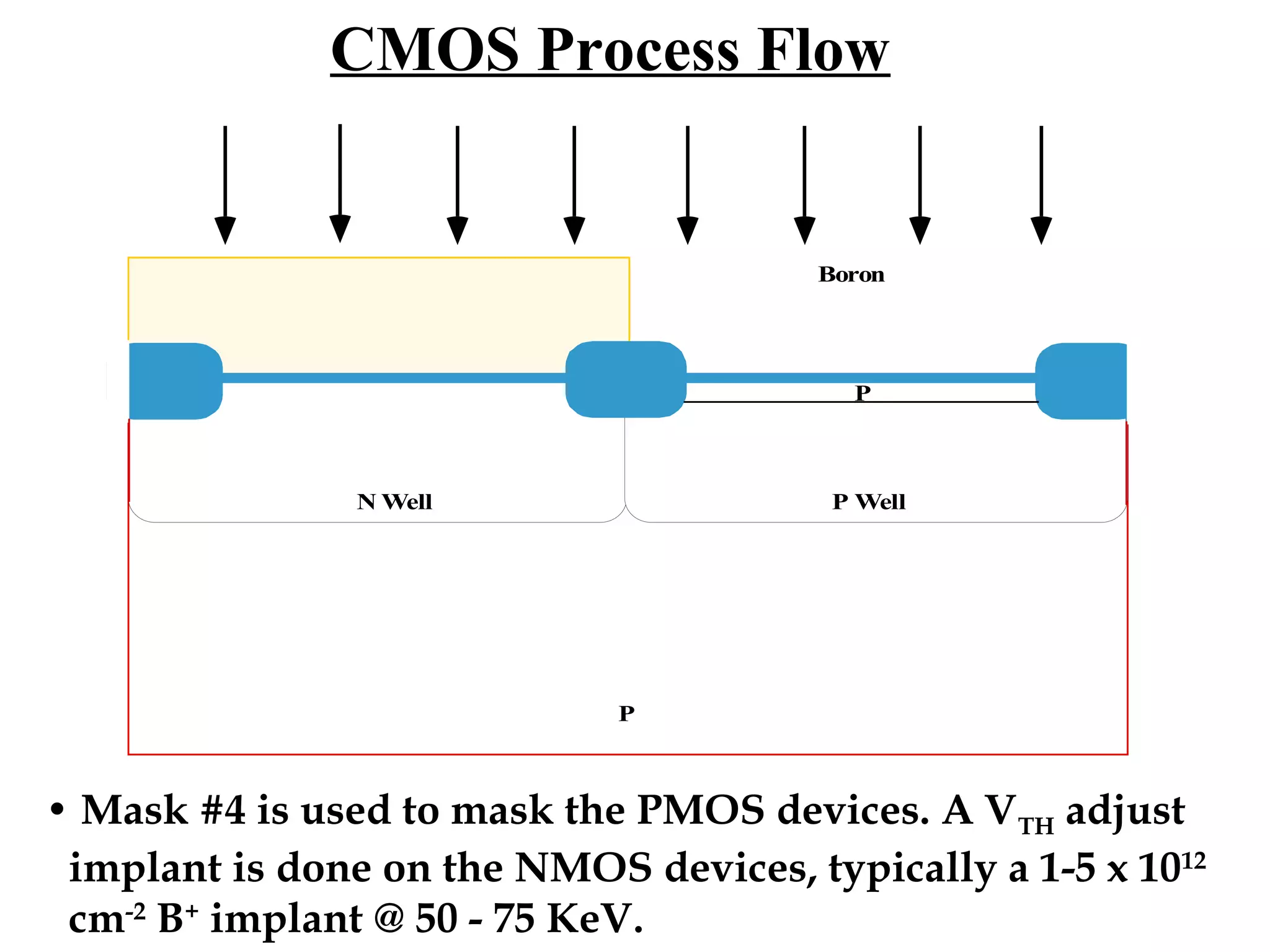
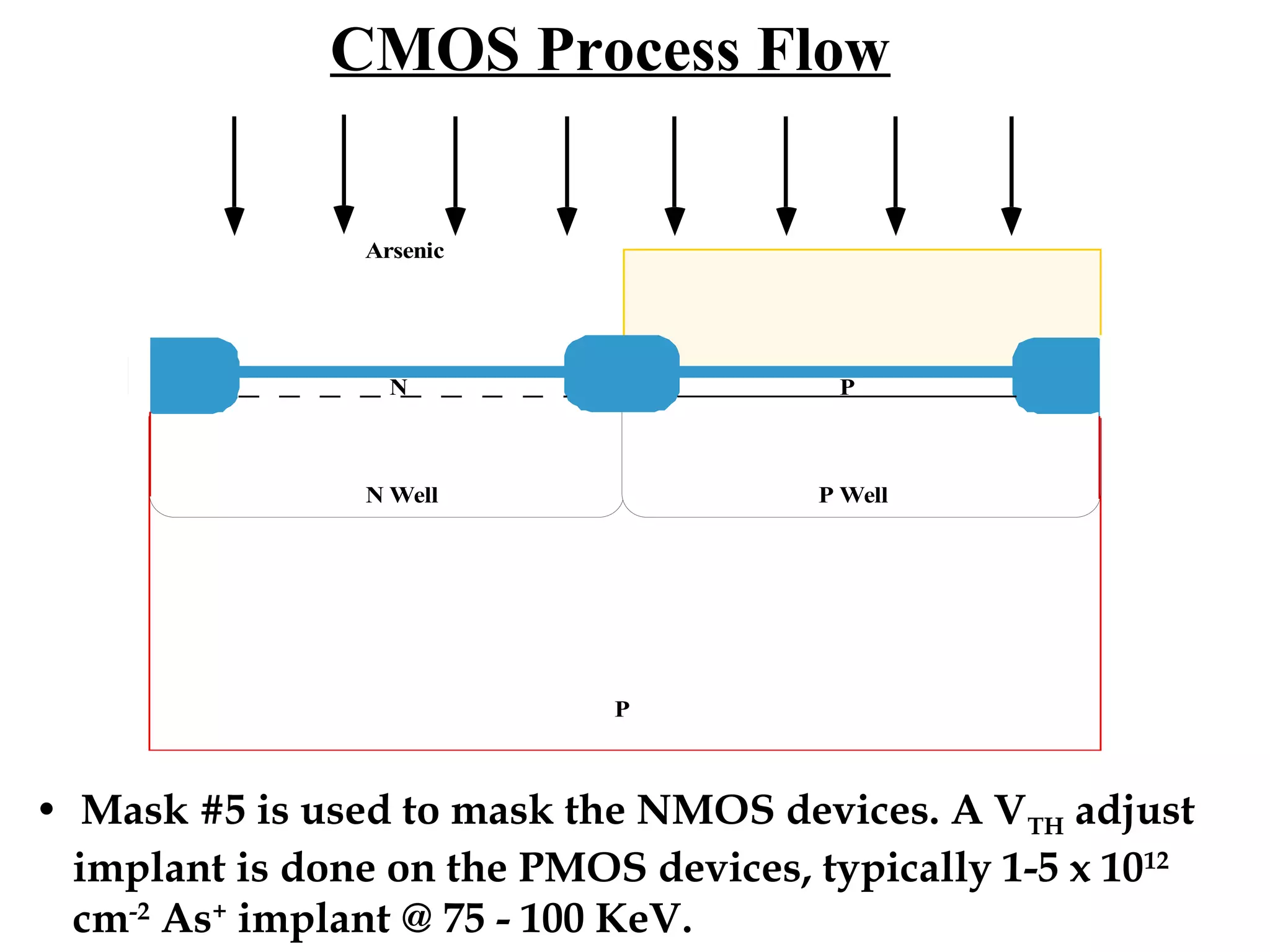
Discussion on well depths achieved through high temperature drive-in and VTH adjustments.
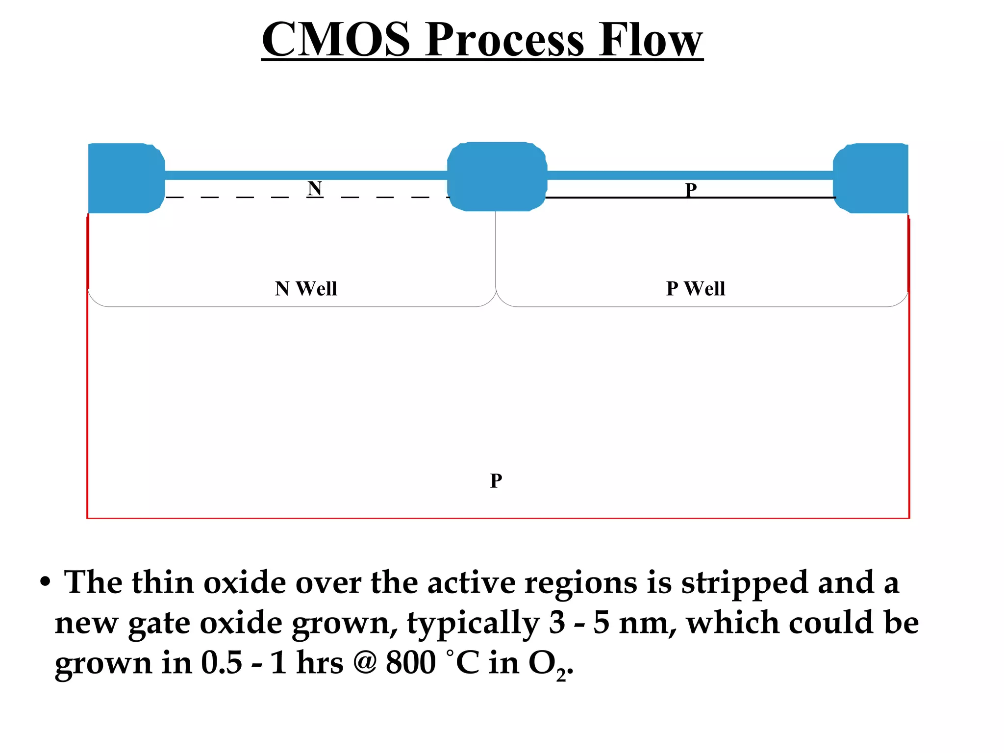
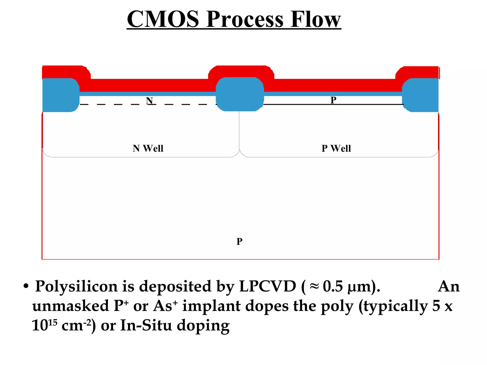
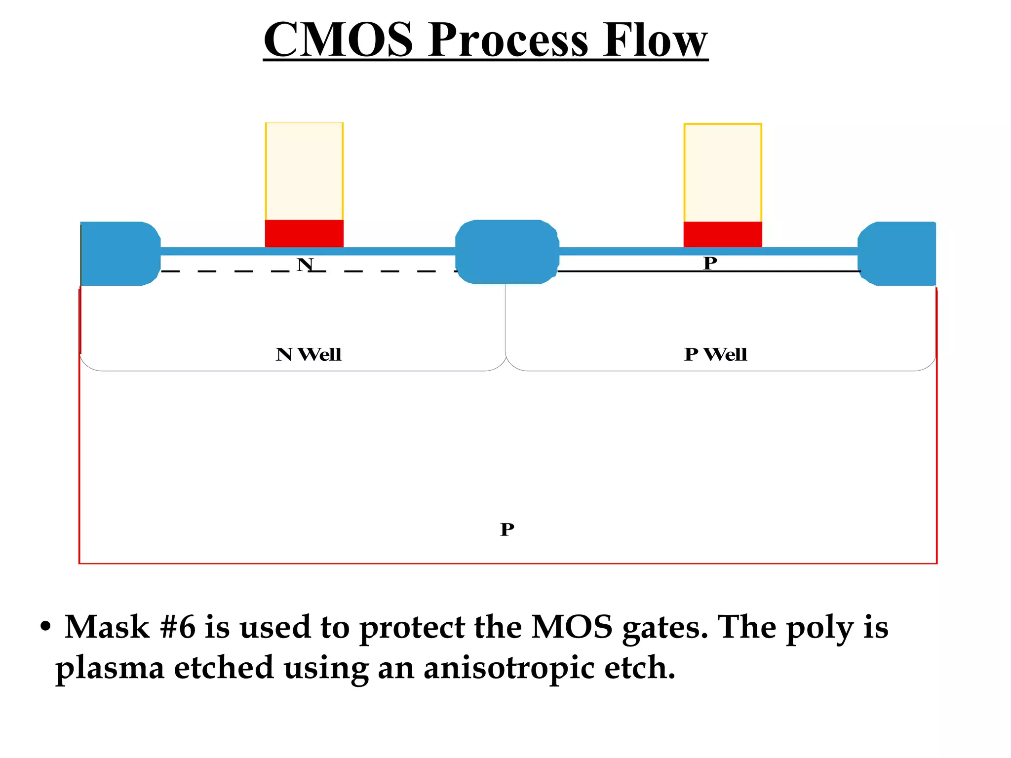
Processing of gate oxide stripping, polysilicon deposition, and doping of the polysilicon layer.
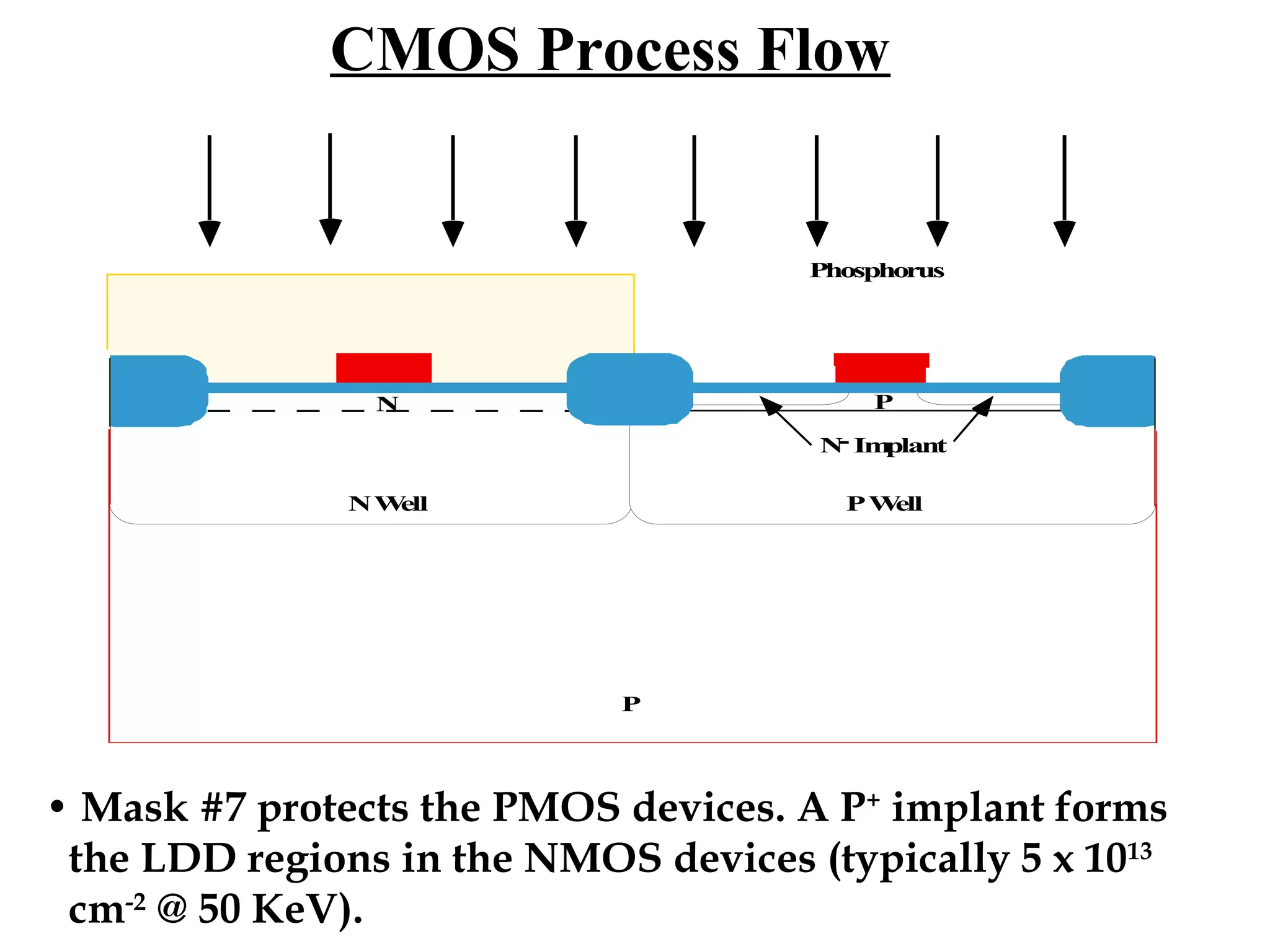
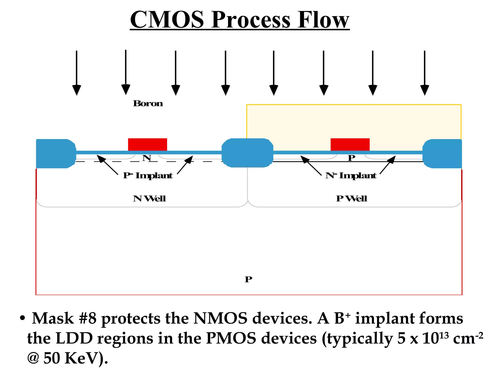
Details on masking protection and formation of LDD regions for NMOS and PMOS devices.
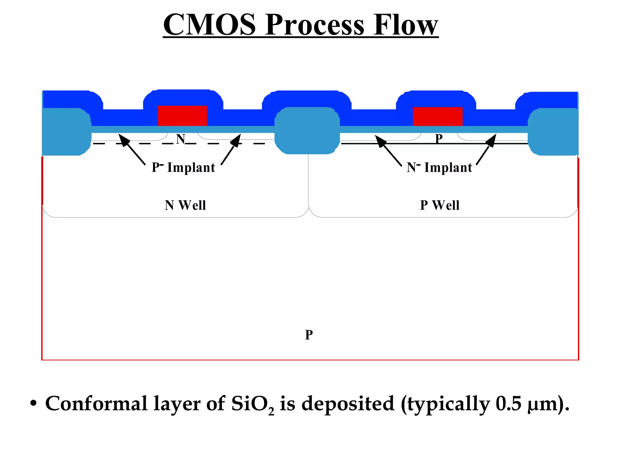
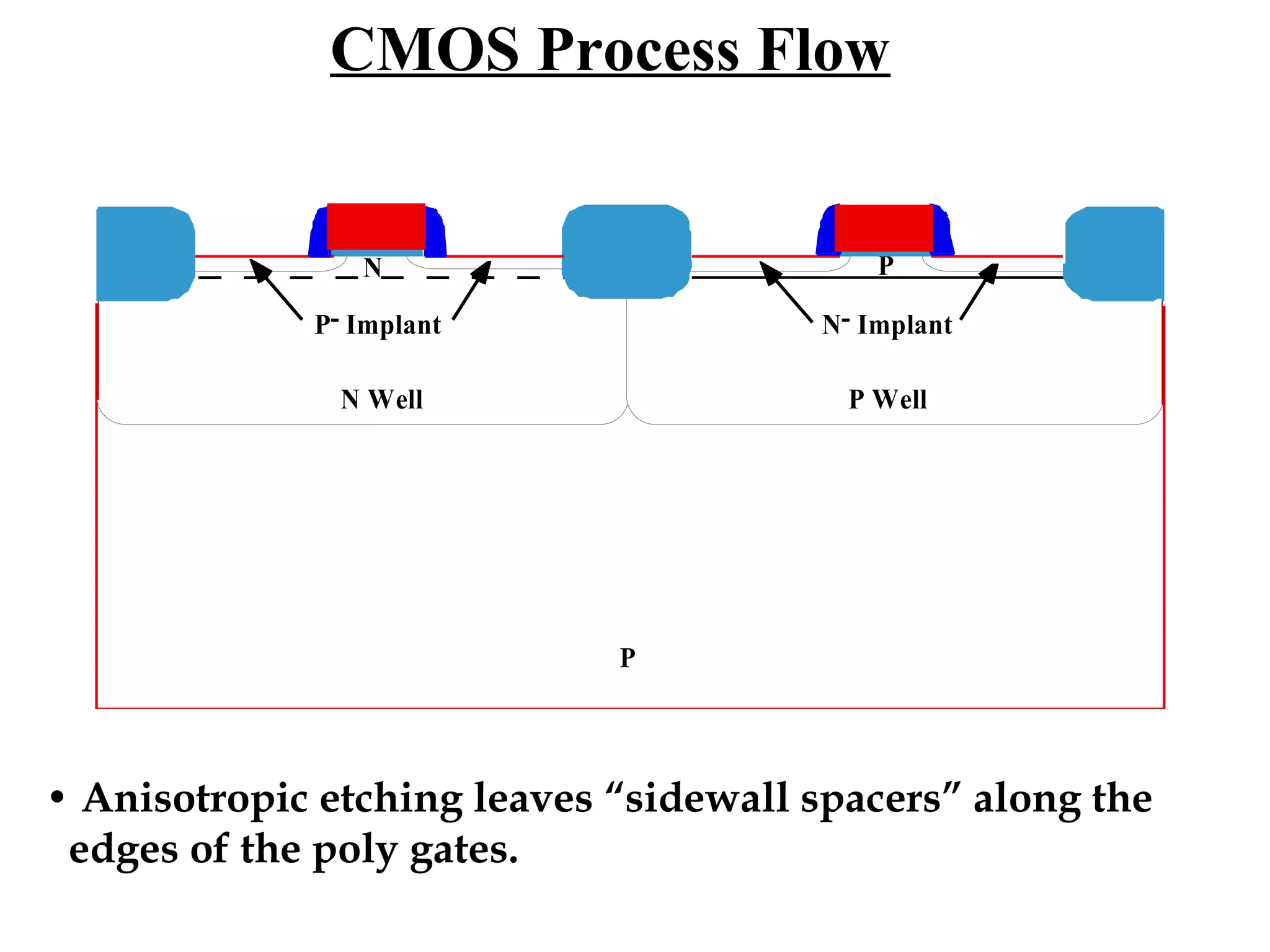
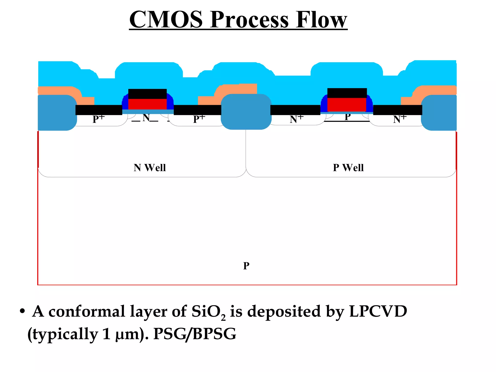
Deposition of conformal SiO2 layer and the process of anisotropic etching for sidewall spacers.
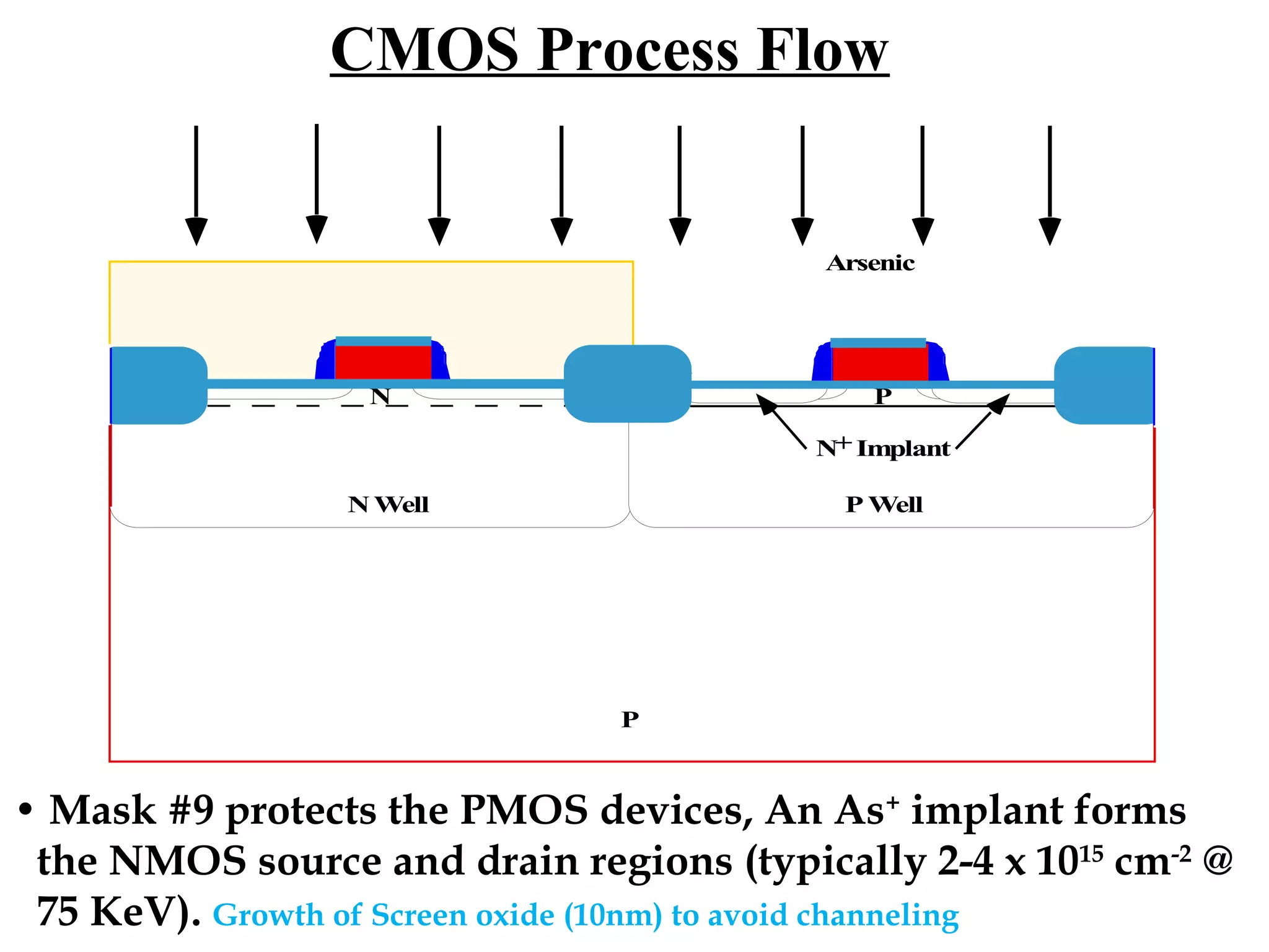
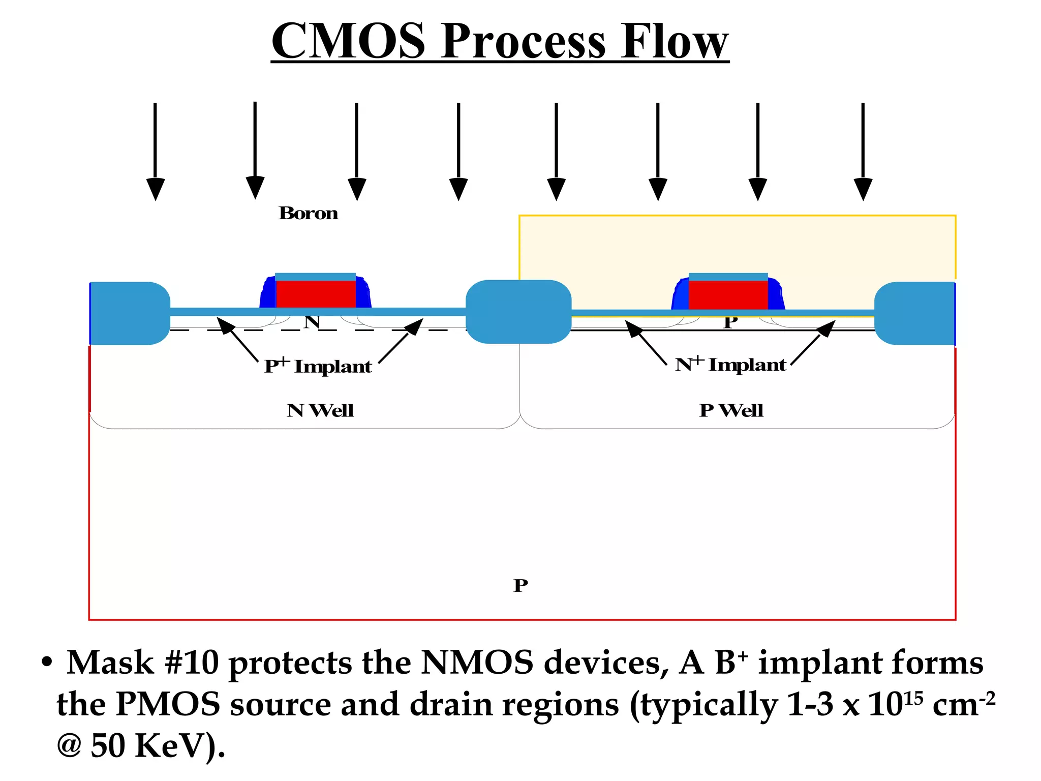
Formation of source and drain regions in NMOS and PMOS devices through As+ and B+ implants.
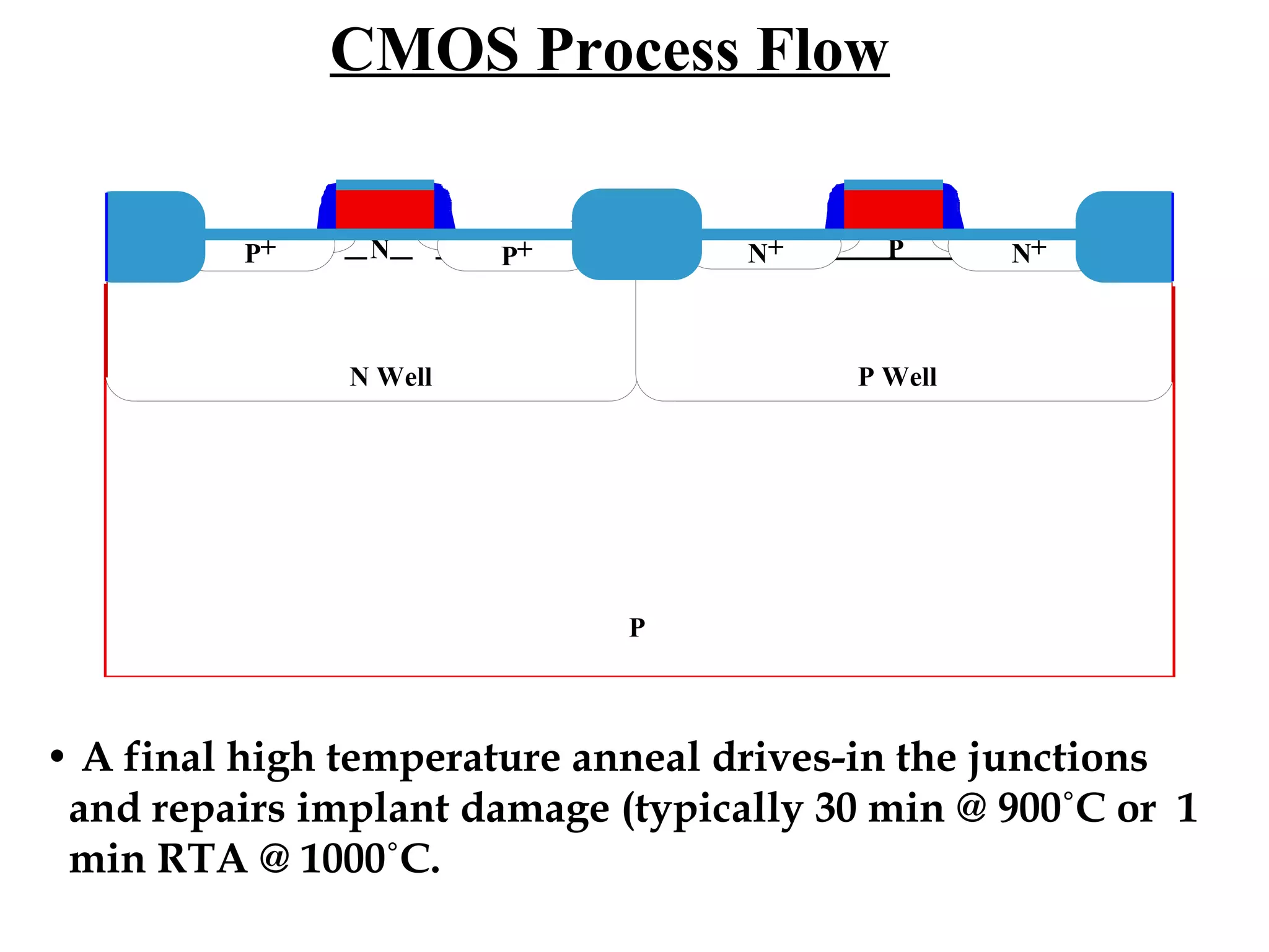
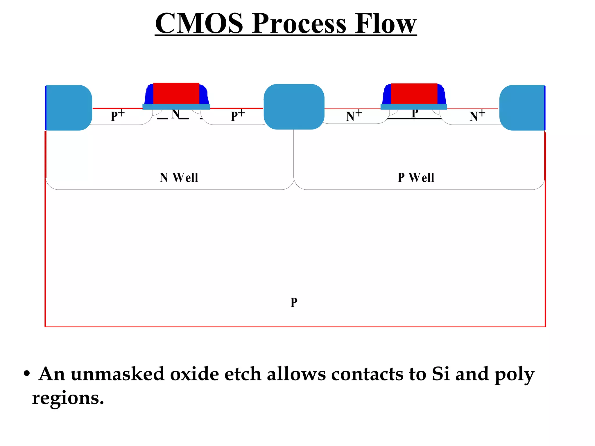
Final high-temperature anneal for junction drive-in and unmasked oxide etching.
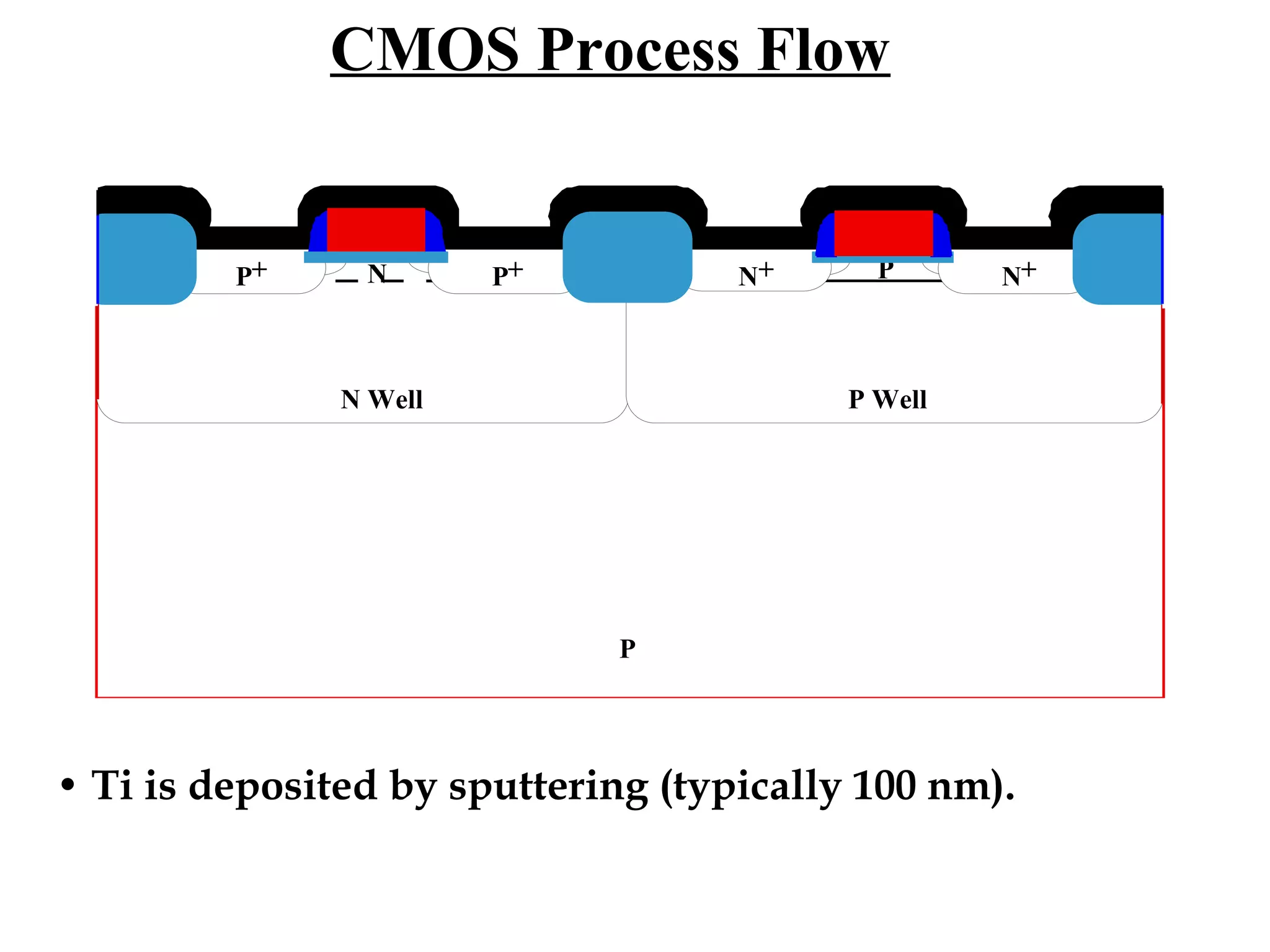
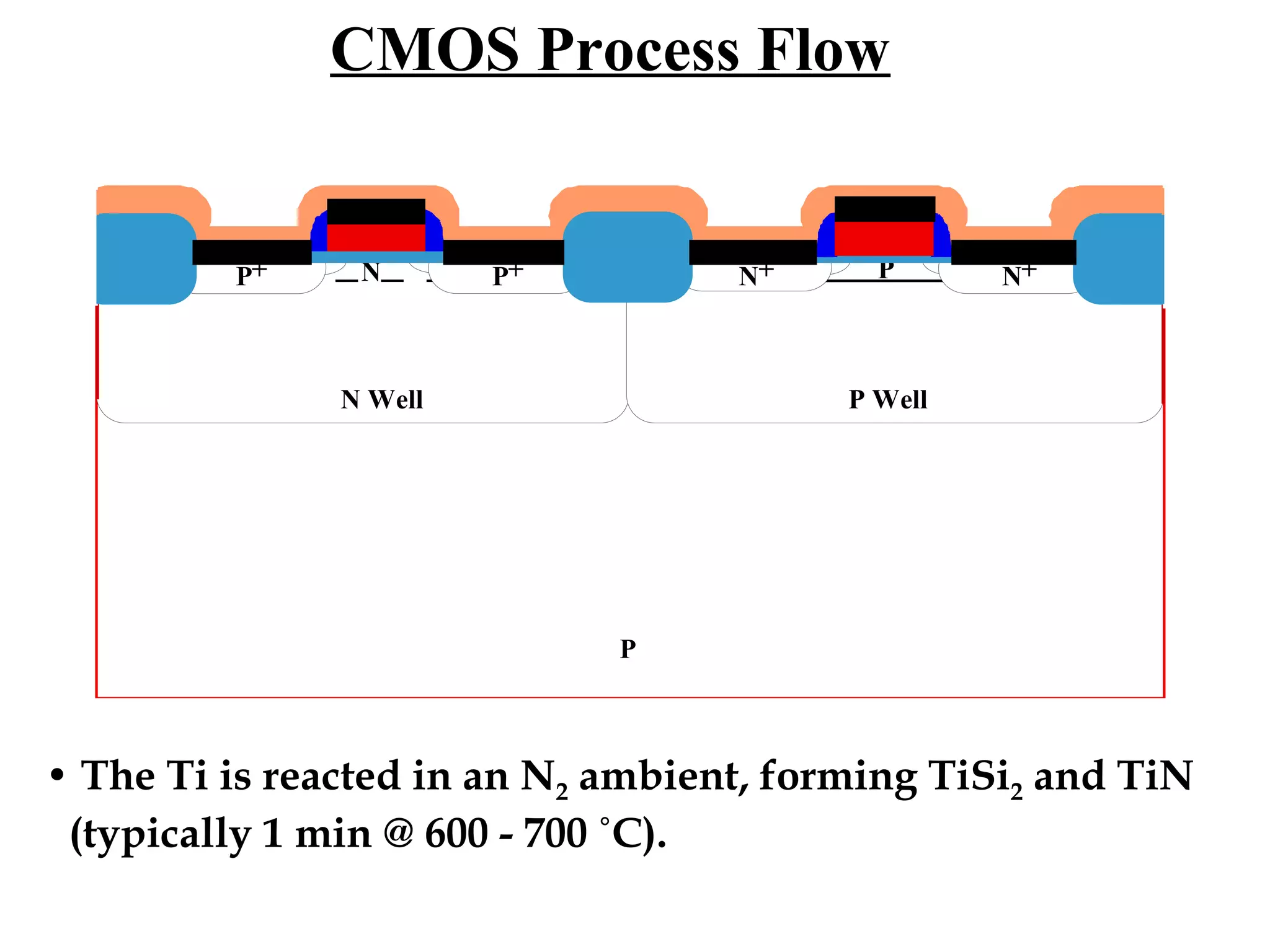
Sputtering and reaction of Ti layer to form conductive interconnects.
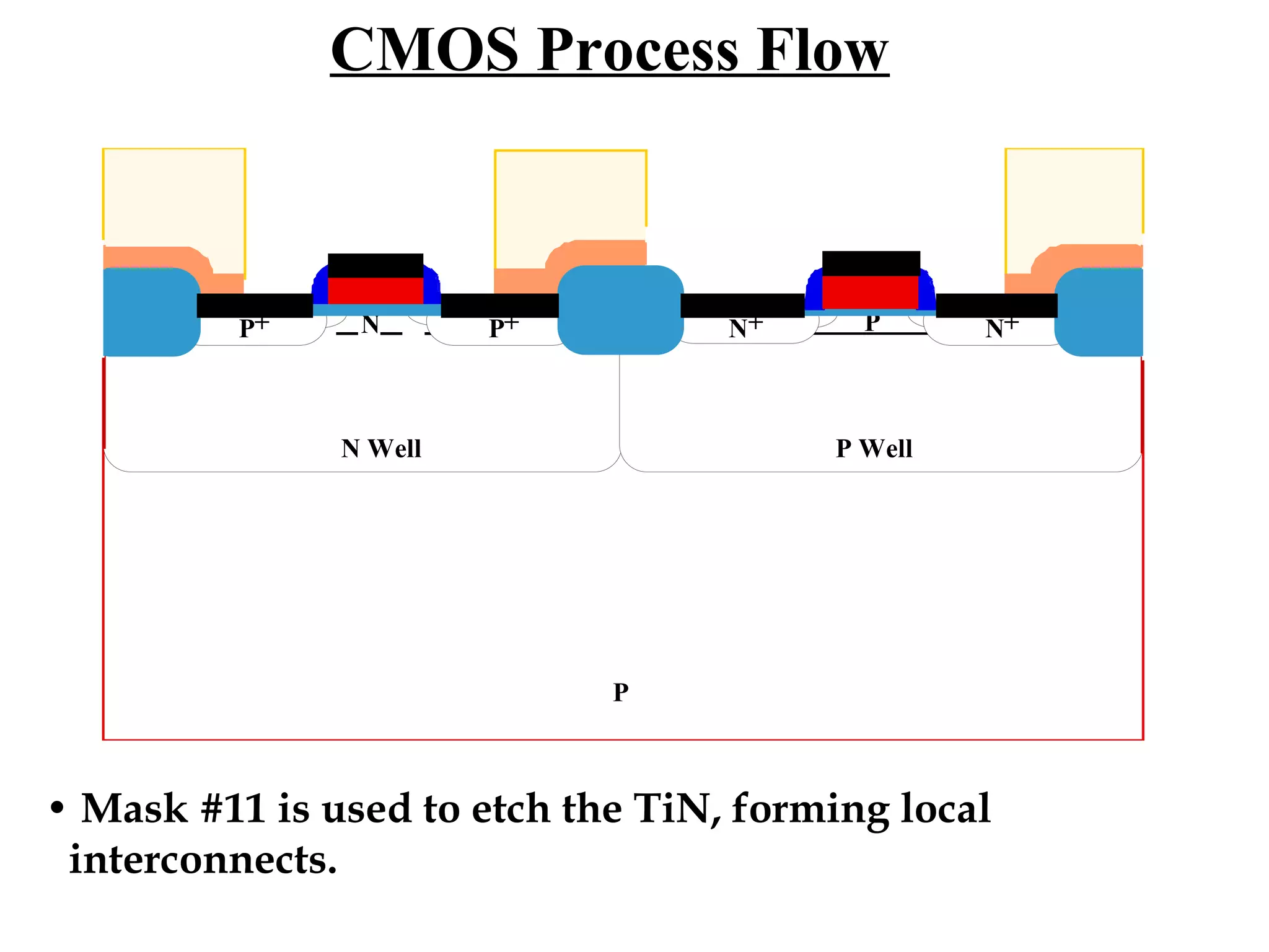
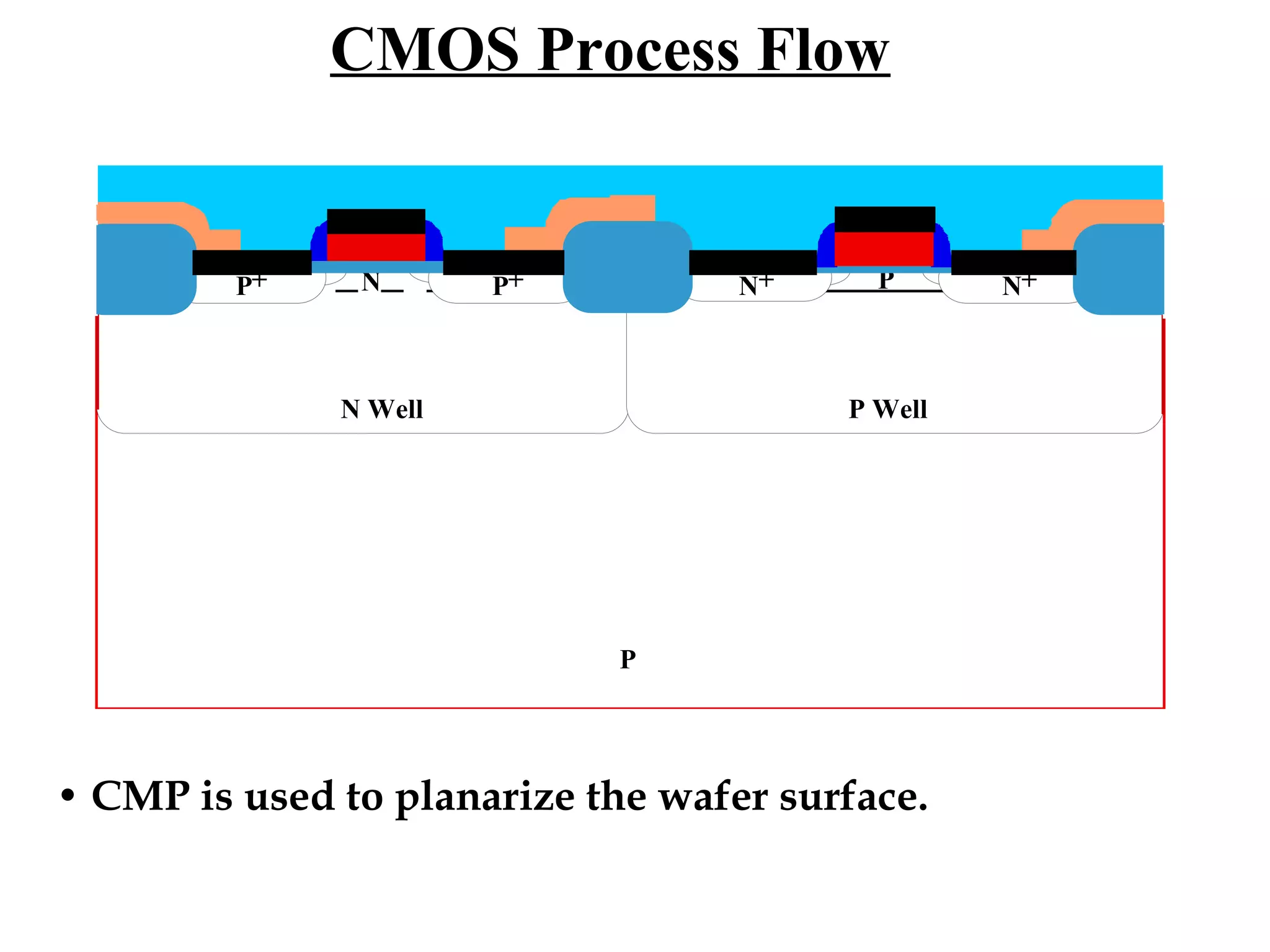
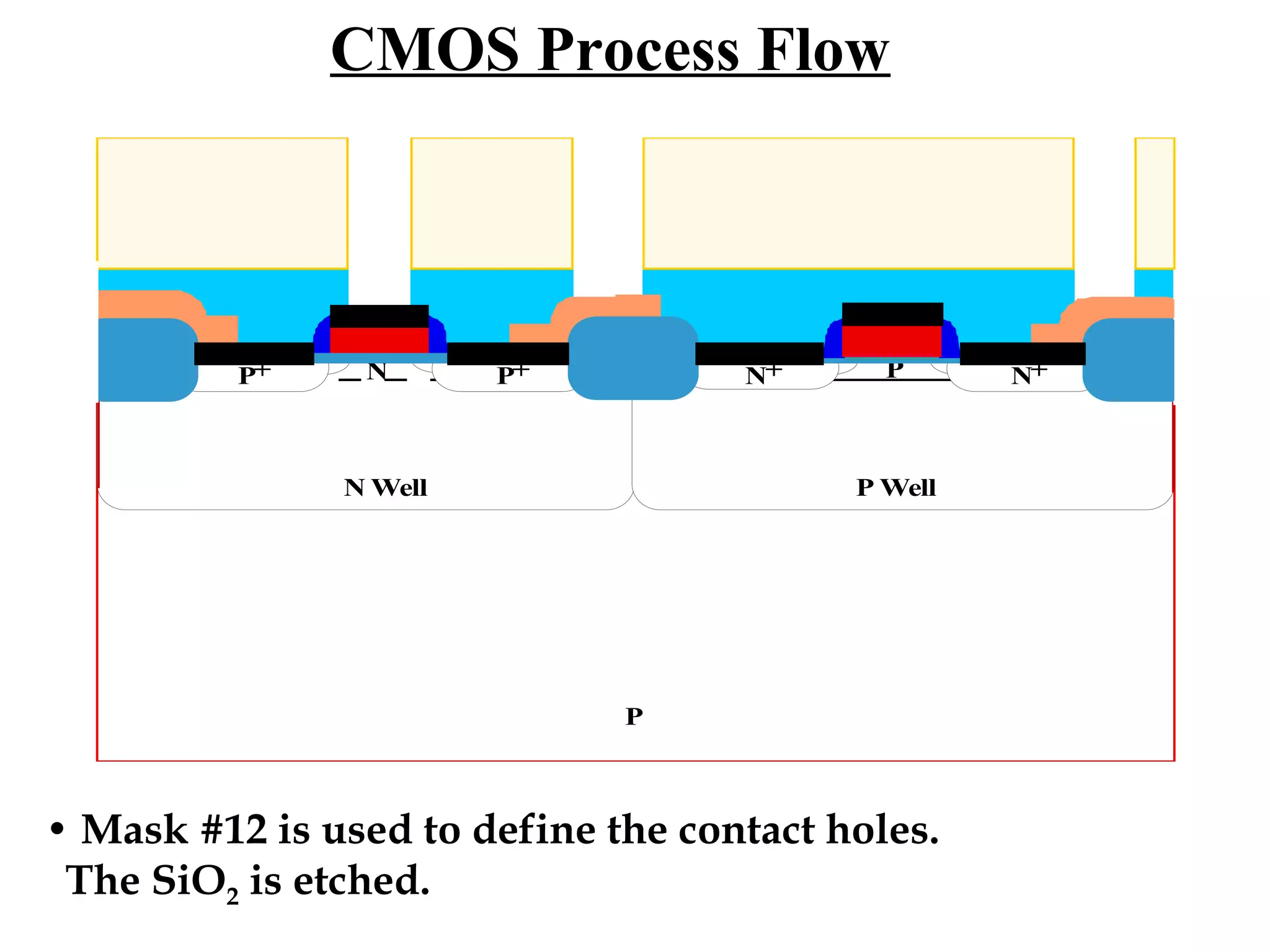
Defining contact holes and further etching processes for finalizing structure.
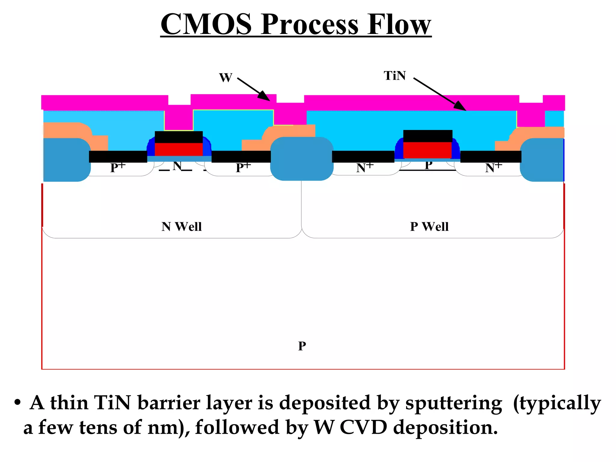
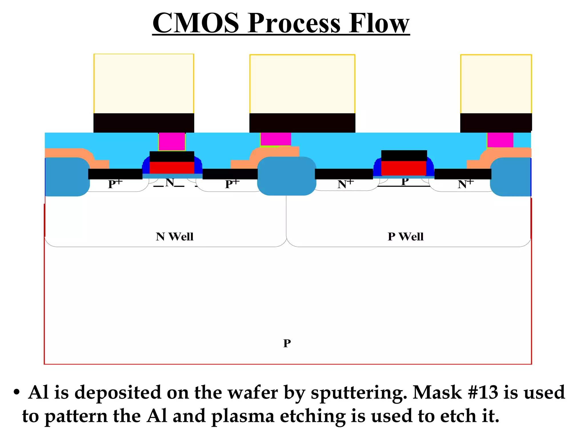
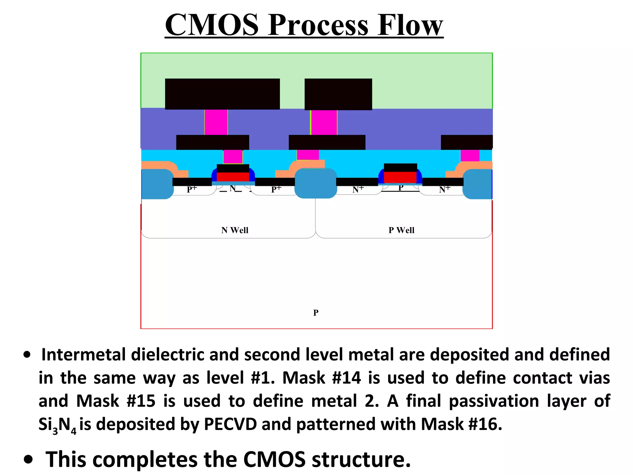
Finalizing CMOS structure through deposition of TiN, aluminum, and passivation layers.
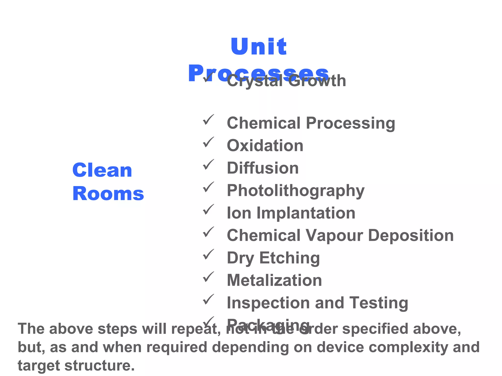
Overview of essential CMOS unit processes including crystal growth, photolithography, and others.
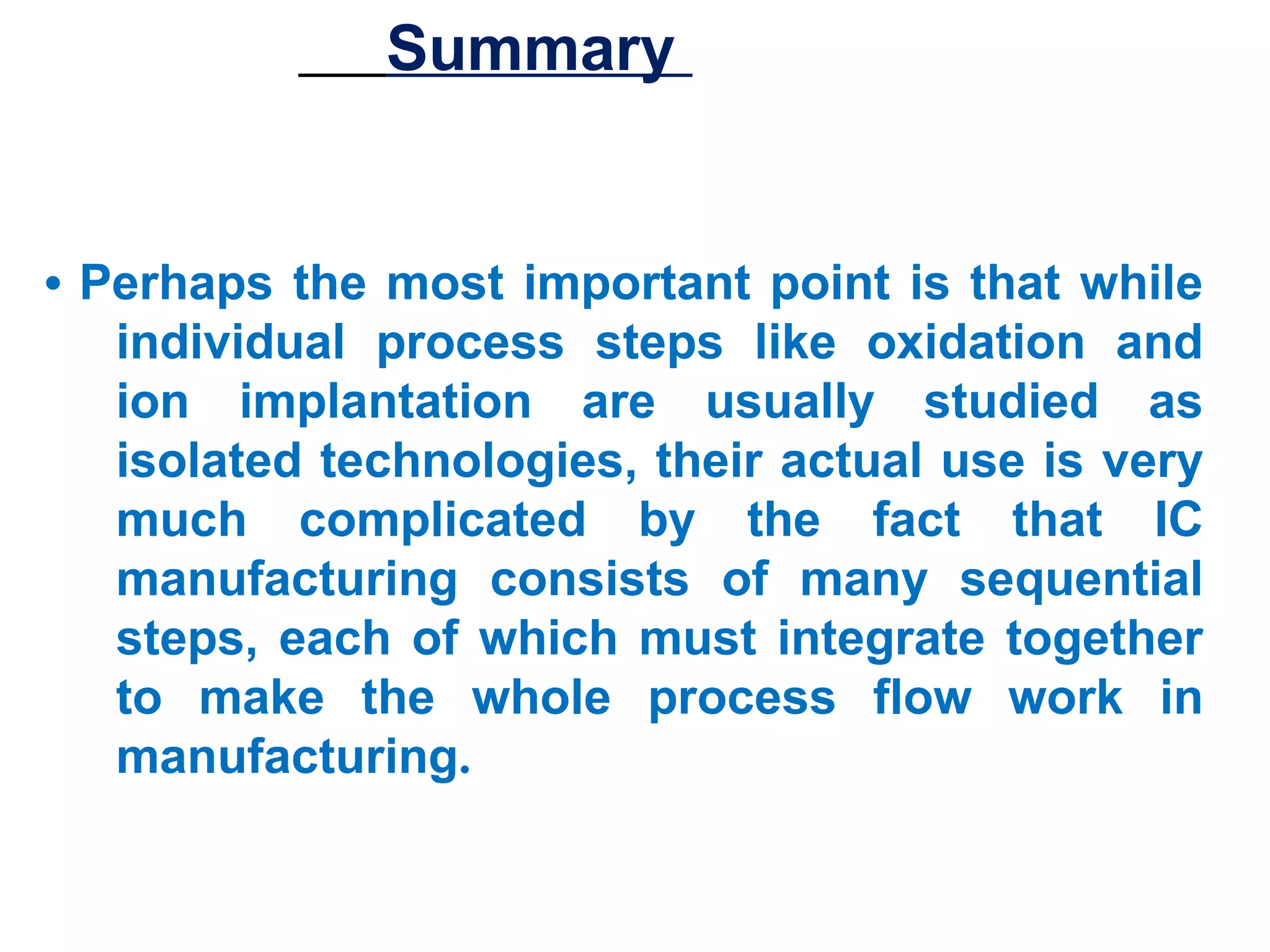
Introduction to different variations in CMOS flow, emphasizing integration of process technologies.
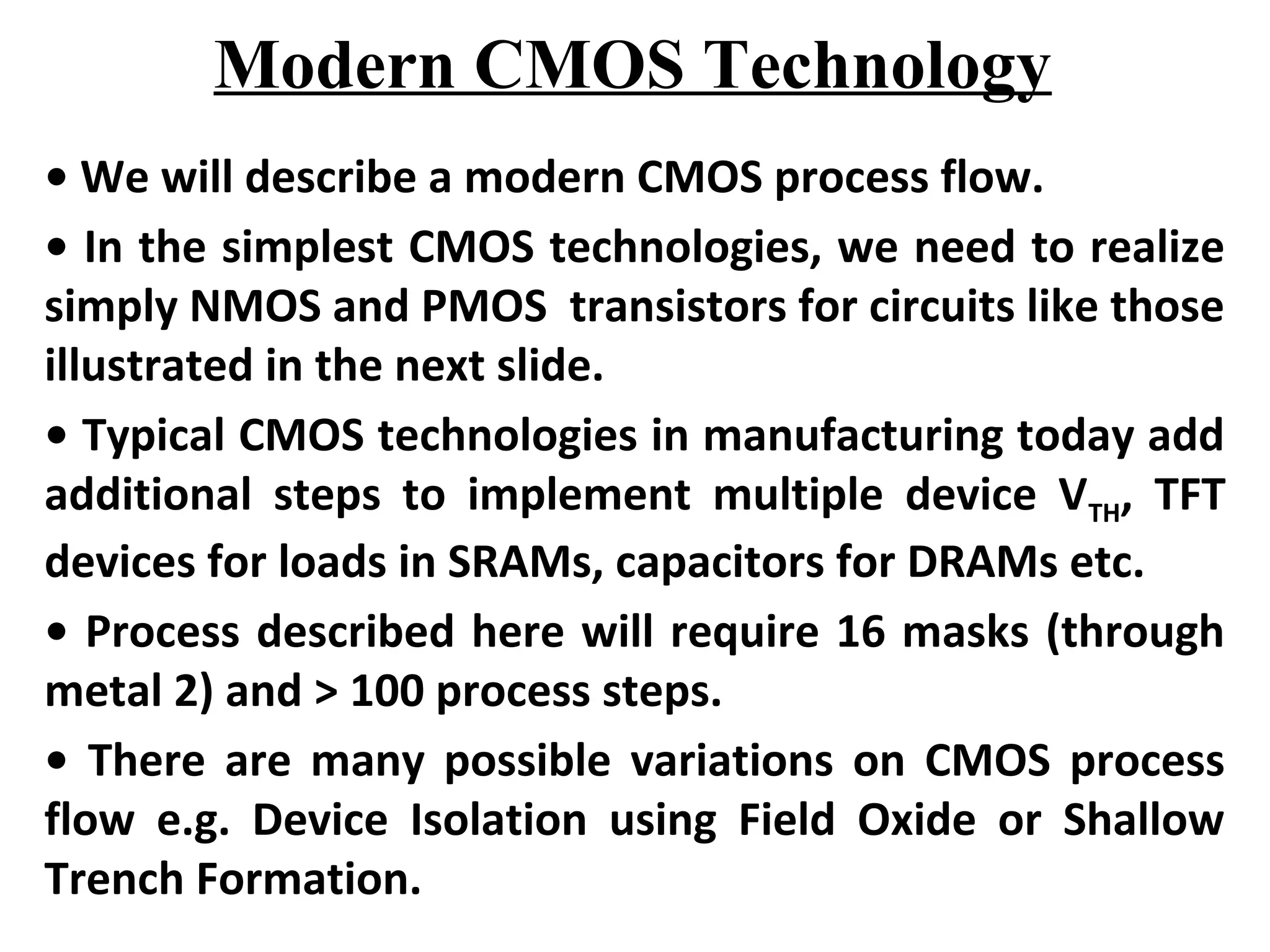
Description of modern CMOS process flow requiring multiple steps, masks, and variations.


