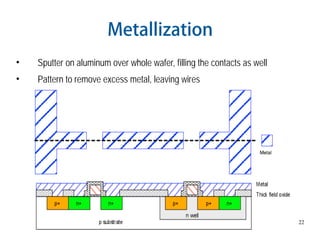
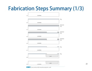
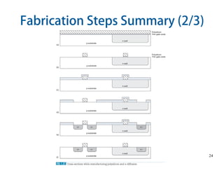
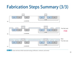
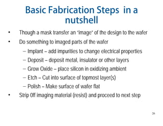
The document describes the process for fabricating CMOS transistors on a silicon wafer. Key steps include:
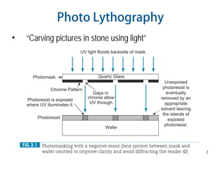
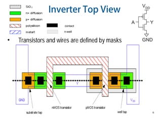
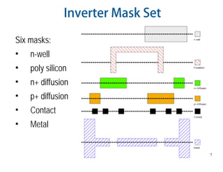
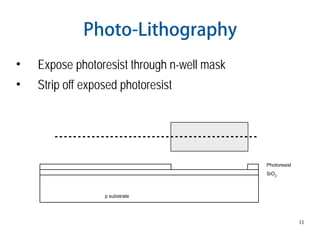
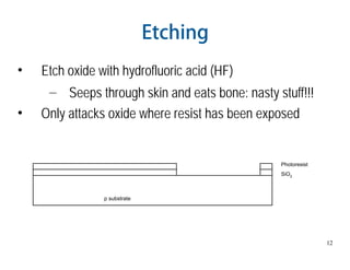
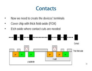
1. Depositing materials and etching layers through photolithography to define transistors, wells, and wiring layers on the wafer.
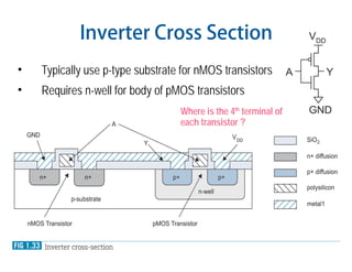
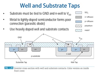
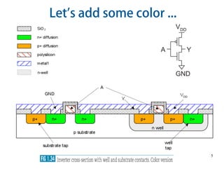
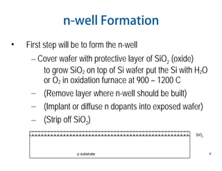
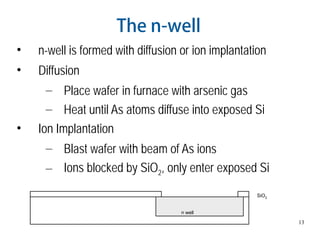
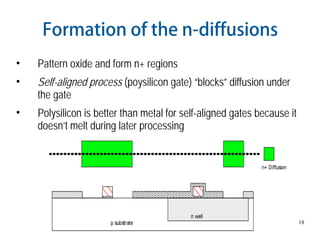
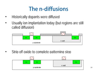
2. Forming the n-well and p-substrate regions through diffusion or implantation of dopants exposed by photomasks.
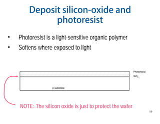
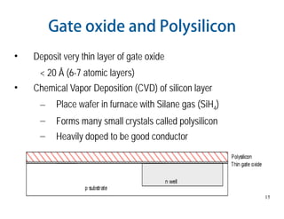
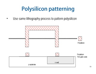
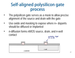
3. Depositing additional layers like gate oxide and polysilicon to define the transistor gates through further photolithography and etching steps.