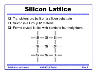
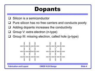
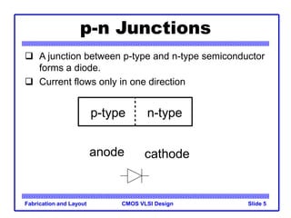
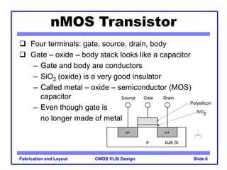
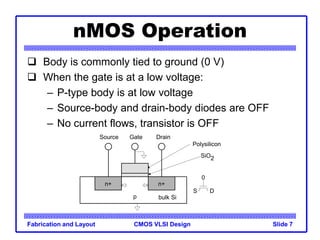
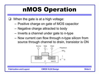
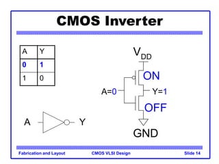
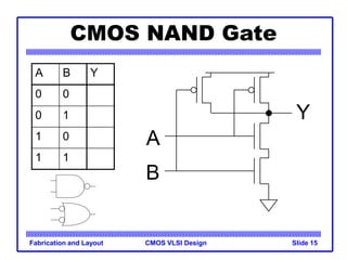
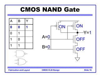
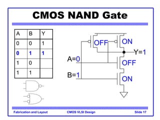
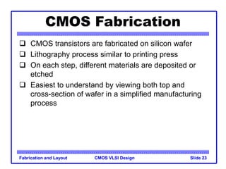
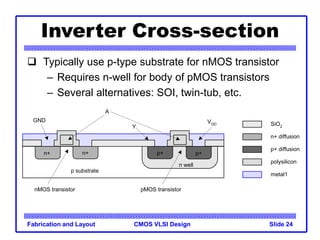
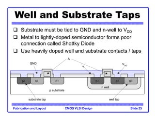
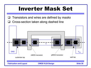
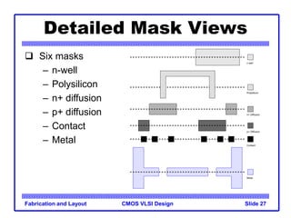
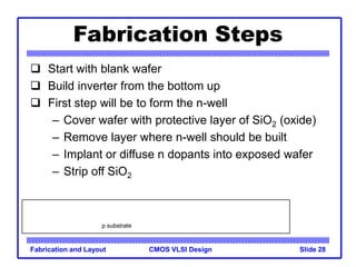
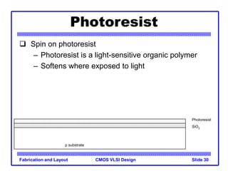
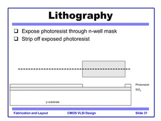
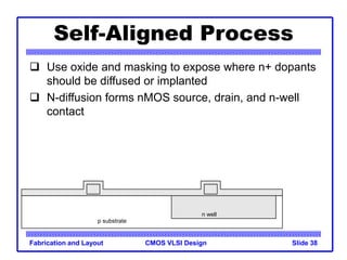
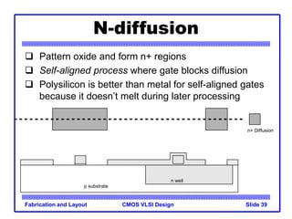
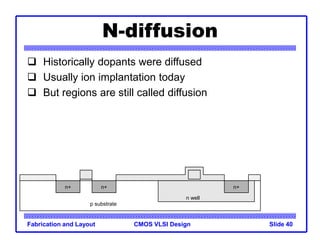
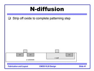
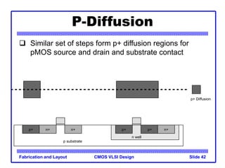
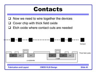
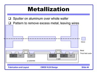
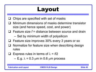
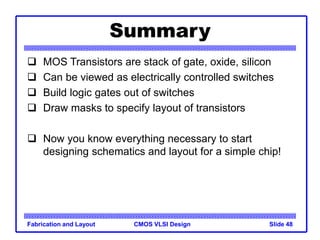
SlideShare a Scribd company logo
Introduction to
CMOS VLSI
Design
Layout, Fabrication, and
Elementary Logic Design
CMOS VLSI Design
Fabrication and Layout Slide 2
Introduction
 Integrated circuits: many transistors on one chip.
– Very Large Scale Integration (VLSI): very many
 Metal Oxide Semiconductor (MOS) transistor
– Fast, cheap, low-power transistors
– Complementary: mixture of n- and p-type leads to
less power
 Today: How to build your own simple CMOS chip
– CMOS transistors
– Building logic gates from transistors
– Transistor layout and fabrication
 Rest of the course: How to build a good CMOS chip
CMOS VLSI Design
Fabrication and Layout Slide 3
Silicon Lattice
 Transistors are built on a silicon substrate
 Silicon is a Group IV material
 Forms crystal lattice with bonds to four neighbors
Si Si
Si
Si Si
Si
Si Si
Si
CMOS VLSI Design
Fabrication and Layout Slide 4
Dopants
 Silicon is a semiconductor
 Pure silicon has no free carriers and conducts poorly
 Adding dopants increases the conductivity
 Group V: extra electron (n-type)
 Group III: missing electron, called hole (p-type)
As Si
Si
Si Si
Si
Si Si
Si
B Si
Si
Si Si
Si
Si Si
Si
-
+
+
-
CMOS VLSI Design
Fabrication and Layout Slide 5
p-n Junctions
 A junction between p-type and n-type semiconductor
forms a diode.
 Current flows only in one direction
p-type n-type
anode cathode
CMOS VLSI Design
Fabrication and Layout Slide 6
nMOS Transistor
 Four terminals: gate, source, drain, body
 Gate – oxide – body stack looks like a capacitor
– Gate and body are conductors
– SiO2 (oxide) is a very good insulator
– Called metal – oxide – semiconductor (MOS)
capacitor
– Even though gate is
no longer made of metal
n+
p
Gate
Source Drain
bulk Si
SiO2
Polysilicon
n+
CMOS VLSI Design
Fabrication and Layout Slide 7
nMOS Operation
 Body is commonly tied to ground (0 V)
 When the gate is at a low voltage:
– P-type body is at low voltage
– Source-body and drain-body diodes are OFF
– No current flows, transistor is OFF
n+
p
Gate
Source Drain
bulk Si
SiO2
Polysilicon
n+
D
0
S
CMOS VLSI Design
Fabrication and Layout Slide 8
nMOS Operation
 When the gate is at a high voltage:
– Positive charge on gate of MOS capacitor
– Negative charge attracted to body
– Inverts a channel under gate to n-type
– Now current can flow through n-type silicon from
source through channel to drain, transistor is ON
n+
p
Gate
Source Drain
bulk Si
SiO2
Polysilicon
n+
D
1
S
CMOS VLSI Design
Fabrication and Layout Slide 9
pMOS Transistor
 Similar, but doping and voltages reversed
– Body tied to high voltage (VDD)
– Gate low: transistor ON
– Gate high: transistor OFF
– Bubble indicates inverted behavior
SiO2
n
Gate
Source Drain
bulk Si
Polysilicon
p+ p+
CMOS VLSI Design
Fabrication and Layout Slide 10
Power Supply Voltage
 GND = 0 V
 In 1980’s, VDD = 5V
 VDD has decreased in modern processes
– High VDD would damage modern tiny transistors
– Lower VDD saves power
 VDD = 3.3, 2.5, 1.8, 1.5, 1.2, 1.0, …
CMOS VLSI Design
Fabrication and Layout Slide 11
Transistors as Switches
 We can view MOS transistors as electrically
controlled switches
 Voltage at gate controls path from source to drain
g
s
d
g = 0
s
d
g = 1
s
d
g
s
d
s
d
s
d
nMOS
pMOS
OFF
ON
ON
OFF
CMOS VLSI Design
Fabrication and Layout Slide 12
CMOS Inverter
A Y
0
1
VDD
A Y
GND
A Y
CMOS VLSI Design
Fabrication and Layout Slide 13
CMOS Inverter
A Y
0
1 0
VDD
A=1 Y=0
GND
ON
OFF
A Y
CMOS VLSI Design
Fabrication and Layout Slide 14
CMOS Inverter
A Y
0 1
1 0
VDD
A=0 Y=1
GND
OFF
ON
A Y
CMOS VLSI Design
Fabrication and Layout Slide 15
CMOS NAND Gate
A B Y
0 0
0 1
1 0
1 1
A
B
Y
CMOS VLSI Design
Fabrication and Layout Slide 16
CMOS NAND Gate
A B Y
0 0 1
0 1
1 0
1 1
A=0
B=0
Y=1
OFF
ON ON
OFF
CMOS VLSI Design
Fabrication and Layout Slide 17
CMOS NAND Gate
A B Y
0 0 1
0 1 1
1 0
1 1
A=0
B=1
Y=1
OFF
OFF ON
ON
CMOS VLSI Design
Fabrication and Layout Slide 18
CMOS NAND Gate
A B Y
0 0 1
0 1 1
1 0 1
1 1
A=1
B=0
Y=1
ON
ON OFF
OFF
CMOS VLSI Design
Fabrication and Layout Slide 19
CMOS NAND Gate
A B Y
0 0 1
0 1 1
1 0 1
1 1 0
A=1
B=1
Y=0
ON
OFF OFF
ON
CMOS VLSI Design
Fabrication and Layout Slide 20
CMOS NOR Gate
A B Y
0 0 1
0 1 0
1 0 0
1 1 0
A
B
Y
CMOS VLSI Design
Fabrication and Layout Slide 21
3-input NAND Gate
 Y pulls low if ALL inputs are 1
 Y pulls high if ANY input is 0
CMOS VLSI Design
Fabrication and Layout Slide 22
3-input NAND Gate
 Y pulls low if ALL inputs are 1
 Y pulls high if ANY input is 0
A
B
Y
C
CMOS VLSI Design
Fabrication and Layout Slide 23
CMOS Fabrication
 CMOS transistors are fabricated on silicon wafer
 Lithography process similar to printing press
 On each step, different materials are deposited or
etched
 Easiest to understand by viewing both top and
cross-section of wafer in a simplified manufacturing
process
CMOS VLSI Design
Fabrication and Layout Slide 24
Inverter Cross-section
 Typically use p-type substrate for nMOS transistor
– Requires n-well for body of pMOS transistors
– Several alternatives: SOI, twin-tub, etc.
n+
p substrate
p+
n well
A
Y
GND VDD
n+ p+
SiO2
n+ diffusion
p+ diffusion
polysilicon
metal1
nMOS transistor pMOS transistor
CMOS VLSI Design
Fabrication and Layout Slide 25
Well and Substrate Taps
 Substrate must be tied to GND and n-well to VDD
 Metal to lightly-doped semiconductor forms poor
connection called Shottky Diode
 Use heavily doped well and substrate contacts / taps
n+
p substrate
p+
n well
A
Y
GND VDD
n+
p+
substrate tap well tap
n+ p+
CMOS VLSI Design
Fabrication and Layout Slide 26
Inverter Mask Set
 Transistors and wires are defined by masks
 Cross-section taken along dashed line
GND VDD
Y
A
substrate tap well tap
nMOS transistor pMOS transistor
CMOS VLSI Design
Fabrication and Layout Slide 27
Detailed Mask Views
 Six masks
– n-well
– Polysilicon
– n+ diffusion
– p+ diffusion
– Contact
– Metal
Metal
Polysilicon
Contact
n+ Diffusion
p+ Diffusion
n well
CMOS VLSI Design
Fabrication and Layout Slide 28
Fabrication Steps
 Start with blank wafer
 Build inverter from the bottom up
 First step will be to form the n-well
– Cover wafer with protective layer of SiO2 (oxide)
– Remove layer where n-well should be built
– Implant or diffuse n dopants into exposed wafer
– Strip off SiO2
p substrate
CMOS VLSI Design
Fabrication and Layout Slide 29
Oxidation
 Grow SiO2 on top of Si wafer
– 900 – 1200 C with H2O or O2 in oxidation furnace
p substrate
SiO2
CMOS VLSI Design
Fabrication and Layout Slide 30
Photoresist
 Spin on photoresist
– Photoresist is a light-sensitive organic polymer
– Softens where exposed to light
p substrate
SiO2
Photoresist
CMOS VLSI Design
Fabrication and Layout Slide 31
Lithography
 Expose photoresist through n-well mask
 Strip off exposed photoresist
p substrate
SiO2
Photoresist
CMOS VLSI Design
Fabrication and Layout Slide 32
Etch
 Etch oxide with hydrofluoric acid (HF)
– Seeps through skin and eats bone; nasty stuff!!!
 Only attacks oxide where resist has been exposed
p substrate
SiO2
Photoresist
CMOS VLSI Design
Fabrication and Layout Slide 33
Strip Photoresist
 Strip off remaining photoresist
– Use mixture of acids called piranah etch
 Necessary so resist doesn’t melt in next step
p substrate
SiO2
CMOS VLSI Design
Fabrication and Layout Slide 34
n-well
 n-well is formed with diffusion or ion implantation
 Diffusion
– Place wafer in furnace with arsenic gas
– Heat until As atoms diffuse into exposed Si
 Ion Implanatation
– Blast wafer with beam of As ions
– Ions blocked by SiO2, only enter exposed Si
n well
SiO2
CMOS VLSI Design
Fabrication and Layout Slide 35
Strip Oxide
 Strip off the remaining oxide using HF
 Back to bare wafer with n-well
 Subsequent steps involve similar series of steps
p substrate
n well
CMOS VLSI Design
Fabrication and Layout Slide 36
Polysilicon
 Deposit very thin layer of gate oxide
– < 20 Å (6-7 atomic layers)
 Chemical Vapor Deposition (CVD) of silicon layer
– Place wafer in furnace with Silane gas (SiH4)
– Forms many small crystals called polysilicon
– Heavily doped to be good conductor
Thin gate oxide
Polysilicon
p substrate
n well
CMOS VLSI Design
Fabrication and Layout Slide 37
Polysilicon Patterning
 Use same lithography process to pattern polysilicon
Polysilicon
p substrate
Thin gate oxide
Polysilicon
n well
CMOS VLSI Design
Fabrication and Layout Slide 38
Self-Aligned Process
 Use oxide and masking to expose where n+ dopants
should be diffused or implanted
 N-diffusion forms nMOS source, drain, and n-well
contact
p substrate
n well
CMOS VLSI Design
Fabrication and Layout Slide 39
N-diffusion
 Pattern oxide and form n+ regions
 Self-aligned process where gate blocks diffusion
 Polysilicon is better than metal for self-aligned gates
because it doesn’t melt during later processing
p substrate
n well
n+ Diffusion
CMOS VLSI Design
Fabrication and Layout Slide 40
N-diffusion
 Historically dopants were diffused
 Usually ion implantation today
 But regions are still called diffusion
n well
p substrate
n+
n+ n+
CMOS VLSI Design
Fabrication and Layout Slide 41
N-diffusion
 Strip off oxide to complete patterning step
n well
p substrate
n+
n+ n+
CMOS VLSI Design
Fabrication and Layout Slide 42
P-Diffusion
 Similar set of steps form p+ diffusion regions for
pMOS source and drain and substrate contact
p+ Diffusion
p substrate
n well
n+
n+ n+
p+
p+
p+
CMOS VLSI Design
Fabrication and Layout Slide 43
Contacts
 Now we need to wire together the devices
 Cover chip with thick field oxide
 Etch oxide where contact cuts are needed
p substrate
Thick field oxide
n well
n+
n+ n+
p+
p+
p+
Contact
CMOS VLSI Design
Fabrication and Layout Slide 44
Metallization
 Sputter on aluminum over whole wafer
 Pattern to remove excess metal, leaving wires
p substrate
Metal
Thick field oxide
n well
n+
n+ n+
p+
p+
p+
Metal
CMOS VLSI Design
Fabrication and Layout Slide 45
Layout
 Chips are specified with set of masks
 Minimum dimensions of masks determine transistor
size (and hence speed, cost, and power)
 Feature size f = distance between source and drain
– Set by minimum width of polysilicon
 Feature size improves 30% every 3 years or so
 Normalize for feature size when describing design
rules
 Express rules in terms of l = f/2
– E.g. l = 0.3 mm in 0.6 mm process
CMOS VLSI Design
Fabrication and Layout Slide 46
Simplified Design Rules
 Conservative rules to get you started
CMOS VLSI Design
Fabrication and Layout Slide 47
Inverter Layout
 Transistor dimensions specified as Width / Length
– Minimum size is 4l / 2l, sometimes called 1 unit
– For 0.6 mm process, W=1.2 mm, L=0.6 mm
CMOS VLSI Design
Fabrication and Layout Slide 48
Summary
 MOS Transistors are stack of gate, oxide, silicon
 Can be viewed as electrically controlled switches
 Build logic gates out of switches
 Draw masks to specify layout of transistors
 Now you know everything necessary to start
designing schematics and layout for a simple chip!

More Related Content

Similar to lec0Fab.ppt

lec23Concl.ppt
lec23Concl.pptlec23Concl.ppt
lec23Concl.ppt
BhuvanaEshwari1
 
VLSI DESIGN- MOS TRANSISTOR
VLSI DESIGN- MOS TRANSISTORVLSI DESIGN- MOS TRANSISTOR
VLSI DESIGN- MOS TRANSISTOR
Karthik Vivek
 
CMOS_design.ppt
CMOS_design.pptCMOS_design.ppt
CMOS_design.ppt
RameshK531901
 
lect00_introducao of Very large scale Integration Tech .ppt
lect00_introducao of Very large scale Integration Tech .pptlect00_introducao of Very large scale Integration Tech .ppt
lect00_introducao of Very large scale Integration Tech .ppt
gixem51910
 
Cmos fabrication by suvayan samanta
Cmos fabrication by suvayan samantaCmos fabrication by suvayan samanta
Cmos fabrication by suvayan samantaSuvayan Samanta
 
VLSI DESIGN BASICS TRANSISTOR THEORY AND MOS TRANSISTOR.pptx
VLSI DESIGN BASICS TRANSISTOR THEORY AND MOS TRANSISTOR.pptxVLSI DESIGN BASICS TRANSISTOR THEORY AND MOS TRANSISTOR.pptx
VLSI DESIGN BASICS TRANSISTOR THEORY AND MOS TRANSISTOR.pptx
MrRRThirrunavukkaras
 
Cmos fabrication layout_v2
Cmos fabrication layout_v2Cmos fabrication layout_v2
Cmos fabrication layout_v2
Shams Tabrej
 
VLSI_chapter1.pptx
VLSI_chapter1.pptxVLSI_chapter1.pptx
VLSI_chapter1.pptx
royal sethi
 
Cmos design
Cmos designCmos design
Cmos designMahi
 
Cmos fabrication
Cmos fabricationCmos fabrication
Cmos fabrication
KANAGARAJ T
 
Fabrication
Fabrication Fabrication
Fabrication
MeghanaSrinivas17
 
VLSI Design(Fabrication)
VLSI Design(Fabrication)VLSI Design(Fabrication)
VLSI Design(Fabrication)
Trijit Mallick
 
Mos transistor theory
Mos transistor theoryMos transistor theory
Mos transistor theory
Ekta Jolly
 
Vlsi design notes(1st unit) according to vtu syllabus.(BE)
Vlsi  design notes(1st unit) according to vtu syllabus.(BE)Vlsi  design notes(1st unit) according to vtu syllabus.(BE)
Vlsi design notes(1st unit) according to vtu syllabus.(BE)
instrumentation_vtu
 
VLSI-mosfet-construction engineering ECE
VLSI-mosfet-construction engineering ECEVLSI-mosfet-construction engineering ECE
VLSI-mosfet-construction engineering ECE
jpradha86
 
FALLSEM2023-24_BECE303L_TH_VL2023240100242_2023-04-24_Reference-Material-I.ppt
FALLSEM2023-24_BECE303L_TH_VL2023240100242_2023-04-24_Reference-Material-I.pptFALLSEM2023-24_BECE303L_TH_VL2023240100242_2023-04-24_Reference-Material-I.ppt
FALLSEM2023-24_BECE303L_TH_VL2023240100242_2023-04-24_Reference-Material-I.ppt
VijaySathappan
 
Lecture4 nmos process
Lecture4 nmos processLecture4 nmos process
Lecture4 nmos process
sritulasiadigopula
 
Introduction to cmos in vlsi to seek for knowledge
Introduction to cmos in vlsi to seek for knowledgeIntroduction to cmos in vlsi to seek for knowledge
Introduction to cmos in vlsi to seek for knowledge
RAviTiwaRi537420
 
3. CMOS Fabrication.ppt important to read
3. CMOS Fabrication.ppt important to read3. CMOS Fabrication.ppt important to read
3. CMOS Fabrication.ppt important to read
Sahithikairamkonda
 

Similar to lec0Fab.ppt (20)

lec23Concl.ppt
lec23Concl.pptlec23Concl.ppt
lec23Concl.ppt
 
VLSI DESIGN- MOS TRANSISTOR
VLSI DESIGN- MOS TRANSISTORVLSI DESIGN- MOS TRANSISTOR
VLSI DESIGN- MOS TRANSISTOR
 
CMOS_design.ppt
CMOS_design.pptCMOS_design.ppt
CMOS_design.ppt
 
lect00_introducao of Very large scale Integration Tech .ppt
lect00_introducao of Very large scale Integration Tech .pptlect00_introducao of Very large scale Integration Tech .ppt
lect00_introducao of Very large scale Integration Tech .ppt
 
Cmos fabrication by suvayan samanta
Cmos fabrication by suvayan samantaCmos fabrication by suvayan samanta
Cmos fabrication by suvayan samanta
 
VLSI DESIGN BASICS TRANSISTOR THEORY AND MOS TRANSISTOR.pptx
VLSI DESIGN BASICS TRANSISTOR THEORY AND MOS TRANSISTOR.pptxVLSI DESIGN BASICS TRANSISTOR THEORY AND MOS TRANSISTOR.pptx
VLSI DESIGN BASICS TRANSISTOR THEORY AND MOS TRANSISTOR.pptx
 
Cmos fabrication layout_v2
Cmos fabrication layout_v2Cmos fabrication layout_v2
Cmos fabrication layout_v2
 
VLSI_chapter1.pptx
VLSI_chapter1.pptxVLSI_chapter1.pptx
VLSI_chapter1.pptx
 
Cmos design
Cmos designCmos design
Cmos design
 
Cmos fabrication
Cmos fabricationCmos fabrication
Cmos fabrication
 
Fabrication
Fabrication Fabrication
Fabrication
 
VLSI Design(Fabrication)
VLSI Design(Fabrication)VLSI Design(Fabrication)
VLSI Design(Fabrication)
 
Vlsi 1
Vlsi 1Vlsi 1
Vlsi 1
 
Mos transistor theory
Mos transistor theoryMos transistor theory
Mos transistor theory
 
Vlsi design notes(1st unit) according to vtu syllabus.(BE)
Vlsi  design notes(1st unit) according to vtu syllabus.(BE)Vlsi  design notes(1st unit) according to vtu syllabus.(BE)
Vlsi design notes(1st unit) according to vtu syllabus.(BE)
 
VLSI-mosfet-construction engineering ECE
VLSI-mosfet-construction engineering ECEVLSI-mosfet-construction engineering ECE
VLSI-mosfet-construction engineering ECE
 
FALLSEM2023-24_BECE303L_TH_VL2023240100242_2023-04-24_Reference-Material-I.ppt
FALLSEM2023-24_BECE303L_TH_VL2023240100242_2023-04-24_Reference-Material-I.pptFALLSEM2023-24_BECE303L_TH_VL2023240100242_2023-04-24_Reference-Material-I.ppt
FALLSEM2023-24_BECE303L_TH_VL2023240100242_2023-04-24_Reference-Material-I.ppt
 
Lecture4 nmos process
Lecture4 nmos processLecture4 nmos process
Lecture4 nmos process
 
Introduction to cmos in vlsi to seek for knowledge
Introduction to cmos in vlsi to seek for knowledgeIntroduction to cmos in vlsi to seek for knowledge
Introduction to cmos in vlsi to seek for knowledge
 
3. CMOS Fabrication.ppt important to read
3. CMOS Fabrication.ppt important to read3. CMOS Fabrication.ppt important to read
3. CMOS Fabrication.ppt important to read
 

More from PawachMetharattanara

BIZ model 2024nnnmmmmmmmmmmmmmmmmmmm.pptx
BIZ model 2024nnnmmmmmmmmmmmmmmmmmmm.pptxBIZ model 2024nnnmmmmmmmmmmmmmmmmmmm.pptx
BIZ model 2024nnnmmmmmmmmmmmmmmmmmmm.pptx
PawachMetharattanara
 
1. คู่มือคนสอน คนเรียน PMS.pdf
1. คู่มือคนสอน คนเรียน PMS.pdf1. คู่มือคนสอน คนเรียน PMS.pdf
1. คู่มือคนสอน คนเรียน PMS.pdf
PawachMetharattanara
 
Smart Parking รพ.กล้วยน้ำไท.pptx
Smart Parking รพ.กล้วยน้ำไท.pptxSmart Parking รพ.กล้วยน้ำไท.pptx
Smart Parking รพ.กล้วยน้ำไท.pptx
PawachMetharattanara
 
1. คู่มือคนสอน คนเรียน PMS.pdf
1. คู่มือคนสอน คนเรียน PMS.pdf1. คู่มือคนสอน คนเรียน PMS.pdf
1. คู่มือคนสอน คนเรียน PMS.pdf
PawachMetharattanara
 
Uniview Company Introduction with brief solution(1).pdf
Uniview Company Introduction with brief solution(1).pdfUniview Company Introduction with brief solution(1).pdf
Uniview Company Introduction with brief solution(1).pdf
PawachMetharattanara
 
Uniview Company Introduction with brief solution(1).pdf
Uniview Company Introduction with brief solution(1).pdfUniview Company Introduction with brief solution(1).pdf
Uniview Company Introduction with brief solution(1).pdf
PawachMetharattanara
 
หนังสือเชิญ Quicktron Robotic .Thailand(1).pdf
หนังสือเชิญ  Quicktron Robotic .Thailand(1).pdfหนังสือเชิญ  Quicktron Robotic .Thailand(1).pdf
หนังสือเชิญ Quicktron Robotic .Thailand(1).pdf
PawachMetharattanara
 
07 TOR ระบบ Smart Classroom ขนาด 50 ที่นั่ง 231220.docx
07 TOR ระบบ Smart Classroom ขนาด 50 ที่นั่ง 231220.docx07 TOR ระบบ Smart Classroom ขนาด 50 ที่นั่ง 231220.docx
07 TOR ระบบ Smart Classroom ขนาด 50 ที่นั่ง 231220.docx
PawachMetharattanara
 
Presentation DGF Logistics Thailand.คุณอรุณ.1.ppt
Presentation DGF Logistics Thailand.คุณอรุณ.1.pptPresentation DGF Logistics Thailand.คุณอรุณ.1.ppt
Presentation DGF Logistics Thailand.คุณอรุณ.1.ppt
PawachMetharattanara
 
อบรมพื้นฐาน 2023.pptx
อบรมพื้นฐาน 2023.pptxอบรมพื้นฐาน 2023.pptx
อบรมพื้นฐาน 2023.pptx
PawachMetharattanara
 
presentationsolutioncovidschool-230115131900-5c73fd21.pptx
presentationsolutioncovidschool-230115131900-5c73fd21.pptxpresentationsolutioncovidschool-230115131900-5c73fd21.pptx
presentationsolutioncovidschool-230115131900-5c73fd21.pptx
PawachMetharattanara
 
01416_PPT_FG_DAY1-บ่าย_651219V2.pdf
01416_PPT_FG_DAY1-บ่าย_651219V2.pdf01416_PPT_FG_DAY1-บ่าย_651219V2.pdf
01416_PPT_FG_DAY1-บ่าย_651219V2.pdf
PawachMetharattanara
 
แผนที่PICKชีวิต.pdf
แผนที่PICKชีวิต.pdfแผนที่PICKชีวิต.pdf
แผนที่PICKชีวิต.pdf
PawachMetharattanara
 

More from PawachMetharattanara (20)

BIZ model 2024nnnmmmmmmmmmmmmmmmmmmm.pptx
BIZ model 2024nnnmmmmmmmmmmmmmmmmmmm.pptxBIZ model 2024nnnmmmmmmmmmmmmmmmmmmm.pptx
BIZ model 2024nnnmmmmmmmmmmmmmmmmmmm.pptx
 
DLS_CP_Payment Rev.00.pdf
DLS_CP_Payment Rev.00.pdfDLS_CP_Payment Rev.00.pdf
DLS_CP_Payment Rev.00.pdf
 
1. คู่มือคนสอน คนเรียน PMS.pdf
1. คู่มือคนสอน คนเรียน PMS.pdf1. คู่มือคนสอน คนเรียน PMS.pdf
1. คู่มือคนสอน คนเรียน PMS.pdf
 
Smart Parking รพ.กล้วยน้ำไท.pptx
Smart Parking รพ.กล้วยน้ำไท.pptxSmart Parking รพ.กล้วยน้ำไท.pptx
Smart Parking รพ.กล้วยน้ำไท.pptx
 
KPI 2021 Sale ( Nov ).pptx
KPI 2021 Sale ( Nov ).pptxKPI 2021 Sale ( Nov ).pptx
KPI 2021 Sale ( Nov ).pptx
 
1. คู่มือคนสอน คนเรียน PMS.pdf
1. คู่มือคนสอน คนเรียน PMS.pdf1. คู่มือคนสอน คนเรียน PMS.pdf
1. คู่มือคนสอน คนเรียน PMS.pdf
 
Presentation1333.pptx
Presentation1333.pptxPresentation1333.pptx
Presentation1333.pptx
 
Presentation1unv2.pptx
Presentation1unv2.pptxPresentation1unv2.pptx
Presentation1unv2.pptx
 
Presentation1ubv.pptx
Presentation1ubv.pptxPresentation1ubv.pptx
Presentation1ubv.pptx
 
Uniview Company Introduction with brief solution(1).pdf
Uniview Company Introduction with brief solution(1).pdfUniview Company Introduction with brief solution(1).pdf
Uniview Company Introduction with brief solution(1).pdf
 
Univiwe Training 2023.pdf
Univiwe Training 2023.pdfUniviwe Training 2023.pdf
Univiwe Training 2023.pdf
 
Uniview Company Introduction with brief solution(1).pdf
Uniview Company Introduction with brief solution(1).pdfUniview Company Introduction with brief solution(1).pdf
Uniview Company Introduction with brief solution(1).pdf
 
หนังสือเชิญ Quicktron Robotic .Thailand(1).pdf
หนังสือเชิญ  Quicktron Robotic .Thailand(1).pdfหนังสือเชิญ  Quicktron Robotic .Thailand(1).pdf
หนังสือเชิญ Quicktron Robotic .Thailand(1).pdf
 
07 TOR ระบบ Smart Classroom ขนาด 50 ที่นั่ง 231220.docx
07 TOR ระบบ Smart Classroom ขนาด 50 ที่นั่ง 231220.docx07 TOR ระบบ Smart Classroom ขนาด 50 ที่นั่ง 231220.docx
07 TOR ระบบ Smart Classroom ขนาด 50 ที่นั่ง 231220.docx
 
Presentation DGF Logistics Thailand.คุณอรุณ.1.ppt
Presentation DGF Logistics Thailand.คุณอรุณ.1.pptPresentation DGF Logistics Thailand.คุณอรุณ.1.ppt
Presentation DGF Logistics Thailand.คุณอรุณ.1.ppt
 
อบรมพื้นฐาน 2023.pptx
อบรมพื้นฐาน 2023.pptxอบรมพื้นฐาน 2023.pptx
อบรมพื้นฐาน 2023.pptx
 
presentationsolutioncovidschool-230115131900-5c73fd21.pptx
presentationsolutioncovidschool-230115131900-5c73fd21.pptxpresentationsolutioncovidschool-230115131900-5c73fd21.pptx
presentationsolutioncovidschool-230115131900-5c73fd21.pptx
 
Catalog Quick.pdf
Catalog Quick.pdfCatalog Quick.pdf
Catalog Quick.pdf
 
01416_PPT_FG_DAY1-บ่าย_651219V2.pdf
01416_PPT_FG_DAY1-บ่าย_651219V2.pdf01416_PPT_FG_DAY1-บ่าย_651219V2.pdf
01416_PPT_FG_DAY1-บ่าย_651219V2.pdf
 
แผนที่PICKชีวิต.pdf
แผนที่PICKชีวิต.pdfแผนที่PICKชีวิต.pdf
แผนที่PICKชีวิต.pdf
 

Recently uploaded

HYDROPOWER - Hydroelectric power generation
HYDROPOWER - Hydroelectric power generationHYDROPOWER - Hydroelectric power generation
HYDROPOWER - Hydroelectric power generation
Robbie Edward Sayers
 
Student information management system project report ii.pdf
Student information management system project report ii.pdfStudent information management system project report ii.pdf
Student information management system project report ii.pdf
Kamal Acharya
 
The role of big data in decision making.
The role of big data in decision making.The role of big data in decision making.
The role of big data in decision making.
ankuprajapati0525
 
English lab ppt no titlespecENG PPTt.pdf
English lab ppt no titlespecENG PPTt.pdfEnglish lab ppt no titlespecENG PPTt.pdf
English lab ppt no titlespecENG PPTt.pdf
BrazilAccount1
 
Hybrid optimization of pumped hydro system and solar- Engr. Abdul-Azeez.pdf
Hybrid optimization of pumped hydro system and solar- Engr. Abdul-Azeez.pdfHybrid optimization of pumped hydro system and solar- Engr. Abdul-Azeez.pdf
Hybrid optimization of pumped hydro system and solar- Engr. Abdul-Azeez.pdf
fxintegritypublishin
 
H.Seo, ICLR 2024, MLILAB, KAIST AI.pdf
H.Seo,  ICLR 2024, MLILAB,  KAIST AI.pdfH.Seo,  ICLR 2024, MLILAB,  KAIST AI.pdf
H.Seo, ICLR 2024, MLILAB, KAIST AI.pdf
MLILAB
 
Final project report on grocery store management system..pdf
Final project report on grocery store management system..pdfFinal project report on grocery store management system..pdf
Final project report on grocery store management system..pdf
Kamal Acharya
 
The Benefits and Techniques of Trenchless Pipe Repair.pdf
The Benefits and Techniques of Trenchless Pipe Repair.pdfThe Benefits and Techniques of Trenchless Pipe Repair.pdf
The Benefits and Techniques of Trenchless Pipe Repair.pdf
Pipe Restoration Solutions
 
Runway Orientation Based on the Wind Rose Diagram.pptx
Runway Orientation Based on the Wind Rose Diagram.pptxRunway Orientation Based on the Wind Rose Diagram.pptx
Runway Orientation Based on the Wind Rose Diagram.pptx
SupreethSP4
 
road safety engineering r s e unit 3.pdf
road safety engineering  r s e unit 3.pdfroad safety engineering  r s e unit 3.pdf
road safety engineering r s e unit 3.pdf
VENKATESHvenky89705
 
DESIGN A COTTON SEED SEPARATION MACHINE.docx
DESIGN A COTTON SEED SEPARATION MACHINE.docxDESIGN A COTTON SEED SEPARATION MACHINE.docx
DESIGN A COTTON SEED SEPARATION MACHINE.docx
FluxPrime1
 
Water Industry Process Automation and Control Monthly - May 2024.pdf
Water Industry Process Automation and Control Monthly - May 2024.pdfWater Industry Process Automation and Control Monthly - May 2024.pdf
Water Industry Process Automation and Control Monthly - May 2024.pdf
Water Industry Process Automation & Control
 
CFD Simulation of By-pass Flow in a HRSG module by R&R Consult.pptx
CFD Simulation of By-pass Flow in a HRSG module by R&R Consult.pptxCFD Simulation of By-pass Flow in a HRSG module by R&R Consult.pptx
CFD Simulation of By-pass Flow in a HRSG module by R&R Consult.pptx
R&R Consult
 
Architectural Portfolio Sean Lockwood
Architectural Portfolio Sean LockwoodArchitectural Portfolio Sean Lockwood
Architectural Portfolio Sean Lockwood
seandesed
 
ethical hacking-mobile hacking methods.ppt
ethical hacking-mobile hacking methods.pptethical hacking-mobile hacking methods.ppt
ethical hacking-mobile hacking methods.ppt
Jayaprasanna4
 
Top 10 Oil and Gas Projects in Saudi Arabia 2024.pdf
Top 10 Oil and Gas Projects in Saudi Arabia 2024.pdfTop 10 Oil and Gas Projects in Saudi Arabia 2024.pdf
Top 10 Oil and Gas Projects in Saudi Arabia 2024.pdf
Teleport Manpower Consultant
 
Planning Of Procurement o different goods and services
Planning Of Procurement o different goods and servicesPlanning Of Procurement o different goods and services
Planning Of Procurement o different goods and services
JoytuBarua2
 
MCQ Soil mechanics questions (Soil shear strength).pdf
MCQ Soil mechanics questions (Soil shear strength).pdfMCQ Soil mechanics questions (Soil shear strength).pdf
MCQ Soil mechanics questions (Soil shear strength).pdf
Osamah Alsalih
 
一比一原版(IIT毕业证)伊利诺伊理工大学毕业证成绩单专业办理
一比一原版(IIT毕业证)伊利诺伊理工大学毕业证成绩单专业办理一比一原版(IIT毕业证)伊利诺伊理工大学毕业证成绩单专业办理
一比一原版(IIT毕业证)伊利诺伊理工大学毕业证成绩单专业办理
zwunae
 
RAT: Retrieval Augmented Thoughts Elicit Context-Aware Reasoning in Long-Hori...
RAT: Retrieval Augmented Thoughts Elicit Context-Aware Reasoning in Long-Hori...RAT: Retrieval Augmented Thoughts Elicit Context-Aware Reasoning in Long-Hori...
RAT: Retrieval Augmented Thoughts Elicit Context-Aware Reasoning in Long-Hori...
thanhdowork
 

Recently uploaded (20)

HYDROPOWER - Hydroelectric power generation
HYDROPOWER - Hydroelectric power generationHYDROPOWER - Hydroelectric power generation
HYDROPOWER - Hydroelectric power generation
 
Student information management system project report ii.pdf
Student information management system project report ii.pdfStudent information management system project report ii.pdf
Student information management system project report ii.pdf
 
The role of big data in decision making.
The role of big data in decision making.The role of big data in decision making.
The role of big data in decision making.
 
English lab ppt no titlespecENG PPTt.pdf
English lab ppt no titlespecENG PPTt.pdfEnglish lab ppt no titlespecENG PPTt.pdf
English lab ppt no titlespecENG PPTt.pdf
 
Hybrid optimization of pumped hydro system and solar- Engr. Abdul-Azeez.pdf
Hybrid optimization of pumped hydro system and solar- Engr. Abdul-Azeez.pdfHybrid optimization of pumped hydro system and solar- Engr. Abdul-Azeez.pdf
Hybrid optimization of pumped hydro system and solar- Engr. Abdul-Azeez.pdf
 
H.Seo, ICLR 2024, MLILAB, KAIST AI.pdf
H.Seo,  ICLR 2024, MLILAB,  KAIST AI.pdfH.Seo,  ICLR 2024, MLILAB,  KAIST AI.pdf
H.Seo, ICLR 2024, MLILAB, KAIST AI.pdf
 
Final project report on grocery store management system..pdf
Final project report on grocery store management system..pdfFinal project report on grocery store management system..pdf
Final project report on grocery store management system..pdf
 
The Benefits and Techniques of Trenchless Pipe Repair.pdf
The Benefits and Techniques of Trenchless Pipe Repair.pdfThe Benefits and Techniques of Trenchless Pipe Repair.pdf
The Benefits and Techniques of Trenchless Pipe Repair.pdf
 
Runway Orientation Based on the Wind Rose Diagram.pptx
Runway Orientation Based on the Wind Rose Diagram.pptxRunway Orientation Based on the Wind Rose Diagram.pptx
Runway Orientation Based on the Wind Rose Diagram.pptx
 
road safety engineering r s e unit 3.pdf
road safety engineering  r s e unit 3.pdfroad safety engineering  r s e unit 3.pdf
road safety engineering r s e unit 3.pdf
 
DESIGN A COTTON SEED SEPARATION MACHINE.docx
DESIGN A COTTON SEED SEPARATION MACHINE.docxDESIGN A COTTON SEED SEPARATION MACHINE.docx
DESIGN A COTTON SEED SEPARATION MACHINE.docx
 
Water Industry Process Automation and Control Monthly - May 2024.pdf
Water Industry Process Automation and Control Monthly - May 2024.pdfWater Industry Process Automation and Control Monthly - May 2024.pdf
Water Industry Process Automation and Control Monthly - May 2024.pdf
 
CFD Simulation of By-pass Flow in a HRSG module by R&R Consult.pptx
CFD Simulation of By-pass Flow in a HRSG module by R&R Consult.pptxCFD Simulation of By-pass Flow in a HRSG module by R&R Consult.pptx
CFD Simulation of By-pass Flow in a HRSG module by R&R Consult.pptx
 
Architectural Portfolio Sean Lockwood
Architectural Portfolio Sean LockwoodArchitectural Portfolio Sean Lockwood
Architectural Portfolio Sean Lockwood
 
ethical hacking-mobile hacking methods.ppt
ethical hacking-mobile hacking methods.pptethical hacking-mobile hacking methods.ppt
ethical hacking-mobile hacking methods.ppt
 
Top 10 Oil and Gas Projects in Saudi Arabia 2024.pdf
Top 10 Oil and Gas Projects in Saudi Arabia 2024.pdfTop 10 Oil and Gas Projects in Saudi Arabia 2024.pdf
Top 10 Oil and Gas Projects in Saudi Arabia 2024.pdf
 
Planning Of Procurement o different goods and services
Planning Of Procurement o different goods and servicesPlanning Of Procurement o different goods and services
Planning Of Procurement o different goods and services
 
MCQ Soil mechanics questions (Soil shear strength).pdf
MCQ Soil mechanics questions (Soil shear strength).pdfMCQ Soil mechanics questions (Soil shear strength).pdf
MCQ Soil mechanics questions (Soil shear strength).pdf
 
一比一原版(IIT毕业证)伊利诺伊理工大学毕业证成绩单专业办理
一比一原版(IIT毕业证)伊利诺伊理工大学毕业证成绩单专业办理一比一原版(IIT毕业证)伊利诺伊理工大学毕业证成绩单专业办理
一比一原版(IIT毕业证)伊利诺伊理工大学毕业证成绩单专业办理
 
RAT: Retrieval Augmented Thoughts Elicit Context-Aware Reasoning in Long-Hori...
RAT: Retrieval Augmented Thoughts Elicit Context-Aware Reasoning in Long-Hori...RAT: Retrieval Augmented Thoughts Elicit Context-Aware Reasoning in Long-Hori...
RAT: Retrieval Augmented Thoughts Elicit Context-Aware Reasoning in Long-Hori...
 

lec0Fab.ppt

  • 1. Introduction to CMOS VLSI Design Layout, Fabrication, and Elementary Logic Design
  • 2. CMOS VLSI Design Fabrication and Layout Slide 2 Introduction  Integrated circuits: many transistors on one chip. – Very Large Scale Integration (VLSI): very many  Metal Oxide Semiconductor (MOS) transistor – Fast, cheap, low-power transistors – Complementary: mixture of n- and p-type leads to less power  Today: How to build your own simple CMOS chip – CMOS transistors – Building logic gates from transistors – Transistor layout and fabrication  Rest of the course: How to build a good CMOS chip
  • 3. CMOS VLSI Design Fabrication and Layout Slide 3 Silicon Lattice  Transistors are built on a silicon substrate  Silicon is a Group IV material  Forms crystal lattice with bonds to four neighbors Si Si Si Si Si Si Si Si Si
  • 4. CMOS VLSI Design Fabrication and Layout Slide 4 Dopants  Silicon is a semiconductor  Pure silicon has no free carriers and conducts poorly  Adding dopants increases the conductivity  Group V: extra electron (n-type)  Group III: missing electron, called hole (p-type) As Si Si Si Si Si Si Si Si B Si Si Si Si Si Si Si Si - + + -
  • 5. CMOS VLSI Design Fabrication and Layout Slide 5 p-n Junctions  A junction between p-type and n-type semiconductor forms a diode.  Current flows only in one direction p-type n-type anode cathode
  • 6. CMOS VLSI Design Fabrication and Layout Slide 6 nMOS Transistor  Four terminals: gate, source, drain, body  Gate – oxide – body stack looks like a capacitor – Gate and body are conductors – SiO2 (oxide) is a very good insulator – Called metal – oxide – semiconductor (MOS) capacitor – Even though gate is no longer made of metal n+ p Gate Source Drain bulk Si SiO2 Polysilicon n+
  • 7. CMOS VLSI Design Fabrication and Layout Slide 7 nMOS Operation  Body is commonly tied to ground (0 V)  When the gate is at a low voltage: – P-type body is at low voltage – Source-body and drain-body diodes are OFF – No current flows, transistor is OFF n+ p Gate Source Drain bulk Si SiO2 Polysilicon n+ D 0 S
  • 8. CMOS VLSI Design Fabrication and Layout Slide 8 nMOS Operation  When the gate is at a high voltage: – Positive charge on gate of MOS capacitor – Negative charge attracted to body – Inverts a channel under gate to n-type – Now current can flow through n-type silicon from source through channel to drain, transistor is ON n+ p Gate Source Drain bulk Si SiO2 Polysilicon n+ D 1 S
  • 9. CMOS VLSI Design Fabrication and Layout Slide 9 pMOS Transistor  Similar, but doping and voltages reversed – Body tied to high voltage (VDD) – Gate low: transistor ON – Gate high: transistor OFF – Bubble indicates inverted behavior SiO2 n Gate Source Drain bulk Si Polysilicon p+ p+
  • 10. CMOS VLSI Design Fabrication and Layout Slide 10 Power Supply Voltage  GND = 0 V  In 1980’s, VDD = 5V  VDD has decreased in modern processes – High VDD would damage modern tiny transistors – Lower VDD saves power  VDD = 3.3, 2.5, 1.8, 1.5, 1.2, 1.0, …
  • 11. CMOS VLSI Design Fabrication and Layout Slide 11 Transistors as Switches  We can view MOS transistors as electrically controlled switches  Voltage at gate controls path from source to drain g s d g = 0 s d g = 1 s d g s d s d s d nMOS pMOS OFF ON ON OFF
  • 12. CMOS VLSI Design Fabrication and Layout Slide 12 CMOS Inverter A Y 0 1 VDD A Y GND A Y
  • 13. CMOS VLSI Design Fabrication and Layout Slide 13 CMOS Inverter A Y 0 1 0 VDD A=1 Y=0 GND ON OFF A Y
  • 14. CMOS VLSI Design Fabrication and Layout Slide 14 CMOS Inverter A Y 0 1 1 0 VDD A=0 Y=1 GND OFF ON A Y
  • 15. CMOS VLSI Design Fabrication and Layout Slide 15 CMOS NAND Gate A B Y 0 0 0 1 1 0 1 1 A B Y
  • 16. CMOS VLSI Design Fabrication and Layout Slide 16 CMOS NAND Gate A B Y 0 0 1 0 1 1 0 1 1 A=0 B=0 Y=1 OFF ON ON OFF
  • 17. CMOS VLSI Design Fabrication and Layout Slide 17 CMOS NAND Gate A B Y 0 0 1 0 1 1 1 0 1 1 A=0 B=1 Y=1 OFF OFF ON ON
  • 18. CMOS VLSI Design Fabrication and Layout Slide 18 CMOS NAND Gate A B Y 0 0 1 0 1 1 1 0 1 1 1 A=1 B=0 Y=1 ON ON OFF OFF
  • 19. CMOS VLSI Design Fabrication and Layout Slide 19 CMOS NAND Gate A B Y 0 0 1 0 1 1 1 0 1 1 1 0 A=1 B=1 Y=0 ON OFF OFF ON
  • 20. CMOS VLSI Design Fabrication and Layout Slide 20 CMOS NOR Gate A B Y 0 0 1 0 1 0 1 0 0 1 1 0 A B Y
  • 21. CMOS VLSI Design Fabrication and Layout Slide 21 3-input NAND Gate  Y pulls low if ALL inputs are 1  Y pulls high if ANY input is 0
  • 22. CMOS VLSI Design Fabrication and Layout Slide 22 3-input NAND Gate  Y pulls low if ALL inputs are 1  Y pulls high if ANY input is 0 A B Y C
  • 23. CMOS VLSI Design Fabrication and Layout Slide 23 CMOS Fabrication  CMOS transistors are fabricated on silicon wafer  Lithography process similar to printing press  On each step, different materials are deposited or etched  Easiest to understand by viewing both top and cross-section of wafer in a simplified manufacturing process
  • 24. CMOS VLSI Design Fabrication and Layout Slide 24 Inverter Cross-section  Typically use p-type substrate for nMOS transistor – Requires n-well for body of pMOS transistors – Several alternatives: SOI, twin-tub, etc. n+ p substrate p+ n well A Y GND VDD n+ p+ SiO2 n+ diffusion p+ diffusion polysilicon metal1 nMOS transistor pMOS transistor
  • 25. CMOS VLSI Design Fabrication and Layout Slide 25 Well and Substrate Taps  Substrate must be tied to GND and n-well to VDD  Metal to lightly-doped semiconductor forms poor connection called Shottky Diode  Use heavily doped well and substrate contacts / taps n+ p substrate p+ n well A Y GND VDD n+ p+ substrate tap well tap n+ p+
  • 26. CMOS VLSI Design Fabrication and Layout Slide 26 Inverter Mask Set  Transistors and wires are defined by masks  Cross-section taken along dashed line GND VDD Y A substrate tap well tap nMOS transistor pMOS transistor
  • 27. CMOS VLSI Design Fabrication and Layout Slide 27 Detailed Mask Views  Six masks – n-well – Polysilicon – n+ diffusion – p+ diffusion – Contact – Metal Metal Polysilicon Contact n+ Diffusion p+ Diffusion n well
  • 28. CMOS VLSI Design Fabrication and Layout Slide 28 Fabrication Steps  Start with blank wafer  Build inverter from the bottom up  First step will be to form the n-well – Cover wafer with protective layer of SiO2 (oxide) – Remove layer where n-well should be built – Implant or diffuse n dopants into exposed wafer – Strip off SiO2 p substrate
  • 29. CMOS VLSI Design Fabrication and Layout Slide 29 Oxidation  Grow SiO2 on top of Si wafer – 900 – 1200 C with H2O or O2 in oxidation furnace p substrate SiO2
  • 30. CMOS VLSI Design Fabrication and Layout Slide 30 Photoresist  Spin on photoresist – Photoresist is a light-sensitive organic polymer – Softens where exposed to light p substrate SiO2 Photoresist
  • 31. CMOS VLSI Design Fabrication and Layout Slide 31 Lithography  Expose photoresist through n-well mask  Strip off exposed photoresist p substrate SiO2 Photoresist
  • 32. CMOS VLSI Design Fabrication and Layout Slide 32 Etch  Etch oxide with hydrofluoric acid (HF) – Seeps through skin and eats bone; nasty stuff!!!  Only attacks oxide where resist has been exposed p substrate SiO2 Photoresist
  • 33. CMOS VLSI Design Fabrication and Layout Slide 33 Strip Photoresist  Strip off remaining photoresist – Use mixture of acids called piranah etch  Necessary so resist doesn’t melt in next step p substrate SiO2
  • 34. CMOS VLSI Design Fabrication and Layout Slide 34 n-well  n-well is formed with diffusion or ion implantation  Diffusion – Place wafer in furnace with arsenic gas – Heat until As atoms diffuse into exposed Si  Ion Implanatation – Blast wafer with beam of As ions – Ions blocked by SiO2, only enter exposed Si n well SiO2
  • 35. CMOS VLSI Design Fabrication and Layout Slide 35 Strip Oxide  Strip off the remaining oxide using HF  Back to bare wafer with n-well  Subsequent steps involve similar series of steps p substrate n well
  • 36. CMOS VLSI Design Fabrication and Layout Slide 36 Polysilicon  Deposit very thin layer of gate oxide – < 20 Å (6-7 atomic layers)  Chemical Vapor Deposition (CVD) of silicon layer – Place wafer in furnace with Silane gas (SiH4) – Forms many small crystals called polysilicon – Heavily doped to be good conductor Thin gate oxide Polysilicon p substrate n well
  • 37. CMOS VLSI Design Fabrication and Layout Slide 37 Polysilicon Patterning  Use same lithography process to pattern polysilicon Polysilicon p substrate Thin gate oxide Polysilicon n well
  • 38. CMOS VLSI Design Fabrication and Layout Slide 38 Self-Aligned Process  Use oxide and masking to expose where n+ dopants should be diffused or implanted  N-diffusion forms nMOS source, drain, and n-well contact p substrate n well
  • 39. CMOS VLSI Design Fabrication and Layout Slide 39 N-diffusion  Pattern oxide and form n+ regions  Self-aligned process where gate blocks diffusion  Polysilicon is better than metal for self-aligned gates because it doesn’t melt during later processing p substrate n well n+ Diffusion
  • 40. CMOS VLSI Design Fabrication and Layout Slide 40 N-diffusion  Historically dopants were diffused  Usually ion implantation today  But regions are still called diffusion n well p substrate n+ n+ n+
  • 41. CMOS VLSI Design Fabrication and Layout Slide 41 N-diffusion  Strip off oxide to complete patterning step n well p substrate n+ n+ n+
  • 42. CMOS VLSI Design Fabrication and Layout Slide 42 P-Diffusion  Similar set of steps form p+ diffusion regions for pMOS source and drain and substrate contact p+ Diffusion p substrate n well n+ n+ n+ p+ p+ p+
  • 43. CMOS VLSI Design Fabrication and Layout Slide 43 Contacts  Now we need to wire together the devices  Cover chip with thick field oxide  Etch oxide where contact cuts are needed p substrate Thick field oxide n well n+ n+ n+ p+ p+ p+ Contact
  • 44. CMOS VLSI Design Fabrication and Layout Slide 44 Metallization  Sputter on aluminum over whole wafer  Pattern to remove excess metal, leaving wires p substrate Metal Thick field oxide n well n+ n+ n+ p+ p+ p+ Metal
  • 45. CMOS VLSI Design Fabrication and Layout Slide 45 Layout  Chips are specified with set of masks  Minimum dimensions of masks determine transistor size (and hence speed, cost, and power)  Feature size f = distance between source and drain – Set by minimum width of polysilicon  Feature size improves 30% every 3 years or so  Normalize for feature size when describing design rules  Express rules in terms of l = f/2 – E.g. l = 0.3 mm in 0.6 mm process
  • 46. CMOS VLSI Design Fabrication and Layout Slide 46 Simplified Design Rules  Conservative rules to get you started
  • 47. CMOS VLSI Design Fabrication and Layout Slide 47 Inverter Layout  Transistor dimensions specified as Width / Length – Minimum size is 4l / 2l, sometimes called 1 unit – For 0.6 mm process, W=1.2 mm, L=0.6 mm
  • 48. CMOS VLSI Design Fabrication and Layout Slide 48 Summary  MOS Transistors are stack of gate, oxide, silicon  Can be viewed as electrically controlled switches  Build logic gates out of switches  Draw masks to specify layout of transistors  Now you know everything necessary to start designing schematics and layout for a simple chip!