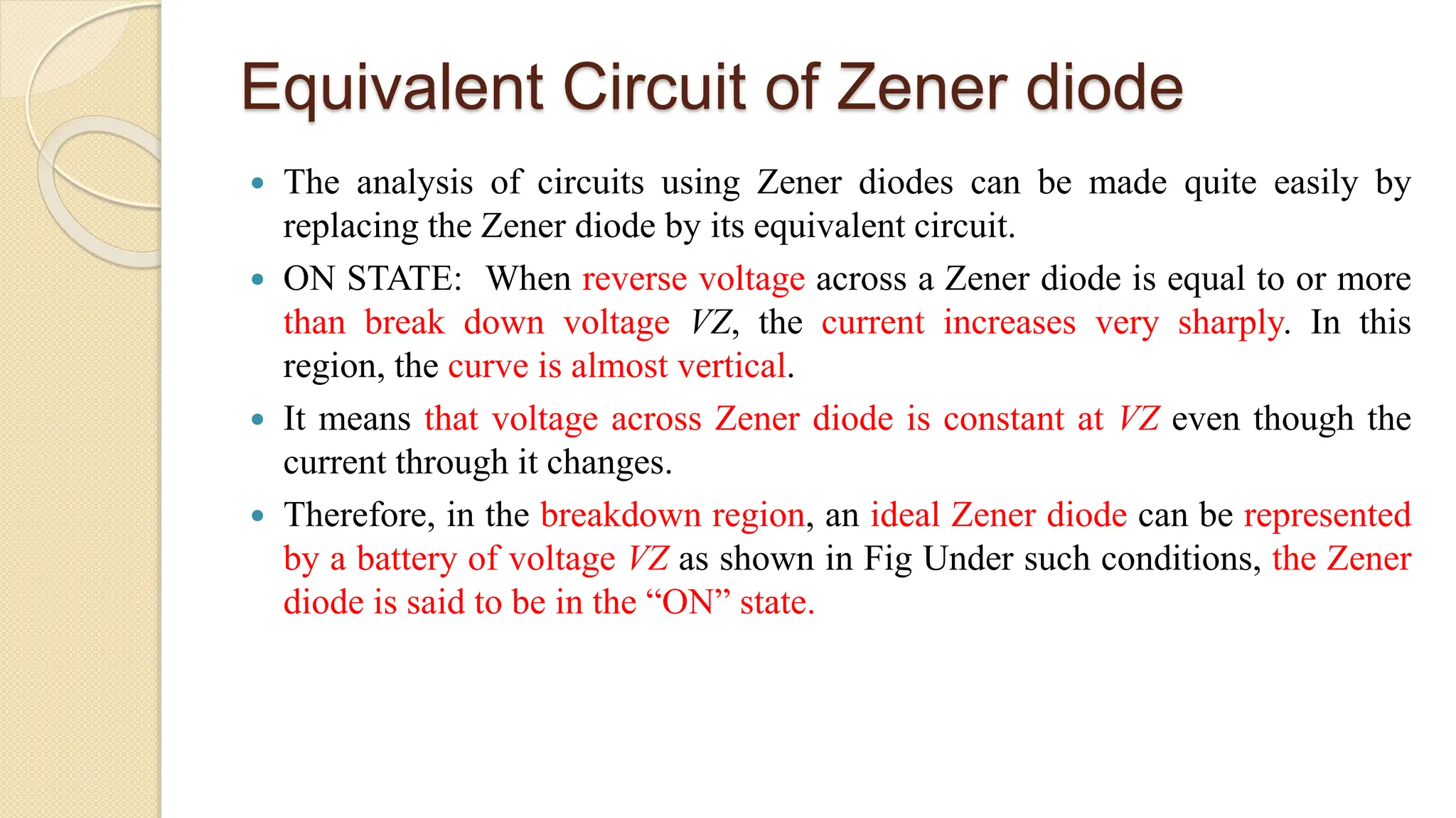
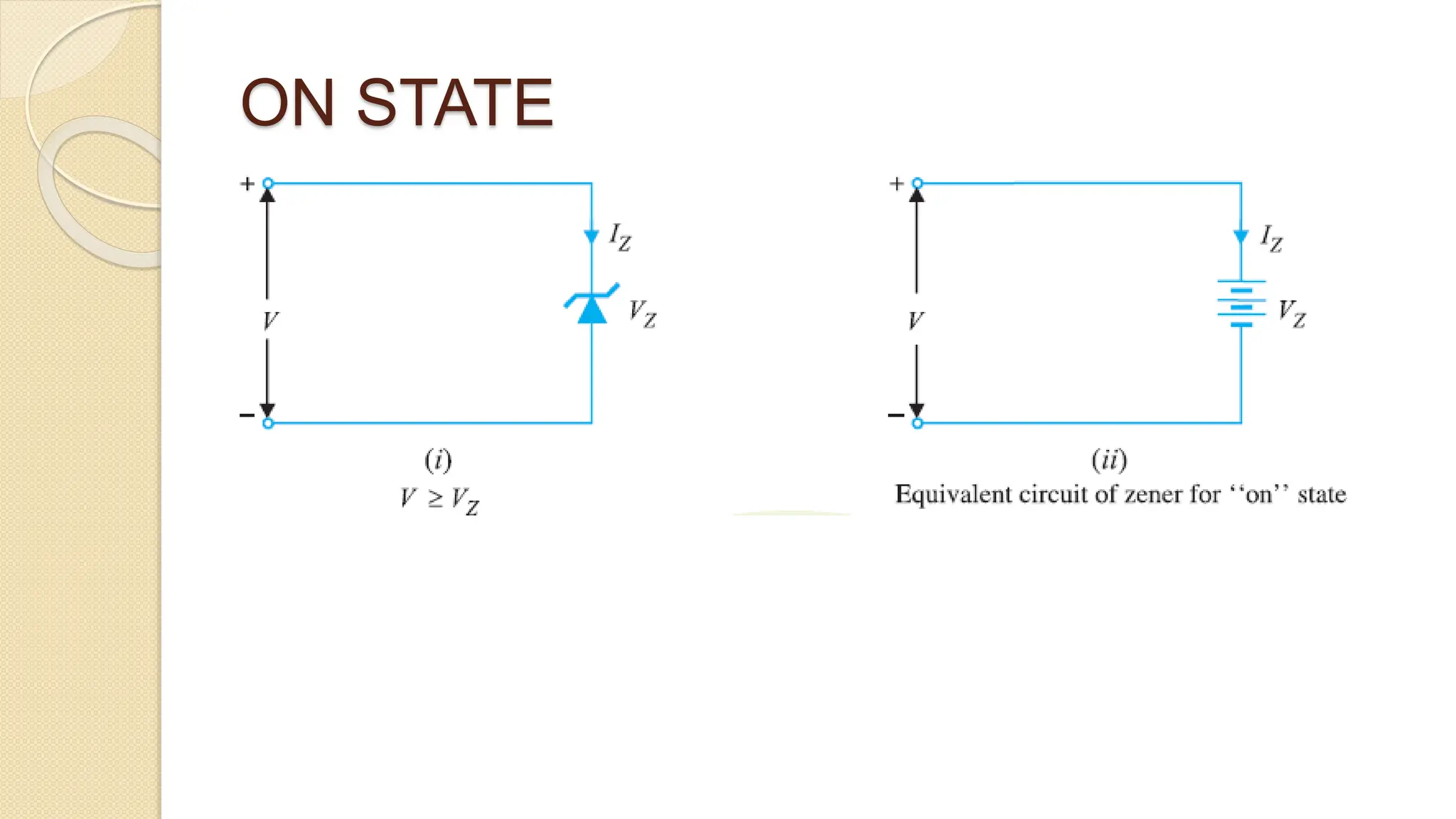
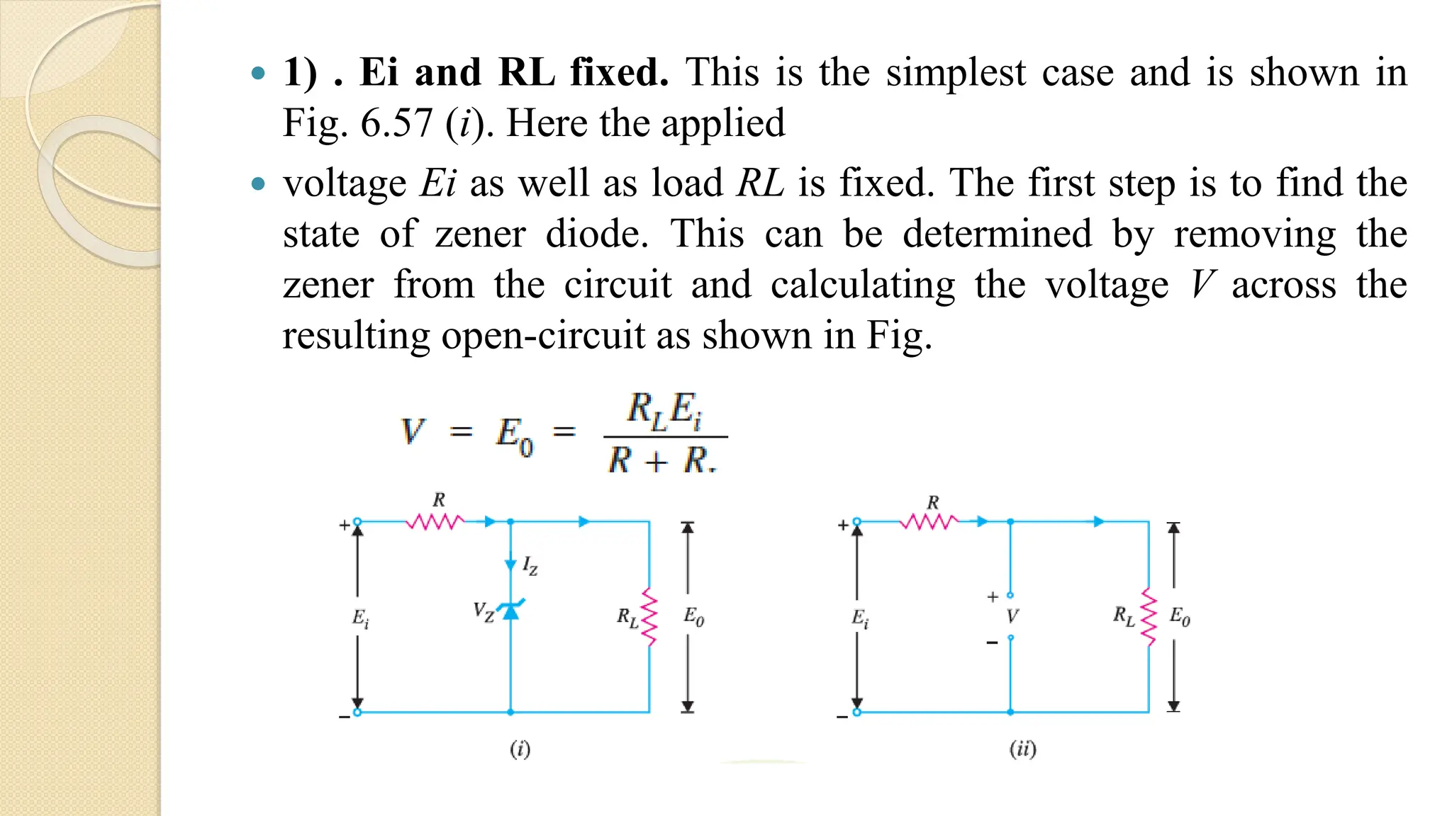
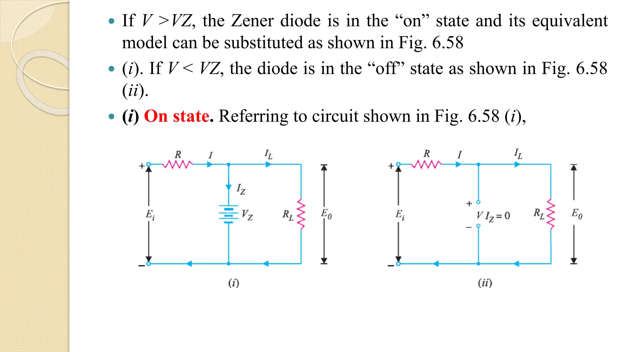
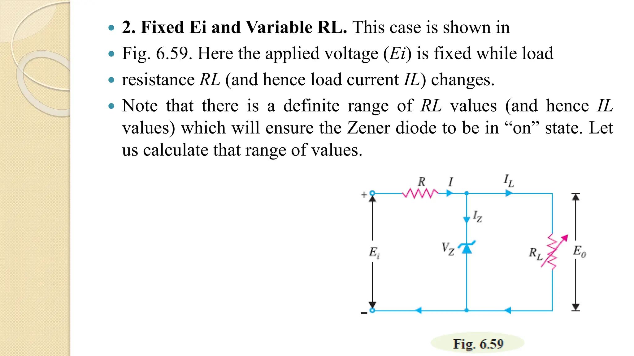
ZENER DIODE
 It has already been discussed that when the reverse bias on a
crystal diode is increased, a critical voltage, called breakdown
voltage is reached where the reverse current increases sharply to a
high value.
 The breakdown region is the knee of the reverse characteristic as
shown in Fig.
 The satisfactory explanation of this breakdown of the junction
was first given by the American scientist C. Zener.
 Therefore, the breakdown voltage is sometimes called Zener
voltage and the sudden increase in current is known as Zener
current.
Zener Diode Characteristics
 The breakdown or zener voltage depends upon the amount of
doping.
 If the diode is heavily doped, depletion layer will be thin and
consequently the breakdown of the junction will occur at a lower
reverse voltage.
 On the other hand, a lightly doped diode has a higher breakdown
voltage.
 When an ordinary crystal diode is properly doped so that it has a
sharp breakdown voltage, it is called a zener diode.
 “A properly doped crystal diode which has a sharp breakdown
voltage is known as a Zener diode.”
 It may be seen that it is just like an ordinary diode except that the bar is
turned into z-shape.
 The following points may be noted about the Zener diode:
 A Zener diode is like an ordinary diode except that it is properly doped so as
to have a sharp breakdown voltage.
 A Zener diode is always reverse connected i.e. it is always reverse biased.
 A Zener diode has sharp breakdown voltage, called Zener voltage VZ.
 When forward biased, its characteristics are just those of ordinary diode.
 The Zener diode is not immediately burnt just because it has entered the
breakdown region.
 As long as the external circuit connected to the diode limits the diode current
to less than burn out value, the diode will not burn out.
Equivalent Circuit of Zener diode
 The analysis of circuits using Zener diodes can be made quite easily by
replacing the Zener diode by its equivalent circuit.
 ON STATE: When reverse voltage across a Zener diode is equal to or more
than break down voltage VZ, the current increases very sharply. In this
region, the curve is almost vertical.
 It means that voltage across Zener diode is constant at VZ even though the
current through it changes.
 Therefore, in the breakdown region, an ideal Zener diode can be represented
by a battery of voltage VZ as shown in Fig Under such conditions, the Zener
diode is said to be in the “ON” state.
ON STATE
OFF STATE
 When the reverse voltage across the Zener diode is less than VZ
but greater than 0 V, the Zener diode is in the “OFF” state. Under
such conditions, the Zener diode can be represented by an open-
circuit as shown in Fig.
Zener Diode as Voltage Stabilizer
 A Zener diode can be used as a voltage regulator to provide a constant
voltage from a source whose voltage may vary over sufficient range.
 The circuit arrangement shown in fig
 The Zener diode of Zener voltage VZ is reverse connected across the load RL
across which constant output is desired.
 The series resistance R absorbs the output voltage fluctuations so as to
maintain constant voltage across the load.
 It may be noted that the Zener will maintain a constant voltage VZ (= E0)
across the load so long as the input voltage does not fall below VZ.
 When the circuit is properly designed, the load voltage E0 remains
essentially constant (equal to VZ) even though the input voltage Ei and load
resistance RL may vary over a wide range.
Zener Diode as Voltage
Stabilizer
 I) Suppose the input voltage increases. Since the Zener is in the
breakdown region, the Zener diode is equivalent to a battery VZ as
shown in Fig. 6.56 (ii).
 It is clear that output voltage remains constant at VZ (= E0). The excess
voltage is dropped across the series resistance R.
 This will cause an increase in the value of total current I. The Zener
will conduct the increase of current in I while the load current remains
constant. Hence, output voltage E0 remains constant irrespective of the
changes in the input voltage Ei.
 II) Now suppose that input voltage is constant but the load
resistance RL decreases. This will cause an increase in load
current. The extra current cannot come from the source because
drop in R (and hence source current I) will not change as the
Zener is within its regulating range.
 The additional load current will come from a decrease in Zener
current IZ. Consequently, the output voltage stays at constant
value.
Solving Zener Diode Circuits
 The analysis of Zener diode circuits is quite similar to that applied
to the analysis of semiconductor diodes.
 The first step is to determine the state of Zener diode i.e., whether
the Zener is in the “on” state or “off” state.
 Next, the Zener is replaced by its appropriate model. Finally, the
unknown quantities are determined from the resulting circuit.
 1) . Ei and RL fixed. This is the simplest case and is shown in
Fig. 6.57 (i). Here the applied
 voltage Ei as well as load RL is fixed. The first step is to find the
state of zener diode. This can be determined by removing the
zener from the circuit and calculating the voltage V across the
resulting open-circuit as shown in Fig.
 If V >VZ, the Zener diode is in the “on” state and its equivalent
model can be substituted as shown in Fig. 6.58
 (i). If V < VZ, the diode is in the “off” state as shown in Fig. 6.58
(ii).
 (i) On state. Referring to circuit shown in Fig. 6.58 (i),
 2. Fixed Ei and Variable RL. This case is shown in
 Fig. 6.59. Here the applied voltage (Ei) is fixed while load
 resistance RL (and hence load current IL) changes.
 Note that there is a definite range of RL values (and hence IL
values) which will ensure the Zener diode to be in “on” state. Let
us calculate that range of values.
 (i) RLmin and ILmax. Once the zener is in the “on”
 state, load voltage E0 (= VZ) is constant. As a result, when load
resistance is minimum (i.e., RLmin), load current
 will be maximum (IL = E0/RL).
 In order to find the minimum load resistance that will turn the
zener on, we simply calculate the value of R
 L that will result in E0 = VZ
 This is the minimum value of load resistance that will ensure that
zener is in the “on” state. Any value of load resistance less than
this value will result in a voltage E0 across the load less than VZ
and the zener will be in the “off” state.
 If the load resistance exceeds this limiting value, the current through Zener will exceed IZM
and the device may burn out.
 3. Fixed RL and Variable Ei. This case is shown in Fig. 6.60. Here the load
resistance RL is fixed while the applied voltage (Ei) changes. Note that there
is a definite range of Ei values that will ensure that zener diode is in the “on”
state. Let us calculate that range of values.
 (i) Ei (min). To determine the minimum applied voltage that will turn
the zener on, simply calculate the value of Ei that will result in load
voltage E0 = VZ
Crystal Diode Versus Vacuum Diode
 Advantages :
 (i) They are smaller, more rugged and have a longer life.
 (ii) They are simpler and inherently cheaper.
 (iii) They require no filament power. As a result, the produce less heat than
the equivalent vacuum diodes.
 Disadvantages :
 (i) They are extremely heat sensitive. Even a slight rise in temperature increases the
current appreciably.
 Should the temperature exceed the rated value of the diode, the increased flow of
current may produce enough heat to ruin the pn junction.
 On the other hand, vacuum diodes function normally over a wide range of
temperature changes.
 It may be noted that silicon is better than germanium as a semiconductor material.
Whereas a germanium diode should not be operated at temperatures higher than
80ºC, silicon diodes may operate safely at temperatures upto about 200ºC.
 (ii) They can handle small currents and low inverse voltages as compared to
vacuum diodes.
 (iii) They cannot stand an overload even for a short period. Any slight overload,
even a transient pulse, may permanently damage the crystal diode. On the other
hand, vacuum diodes can stand an overload for a short period and when the
overload is removed, the tube will generally recover.

ZENER DIODE AND ITS CHARACTERSITICS F

  • 1.
    ZENER DIODE  Ithas already been discussed that when the reverse bias on a crystal diode is increased, a critical voltage, called breakdown voltage is reached where the reverse current increases sharply to a high value.  The breakdown region is the knee of the reverse characteristic as shown in Fig.  The satisfactory explanation of this breakdown of the junction was first given by the American scientist C. Zener.  Therefore, the breakdown voltage is sometimes called Zener voltage and the sudden increase in current is known as Zener current.
  • 2.
  • 3.
     The breakdownor zener voltage depends upon the amount of doping.  If the diode is heavily doped, depletion layer will be thin and consequently the breakdown of the junction will occur at a lower reverse voltage.  On the other hand, a lightly doped diode has a higher breakdown voltage.  When an ordinary crystal diode is properly doped so that it has a sharp breakdown voltage, it is called a zener diode.  “A properly doped crystal diode which has a sharp breakdown voltage is known as a Zener diode.”
  • 4.
     It maybe seen that it is just like an ordinary diode except that the bar is turned into z-shape.  The following points may be noted about the Zener diode:  A Zener diode is like an ordinary diode except that it is properly doped so as to have a sharp breakdown voltage.  A Zener diode is always reverse connected i.e. it is always reverse biased.  A Zener diode has sharp breakdown voltage, called Zener voltage VZ.  When forward biased, its characteristics are just those of ordinary diode.  The Zener diode is not immediately burnt just because it has entered the breakdown region.  As long as the external circuit connected to the diode limits the diode current to less than burn out value, the diode will not burn out.
  • 5.
    Equivalent Circuit ofZener diode  The analysis of circuits using Zener diodes can be made quite easily by replacing the Zener diode by its equivalent circuit.  ON STATE: When reverse voltage across a Zener diode is equal to or more than break down voltage VZ, the current increases very sharply. In this region, the curve is almost vertical.  It means that voltage across Zener diode is constant at VZ even though the current through it changes.  Therefore, in the breakdown region, an ideal Zener diode can be represented by a battery of voltage VZ as shown in Fig Under such conditions, the Zener diode is said to be in the “ON” state.
  • 6.
  • 7.
    OFF STATE  Whenthe reverse voltage across the Zener diode is less than VZ but greater than 0 V, the Zener diode is in the “OFF” state. Under such conditions, the Zener diode can be represented by an open- circuit as shown in Fig.
  • 8.
    Zener Diode asVoltage Stabilizer  A Zener diode can be used as a voltage regulator to provide a constant voltage from a source whose voltage may vary over sufficient range.  The circuit arrangement shown in fig  The Zener diode of Zener voltage VZ is reverse connected across the load RL across which constant output is desired.  The series resistance R absorbs the output voltage fluctuations so as to maintain constant voltage across the load.  It may be noted that the Zener will maintain a constant voltage VZ (= E0) across the load so long as the input voltage does not fall below VZ.  When the circuit is properly designed, the load voltage E0 remains essentially constant (equal to VZ) even though the input voltage Ei and load resistance RL may vary over a wide range.
  • 9.
    Zener Diode asVoltage Stabilizer
  • 10.
     I) Supposethe input voltage increases. Since the Zener is in the breakdown region, the Zener diode is equivalent to a battery VZ as shown in Fig. 6.56 (ii).  It is clear that output voltage remains constant at VZ (= E0). The excess voltage is dropped across the series resistance R.  This will cause an increase in the value of total current I. The Zener will conduct the increase of current in I while the load current remains constant. Hence, output voltage E0 remains constant irrespective of the changes in the input voltage Ei.
  • 11.
     II) Nowsuppose that input voltage is constant but the load resistance RL decreases. This will cause an increase in load current. The extra current cannot come from the source because drop in R (and hence source current I) will not change as the Zener is within its regulating range.  The additional load current will come from a decrease in Zener current IZ. Consequently, the output voltage stays at constant value.
  • 12.
    Solving Zener DiodeCircuits  The analysis of Zener diode circuits is quite similar to that applied to the analysis of semiconductor diodes.  The first step is to determine the state of Zener diode i.e., whether the Zener is in the “on” state or “off” state.  Next, the Zener is replaced by its appropriate model. Finally, the unknown quantities are determined from the resulting circuit.
  • 13.
     1) .Ei and RL fixed. This is the simplest case and is shown in Fig. 6.57 (i). Here the applied  voltage Ei as well as load RL is fixed. The first step is to find the state of zener diode. This can be determined by removing the zener from the circuit and calculating the voltage V across the resulting open-circuit as shown in Fig.
  • 14.
     If V>VZ, the Zener diode is in the “on” state and its equivalent model can be substituted as shown in Fig. 6.58  (i). If V < VZ, the diode is in the “off” state as shown in Fig. 6.58 (ii).  (i) On state. Referring to circuit shown in Fig. 6.58 (i),
  • 16.
     2. FixedEi and Variable RL. This case is shown in  Fig. 6.59. Here the applied voltage (Ei) is fixed while load  resistance RL (and hence load current IL) changes.  Note that there is a definite range of RL values (and hence IL values) which will ensure the Zener diode to be in “on” state. Let us calculate that range of values.
  • 17.
     (i) RLminand ILmax. Once the zener is in the “on”  state, load voltage E0 (= VZ) is constant. As a result, when load resistance is minimum (i.e., RLmin), load current  will be maximum (IL = E0/RL).  In order to find the minimum load resistance that will turn the zener on, we simply calculate the value of R  L that will result in E0 = VZ
  • 18.
     This isthe minimum value of load resistance that will ensure that zener is in the “on” state. Any value of load resistance less than this value will result in a voltage E0 across the load less than VZ and the zener will be in the “off” state.  If the load resistance exceeds this limiting value, the current through Zener will exceed IZM and the device may burn out.
  • 19.
     3. FixedRL and Variable Ei. This case is shown in Fig. 6.60. Here the load resistance RL is fixed while the applied voltage (Ei) changes. Note that there is a definite range of Ei values that will ensure that zener diode is in the “on” state. Let us calculate that range of values.  (i) Ei (min). To determine the minimum applied voltage that will turn the zener on, simply calculate the value of Ei that will result in load voltage E0 = VZ
  • 28.
    Crystal Diode VersusVacuum Diode  Advantages :  (i) They are smaller, more rugged and have a longer life.  (ii) They are simpler and inherently cheaper.  (iii) They require no filament power. As a result, the produce less heat than the equivalent vacuum diodes.
  • 29.
     Disadvantages : (i) They are extremely heat sensitive. Even a slight rise in temperature increases the current appreciably.  Should the temperature exceed the rated value of the diode, the increased flow of current may produce enough heat to ruin the pn junction.  On the other hand, vacuum diodes function normally over a wide range of temperature changes.  It may be noted that silicon is better than germanium as a semiconductor material. Whereas a germanium diode should not be operated at temperatures higher than 80ºC, silicon diodes may operate safely at temperatures upto about 200ºC.  (ii) They can handle small currents and low inverse voltages as compared to vacuum diodes.  (iii) They cannot stand an overload even for a short period. Any slight overload, even a transient pulse, may permanently damage the crystal diode. On the other hand, vacuum diodes can stand an overload for a short period and when the overload is removed, the tube will generally recover.