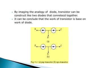
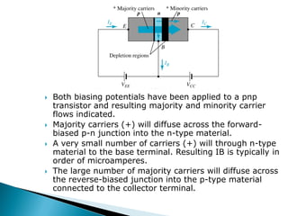
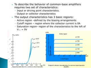
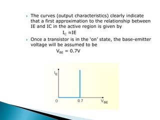
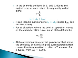
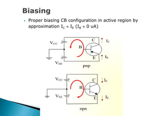
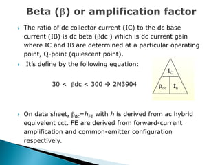
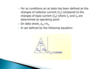
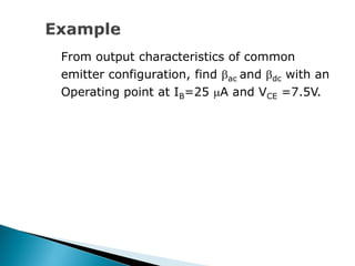
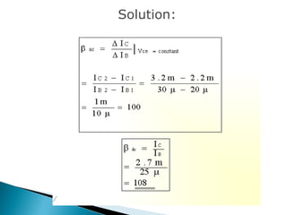
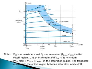
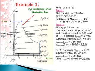
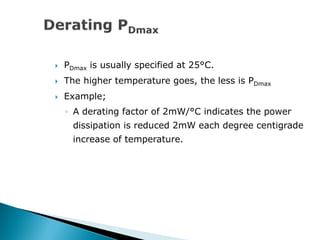
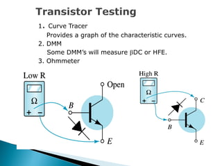
SlideShare a Scribd company logo
CHAPTER 3
 The basic of electronic system nowadays is
semiconductor device.
 The famous and commonly use of this device
is BJTs
(Bipolar Junction Transistors).
 It can be use as amplifier and logic switches.
 BJT consists of three terminal:
 collector : C
 base : B
emitter : E
 Two types of BJT : pnp and npn
 3 layer semiconductor device consisting:
◦ 2 n- and 1 p-type layers of material  npn transistor
◦ 2 p- and 1 n-type layers of material pnp transistor
 The term bipolar reflects the fact that holes and
electrons participate in the injection process into the
oppositely polarized material
 A single pn junction has two different types of bias:
◦ forward bias
◦ reverse bias
 Thus, a two-pn-junction device has four types of bias.
• Base is located at the middle
and more thin from the level
of collector and emitter
• The emitter and collector
terminals are made of the
same type of semiconductor
material, while the base of the
other type of material
-The arrow is always drawn
on the emitter
-The arrow always point
toward the n-type
-The arrow indicates the
direction of the emitter
current:
pnp:E B
npn: B E
IC=the collector current
IB= the base current
IE= the emitter current
 By imaging the analogy of diode, transistor can be
construct like two diodes that connetecd together.
 It can be conclude that the work of transistor is base on
work of diode.
 The basic operation will be described using the pnp
transistor. The operation of the pnp transistor is
exactly the same if the roles played by the electron
and hole are interchanged.
 One p-n junction of a transistor is reverse-biased,
whereas the other is forward-biased.
Forward-biased junction
of a pnp transistor
Reverse-biased junction
of a pnp transistor
 Both biasing potentials have been applied to a pnp
transistor and resulting majority and minority carrier
flows indicated.
 Majority carriers (+) will diffuse across the forward-
biased p-n junction into the n-type material.
 A very small number of carriers (+) will through n-type
material to the base terminal. Resulting IB is typically in
order of microamperes.
 The large number of majority carriers will diffuse across
the reverse-biased junction into the p-type material
connected to the collector terminal.
 Majority carriers can cross the reverse-biased
junction because the injected majority carriers will
appear as minority carriers in the n-type material.
 Applying KCL to the transistor :
IE = IC + IB
 The comprises of two components – the majority
and minority carriers
IC = ICmajority + ICOminority
 ICO – IC current with emitter terminal open and is
called leakage current.
 Common-base terminology is derived from the fact that
the :
- base is common to both input and output of the
configuration.
- base is usually the terminal closest to or at
ground potential.
 All current directions will refer to conventional (hole)
flow and the arrows in all electronic symbols have a
direction defined by this convention.
 Note that the applied biasing (voltage sources) are such
as to establish current in the direction indicated for
each branch.
 To describe the behavior of common-base amplifiers
requires two set of characteristics:
- Input or driving point characteristics.
- Output or collector characteristics
 The output characteristics has 3 basic regions:
- Active region –defined by the biasing arrangements
- Cutoff region – region where the collector current is 0A
- Saturation region- region of the characteristics to the left of
VCB = 0V
 The curves (output characteristics) clearly indicate
that a first approximation to the relationship between
IE and IC in the active region is given by
IC ≈IE
 Once a transistor is in the ‘on’ state, the base-emitter
voltage will be assumed to be
VBE = 0.7V
 In the dc mode the level of IC and IE due to the
majority carriers are related by a quantity called
alpha
=
IC = IE + ICBO
 It can then be summarize to IC = IE (ignore ICBO due
to small value)
 For ac situations where the point of operation moves
on the characteristics curve, an ac alpha defined by
 Alpha a common base current gain factor that shows
the efficiency by calculating the current percent from
current flow from emitter to collector.The value of 
is typical from 0.9 ~ 0.998.
E
C
I
I
E
C
I
I




 Proper biasing CB configuration in active region by
approximation IC  IE (IB  0 uA)
 It is called common-emitter configuration since :
- emitter is common or reference to both input and
output terminals.
- emitter is usually the terminal closest to or at
ground
potential.
 Almost amplifier design is using connection of CE due
to the high gain for current and voltage.
 Two set of characteristics are necessary to describe
the behavior for CE ;input (base terminal) and output
(collector terminal) parameters.
Proper Biasing common-emitter configuration in active region
Input characteristics for a
common-emitter NPN transistor
 IB is microamperes compared
to miliamperes of IC.
 IB will flow when VBE > 0.7V
for silicon and 0.3V for
germanium
 Before this value IB is very
small and no IB.
 Base-emitter junction is
forward bias
 Increasing VCE will reduce IB
for different values.
Output characteristics for a
common-emitter npn
transistor
 For small VCE (VCE < VCESAT, IC increase linearly with
increasing of VCE
 VCE > VCESAT IC not totally depends on VCE  constant IC
 IB(uA) is very small compare to IC (mA). Small increase in
IB cause big increase in IC
 IB=0 A  ICEO occur.
 Noticing the value when IC=0A. There is still some value of
current flows.
 The ratio of dc collector current (IC) to the dc base
current (IB) is dc beta (dc ) which is dc current gain
where IC and IB are determined at a particular operating
point, Q-point (quiescent point).
 It’s define by the following equation:
30 < dc < 300  2N3904
 On data sheet, dc=hFE with h is derived from ac hybrid
equivalent cct. FE are derived from forward-current
amplification and common-emitter configuration
respectively.
 For ac conditions an ac beta has been defined as the
changes of collector current (IC) compared to the
changes of base current (IB) where IC and IB are
determined at operating point.
 On data sheet, ac=hfe
 It can defined by the following equation:
From output characteristics of common
emitter configuration, find ac and dc with an
Operating point at IB=25 A and VCE =7.5V.
Solution:
 Also called emitter-follower (EF).
 It is called common-emitter configuration since both the
signal source and the load share the collector terminal
as a common connection point.
 The output voltage is obtained at emitter terminal.
 The input characteristic of common-collector
configuration is similar with common-emitter.
configuration.
 Common-collector circuit configuration is provided with
the load resistor connected from emitter to ground.
 It is used primarily for impedance-matching purpose
since it has high input impedance and low output
impedance.
Notation and symbols used with the common-collector configuration:
(a) pnp transistor ; (b) npn transistor.
 For the common-collector configuration, the output
characteristics are a plot of IE vs VCE for a range of values of
IB.
 Many BJT transistor used as an amplifier. Thus it is
important to notice the limits of operations.
 At least 3 maximum values is mentioned in data sheet.
 There are:
a) Maximum power dissipation at collector: PCmax
or PD
b) Maximum collector-emitter voltage: VCEmax
sometimes named as VBR(CEO) or VCEO.
c) Maximum collector current: ICmax
 There are few rules that need to be followed for BJT
transistor used as an amplifier. The rules are:
i) transistor need to be operate in active region!
ii) IC < ICmax
ii) PC < PCmax
Note: VCE is at maximum and IC is at minimum (ICmax=ICEO) in the
cutoff region. IC is at maximum and VCE is at minimum
(VCE max = VCEsat = VCEO) in the saturation region. The transistor
operates in the active region between saturation and cutoff.
Refer to the fig.
Step1:
The maximum collector
power dissipation,
PD=ICmax x VCEmax (1)
= 18m x 20 = 360 mW
Step 2:
At any point on the
characteristics the product of
and must be equal to 360 mW.
Ex. 1. If choose ICmax= 5 mA,
subtitute into the (1), we get
VCEmaxICmax= 360 mW
VCEmax(5 m)=360/5=7.2 V
Ex.2. If choose VCEmax=18 V,
subtitute into (1), we get
VCEmaxICmax= 360 mW
(10) ICmax=360m/18=20 mA
 PDmax is usually specified at 25°C.
 The higher temperature goes, the less is PDmax
 Example;
◦ A derating factor of 2mW/°C indicates the power
dissipation is reduced 2mW each degree centigrade
increase of temperature.
Transistor 2N3904 used in the circuit with
VCE=20 V. This circuit used at temperature
1250C. Calculate the new maximum IC.
Transistor 2N3904 have maximum power
dissipation is 625 mW. Derating factor is
5mW/0C.
 Step 1:
Temperature increase : 1250C – 250C = 1000C
 Step 2:
Derate transistor : 5 mW/0C x 1000C = 500 mW
 Step 3:
Maximum power dissipation at 1250C = 625 mW–500
mW=125 mW.
 Step 4:
Thus ICmax = PCmax / VCE=125m/20 = 6.25 mA.
 Step 5:
Draw the new line of power dissipation at 1250C .
The parameters of transistor 2N3055 as follows:
- Maximum power dissipation @ 250C=115 W
- Derate factor=0.66 mW/0C.
This transistor used at temperature 780C.
Find the new maximum value of power dissipation.
Find the set of new maximum of IC if VCE=10V,
20V and 40 V.
 Step 1:
Temperature increase : 780C – 250C = 530C
 Step 2:
Derate transistor : 0.66mW/0C x 530C = 35 mW
 Step 3:
Maximum power dissipation at 780C = 115W– 35W=80
mW.
 Step 4:
ICmax = PCmax / VCE=80m/10 = 8 mA (point C)
ICmax = PCmax / VCE=80m/20 = 4 mA. (point B)
ICmax = PCmax / VCE=80m/40 = 2 mA (point A)
Step 5:
Draw the new line of power dissipation at 780C .
1. Curve Tracer
Provides a graph of the characteristic curves.
2. DMM
Some DMM’s will measure DC or HFE.
3. Ohmmeter

More Related Content

Similar to BJT - Bipolar Junction Transistor / Electron Devices

Transistor Configuration
Transistor Configuration Transistor Configuration
Transistor Configuration Smit Shah
 
Phy 4240 lec (9) and (10)
Phy 4240 lec (9) and (10)Phy 4240 lec (9) and (10)
Phy 4240 lec (9) and (10)Dr. Abeer Kamal
 
BJT Basic and Biasing-Abridged(1).pptx
BJT Basic and Biasing-Abridged(1).pptxBJT Basic and Biasing-Abridged(1).pptx
BJT Basic and Biasing-Abridged(1).pptxNimishDuggal1
 
Transistor Fundamentals
Transistor FundamentalsTransistor Fundamentals
Transistor FundamentalsJay Baria
 
Bjt(common base ,emitter,collector) from university of central punjab
Bjt(common base ,emitter,collector) from university of central punjabBjt(common base ,emitter,collector) from university of central punjab
Bjt(common base ,emitter,collector) from university of central punjabKhawaja Shazy
 
(Latest) topic 4 bipolar_junction_transistors
(Latest) topic 4 bipolar_junction_transistors(Latest) topic 4 bipolar_junction_transistors
(Latest) topic 4 bipolar_junction_transistorsGabriel O'Brien
 
Bipolar Transistor
Bipolar TransistorBipolar Transistor
Bipolar TransistorUMAR ALI
 
Chapter 6: Bipolar Junction Transistors (BJTs)
Chapter 6: Bipolar Junction Transistors (BJTs)Chapter 6: Bipolar Junction Transistors (BJTs)
Chapter 6: Bipolar Junction Transistors (BJTs)JeremyLauKarHei
 
Basic electronics - Bi Junction Terminals 01.pptx
Basic electronics - Bi Junction Terminals 01.pptxBasic electronics - Bi Junction Terminals 01.pptx
Basic electronics - Bi Junction Terminals 01.pptxhappycocoman
 
BJT by Emroz Sardar.pptx
BJT by Emroz Sardar.pptxBJT by Emroz Sardar.pptx
BJT by Emroz Sardar.pptxEmroz Sardar
 
Transistor, MOSFET and Operational Amplr
Transistor, MOSFET and Operational AmplrTransistor, MOSFET and Operational Amplr
Transistor, MOSFET and Operational AmplrHarshalVaidya11
 
Bipolar junction transistor characterstics biassing and amplification, lab 9
Bipolar junction transistor characterstics biassing and amplification, lab 9Bipolar junction transistor characterstics biassing and amplification, lab 9
Bipolar junction transistor characterstics biassing and amplification, lab 9kehali Haileselassie
 
Electronics 1 : Chapter # 06 : Bipolar Junction Transistor
Electronics 1 : Chapter # 06 : Bipolar Junction TransistorElectronics 1 : Chapter # 06 : Bipolar Junction Transistor
Electronics 1 : Chapter # 06 : Bipolar Junction TransistorSk_Group
 

Similar to BJT - Bipolar Junction Transistor / Electron Devices (20)

Transistor Configuration
Transistor Configuration Transistor Configuration
Transistor Configuration
 
Phy 4240 lec (9) and (10)
Phy 4240 lec (9) and (10)Phy 4240 lec (9) and (10)
Phy 4240 lec (9) and (10)
 
BJT Basic and Biasing-Abridged(1).pptx
BJT Basic and Biasing-Abridged(1).pptxBJT Basic and Biasing-Abridged(1).pptx
BJT Basic and Biasing-Abridged(1).pptx
 
Unit 3
Unit 3Unit 3
Unit 3
 
Transistor Fundamentals
Transistor FundamentalsTransistor Fundamentals
Transistor Fundamentals
 
Bjt(common base ,emitter,collector) from university of central punjab
Bjt(common base ,emitter,collector) from university of central punjabBjt(common base ,emitter,collector) from university of central punjab
Bjt(common base ,emitter,collector) from university of central punjab
 
Cbcs e1 unit 3
Cbcs e1 unit 3Cbcs e1 unit 3
Cbcs e1 unit 3
 
ADE UNIT-2.pptx
ADE UNIT-2.pptxADE UNIT-2.pptx
ADE UNIT-2.pptx
 
Lecture 8M.pptx
Lecture 8M.pptxLecture 8M.pptx
Lecture 8M.pptx
 
(Latest) topic 4 bipolar_junction_transistors
(Latest) topic 4 bipolar_junction_transistors(Latest) topic 4 bipolar_junction_transistors
(Latest) topic 4 bipolar_junction_transistors
 
Bipolar Transistor
Bipolar TransistorBipolar Transistor
Bipolar Transistor
 
Chapter 6: Bipolar Junction Transistors (BJTs)
Chapter 6: Bipolar Junction Transistors (BJTs)Chapter 6: Bipolar Junction Transistors (BJTs)
Chapter 6: Bipolar Junction Transistors (BJTs)
 
Lecture 8 bjt_1
Lecture 8 bjt_1Lecture 8 bjt_1
Lecture 8 bjt_1
 
Basic electronics - Bi Junction Terminals 01.pptx
Basic electronics - Bi Junction Terminals 01.pptxBasic electronics - Bi Junction Terminals 01.pptx
Basic electronics - Bi Junction Terminals 01.pptx
 
BJT by Emroz Sardar.pptx
BJT by Emroz Sardar.pptxBJT by Emroz Sardar.pptx
BJT by Emroz Sardar.pptx
 
Transistor, MOSFET and Operational Amplr
Transistor, MOSFET and Operational AmplrTransistor, MOSFET and Operational Amplr
Transistor, MOSFET and Operational Amplr
 
Bipolar junction transistor characterstics biassing and amplification, lab 9
Bipolar junction transistor characterstics biassing and amplification, lab 9Bipolar junction transistor characterstics biassing and amplification, lab 9
Bipolar junction transistor characterstics biassing and amplification, lab 9
 
Bipolar junction transistor characterstics biassing and amplification, lab 9
Bipolar junction transistor characterstics biassing and amplification, lab 9Bipolar junction transistor characterstics biassing and amplification, lab 9
Bipolar junction transistor characterstics biassing and amplification, lab 9
 
Electronics 1 : Chapter # 06 : Bipolar Junction Transistor
Electronics 1 : Chapter # 06 : Bipolar Junction TransistorElectronics 1 : Chapter # 06 : Bipolar Junction Transistor
Electronics 1 : Chapter # 06 : Bipolar Junction Transistor
 
Transistor configurations
Transistor configurationsTransistor configurations
Transistor configurations
 

More from Shiny Christobel

DSP Module -5 Multirate Signal Processing and its applications
DSP Module -5 Multirate Signal Processing and its applicationsDSP Module -5 Multirate Signal Processing and its applications
DSP Module -5 Multirate Signal Processing and its applicationsShiny Christobel
 
DSP Module-4 Finite Wordlength Effect and Zero Limit Cycle
DSP Module-4 Finite Wordlength Effect and Zero Limit CycleDSP Module-4 Finite Wordlength Effect and Zero Limit Cycle
DSP Module-4 Finite Wordlength Effect and Zero Limit CycleShiny Christobel
 
DSP - Realization of Finite Impulse Response Filter
DSP -  Realization of  Finite Impulse Response FilterDSP -  Realization of  Finite Impulse Response Filter
DSP - Realization of Finite Impulse Response FilterShiny Christobel
 
circular convolution and Linear convolution
circular convolution and Linear convolutioncircular convolution and Linear convolution
circular convolution and Linear convolutionShiny Christobel
 
DFT - Discrete Fourier Transform and its Properties
DFT - Discrete Fourier Transform and its PropertiesDFT - Discrete Fourier Transform and its Properties
DFT - Discrete Fourier Transform and its PropertiesShiny Christobel
 
Transducers and Data Aquisition Systems.pdf
Transducers and Data Aquisition Systems.pdfTransducers and Data Aquisition Systems.pdf
Transducers and Data Aquisition Systems.pdfShiny Christobel
 

More from Shiny Christobel (8)

DSP Module -5 Multirate Signal Processing and its applications
DSP Module -5 Multirate Signal Processing and its applicationsDSP Module -5 Multirate Signal Processing and its applications
DSP Module -5 Multirate Signal Processing and its applications
 
DSP Module-4 Finite Wordlength Effect and Zero Limit Cycle
DSP Module-4 Finite Wordlength Effect and Zero Limit CycleDSP Module-4 Finite Wordlength Effect and Zero Limit Cycle
DSP Module-4 Finite Wordlength Effect and Zero Limit Cycle
 
DSP - Realization of Finite Impulse Response Filter
DSP -  Realization of  Finite Impulse Response FilterDSP -  Realization of  Finite Impulse Response Filter
DSP - Realization of Finite Impulse Response Filter
 
circular convolution and Linear convolution
circular convolution and Linear convolutioncircular convolution and Linear convolution
circular convolution and Linear convolution
 
DFT - Discrete Fourier Transform and its Properties
DFT - Discrete Fourier Transform and its PropertiesDFT - Discrete Fourier Transform and its Properties
DFT - Discrete Fourier Transform and its Properties
 
Transducers and Data Aquisition Systems.pdf
Transducers and Data Aquisition Systems.pdfTransducers and Data Aquisition Systems.pdf
Transducers and Data Aquisition Systems.pdf
 
Semiconductors
SemiconductorsSemiconductors
Semiconductors
 
DSP PPT
DSP PPTDSP PPT
DSP PPT
 

Recently uploaded

KIT-601 Lecture Notes-UNIT-4.pdf Frequent Itemsets and Clustering
KIT-601 Lecture Notes-UNIT-4.pdf Frequent Itemsets and ClusteringKIT-601 Lecture Notes-UNIT-4.pdf Frequent Itemsets and Clustering
KIT-601 Lecture Notes-UNIT-4.pdf Frequent Itemsets and ClusteringDr. Radhey Shyam
 
Pharmacy management system project report..pdf
Pharmacy management system project report..pdfPharmacy management system project report..pdf
Pharmacy management system project report..pdfKamal Acharya
 
2024 DevOps Pro Europe - Growing at the edge
2024 DevOps Pro Europe - Growing at the edge2024 DevOps Pro Europe - Growing at the edge
2024 DevOps Pro Europe - Growing at the edgePaco Orozco
 
School management system project report.pdf
School management system project report.pdfSchool management system project report.pdf
School management system project report.pdfKamal Acharya
 
İTÜ CAD and Reverse Engineering Workshop
İTÜ CAD and Reverse Engineering WorkshopİTÜ CAD and Reverse Engineering Workshop
İTÜ CAD and Reverse Engineering WorkshopEmre Günaydın
 
Activity Planning: Objectives, Project Schedule, Network Planning Model. Time...
Activity Planning: Objectives, Project Schedule, Network Planning Model. Time...Activity Planning: Objectives, Project Schedule, Network Planning Model. Time...
Activity Planning: Objectives, Project Schedule, Network Planning Model. Time...Lovely Professional University
 
Peek implant persentation - Copy (1).pdf
Peek implant persentation - Copy (1).pdfPeek implant persentation - Copy (1).pdf
Peek implant persentation - Copy (1).pdfAyahmorsy
 
Online blood donation management system project.pdf
Online blood donation management system project.pdfOnline blood donation management system project.pdf
Online blood donation management system project.pdfKamal Acharya
 
internship exam ppt.pptx on embedded system and IOT
internship exam ppt.pptx on embedded system and IOTinternship exam ppt.pptx on embedded system and IOT
internship exam ppt.pptx on embedded system and IOTNavyashreeS6
 
Online resume builder management system project report.pdf
Online resume builder management system project report.pdfOnline resume builder management system project report.pdf
Online resume builder management system project report.pdfKamal Acharya
 
KIT-601 Lecture Notes-UNIT-3.pdf Mining Data Stream
KIT-601 Lecture Notes-UNIT-3.pdf Mining Data StreamKIT-601 Lecture Notes-UNIT-3.pdf Mining Data Stream
KIT-601 Lecture Notes-UNIT-3.pdf Mining Data StreamDr. Radhey Shyam
 
Electrical shop management system project report.pdf
Electrical shop management system project report.pdfElectrical shop management system project report.pdf
Electrical shop management system project report.pdfKamal Acharya
 
An improvement in the safety of big data using blockchain technology
An improvement in the safety of big data using blockchain technologyAn improvement in the safety of big data using blockchain technology
An improvement in the safety of big data using blockchain technologyBOHRInternationalJou1
 
ONLINE CAR SERVICING SYSTEM PROJECT REPORT.pdf
ONLINE CAR SERVICING SYSTEM PROJECT REPORT.pdfONLINE CAR SERVICING SYSTEM PROJECT REPORT.pdf
ONLINE CAR SERVICING SYSTEM PROJECT REPORT.pdfKamal Acharya
 
"United Nations Park" Site Visit Report.
"United Nations Park" Site  Visit Report."United Nations Park" Site  Visit Report.
"United Nations Park" Site Visit Report.MdManikurRahman
 
NO1 Pandit Black Magic Removal in Uk kala jadu Specialist kala jadu for Love ...
NO1 Pandit Black Magic Removal in Uk kala jadu Specialist kala jadu for Love ...NO1 Pandit Black Magic Removal in Uk kala jadu Specialist kala jadu for Love ...
NO1 Pandit Black Magic Removal in Uk kala jadu Specialist kala jadu for Love ...Amil baba
 
BRAKING SYSTEM IN INDIAN RAILWAY AutoCAD DRAWING
BRAKING SYSTEM IN INDIAN RAILWAY AutoCAD DRAWINGBRAKING SYSTEM IN INDIAN RAILWAY AutoCAD DRAWING
BRAKING SYSTEM IN INDIAN RAILWAY AutoCAD DRAWINGKOUSTAV SARKAR
 
Introduction to Machine Learning Unit-4 Notes for II-II Mechanical Engineering
Introduction to Machine Learning Unit-4 Notes for II-II Mechanical EngineeringIntroduction to Machine Learning Unit-4 Notes for II-II Mechanical Engineering
Introduction to Machine Learning Unit-4 Notes for II-II Mechanical EngineeringC Sai Kiran
 
Software Engineering - Modelling Concepts + Class Modelling + Building the An...
Software Engineering - Modelling Concepts + Class Modelling + Building the An...Software Engineering - Modelling Concepts + Class Modelling + Building the An...
Software Engineering - Modelling Concepts + Class Modelling + Building the An...Prakhyath Rai
 
RM&IPR M5 notes.pdfResearch Methodolgy & Intellectual Property Rights Series 5
RM&IPR M5 notes.pdfResearch Methodolgy & Intellectual Property Rights Series 5RM&IPR M5 notes.pdfResearch Methodolgy & Intellectual Property Rights Series 5
RM&IPR M5 notes.pdfResearch Methodolgy & Intellectual Property Rights Series 5T.D. Shashikala
 

Recently uploaded (20)

KIT-601 Lecture Notes-UNIT-4.pdf Frequent Itemsets and Clustering
KIT-601 Lecture Notes-UNIT-4.pdf Frequent Itemsets and ClusteringKIT-601 Lecture Notes-UNIT-4.pdf Frequent Itemsets and Clustering
KIT-601 Lecture Notes-UNIT-4.pdf Frequent Itemsets and Clustering
 
Pharmacy management system project report..pdf
Pharmacy management system project report..pdfPharmacy management system project report..pdf
Pharmacy management system project report..pdf
 
2024 DevOps Pro Europe - Growing at the edge
2024 DevOps Pro Europe - Growing at the edge2024 DevOps Pro Europe - Growing at the edge
2024 DevOps Pro Europe - Growing at the edge
 
School management system project report.pdf
School management system project report.pdfSchool management system project report.pdf
School management system project report.pdf
 
İTÜ CAD and Reverse Engineering Workshop
İTÜ CAD and Reverse Engineering WorkshopİTÜ CAD and Reverse Engineering Workshop
İTÜ CAD and Reverse Engineering Workshop
 
Activity Planning: Objectives, Project Schedule, Network Planning Model. Time...
Activity Planning: Objectives, Project Schedule, Network Planning Model. Time...Activity Planning: Objectives, Project Schedule, Network Planning Model. Time...
Activity Planning: Objectives, Project Schedule, Network Planning Model. Time...
 
Peek implant persentation - Copy (1).pdf
Peek implant persentation - Copy (1).pdfPeek implant persentation - Copy (1).pdf
Peek implant persentation - Copy (1).pdf
 
Online blood donation management system project.pdf
Online blood donation management system project.pdfOnline blood donation management system project.pdf
Online blood donation management system project.pdf
 
internship exam ppt.pptx on embedded system and IOT
internship exam ppt.pptx on embedded system and IOTinternship exam ppt.pptx on embedded system and IOT
internship exam ppt.pptx on embedded system and IOT
 
Online resume builder management system project report.pdf
Online resume builder management system project report.pdfOnline resume builder management system project report.pdf
Online resume builder management system project report.pdf
 
KIT-601 Lecture Notes-UNIT-3.pdf Mining Data Stream
KIT-601 Lecture Notes-UNIT-3.pdf Mining Data StreamKIT-601 Lecture Notes-UNIT-3.pdf Mining Data Stream
KIT-601 Lecture Notes-UNIT-3.pdf Mining Data Stream
 
Electrical shop management system project report.pdf
Electrical shop management system project report.pdfElectrical shop management system project report.pdf
Electrical shop management system project report.pdf
 
An improvement in the safety of big data using blockchain technology
An improvement in the safety of big data using blockchain technologyAn improvement in the safety of big data using blockchain technology
An improvement in the safety of big data using blockchain technology
 
ONLINE CAR SERVICING SYSTEM PROJECT REPORT.pdf
ONLINE CAR SERVICING SYSTEM PROJECT REPORT.pdfONLINE CAR SERVICING SYSTEM PROJECT REPORT.pdf
ONLINE CAR SERVICING SYSTEM PROJECT REPORT.pdf
 
"United Nations Park" Site Visit Report.
"United Nations Park" Site  Visit Report."United Nations Park" Site  Visit Report.
"United Nations Park" Site Visit Report.
 
NO1 Pandit Black Magic Removal in Uk kala jadu Specialist kala jadu for Love ...
NO1 Pandit Black Magic Removal in Uk kala jadu Specialist kala jadu for Love ...NO1 Pandit Black Magic Removal in Uk kala jadu Specialist kala jadu for Love ...
NO1 Pandit Black Magic Removal in Uk kala jadu Specialist kala jadu for Love ...
 
BRAKING SYSTEM IN INDIAN RAILWAY AutoCAD DRAWING
BRAKING SYSTEM IN INDIAN RAILWAY AutoCAD DRAWINGBRAKING SYSTEM IN INDIAN RAILWAY AutoCAD DRAWING
BRAKING SYSTEM IN INDIAN RAILWAY AutoCAD DRAWING
 
Introduction to Machine Learning Unit-4 Notes for II-II Mechanical Engineering
Introduction to Machine Learning Unit-4 Notes for II-II Mechanical EngineeringIntroduction to Machine Learning Unit-4 Notes for II-II Mechanical Engineering
Introduction to Machine Learning Unit-4 Notes for II-II Mechanical Engineering
 
Software Engineering - Modelling Concepts + Class Modelling + Building the An...
Software Engineering - Modelling Concepts + Class Modelling + Building the An...Software Engineering - Modelling Concepts + Class Modelling + Building the An...
Software Engineering - Modelling Concepts + Class Modelling + Building the An...
 
RM&IPR M5 notes.pdfResearch Methodolgy & Intellectual Property Rights Series 5
RM&IPR M5 notes.pdfResearch Methodolgy & Intellectual Property Rights Series 5RM&IPR M5 notes.pdfResearch Methodolgy & Intellectual Property Rights Series 5
RM&IPR M5 notes.pdfResearch Methodolgy & Intellectual Property Rights Series 5
 

BJT - Bipolar Junction Transistor / Electron Devices

  • 2.  The basic of electronic system nowadays is semiconductor device.  The famous and commonly use of this device is BJTs (Bipolar Junction Transistors).  It can be use as amplifier and logic switches.  BJT consists of three terminal:  collector : C  base : B emitter : E  Two types of BJT : pnp and npn
  • 3.  3 layer semiconductor device consisting: ◦ 2 n- and 1 p-type layers of material  npn transistor ◦ 2 p- and 1 n-type layers of material pnp transistor  The term bipolar reflects the fact that holes and electrons participate in the injection process into the oppositely polarized material  A single pn junction has two different types of bias: ◦ forward bias ◦ reverse bias  Thus, a two-pn-junction device has four types of bias.
  • 4. • Base is located at the middle and more thin from the level of collector and emitter • The emitter and collector terminals are made of the same type of semiconductor material, while the base of the other type of material
  • 5. -The arrow is always drawn on the emitter -The arrow always point toward the n-type -The arrow indicates the direction of the emitter current: pnp:E B npn: B E IC=the collector current IB= the base current IE= the emitter current
  • 6.  By imaging the analogy of diode, transistor can be construct like two diodes that connetecd together.  It can be conclude that the work of transistor is base on work of diode.
  • 7.  The basic operation will be described using the pnp transistor. The operation of the pnp transistor is exactly the same if the roles played by the electron and hole are interchanged.  One p-n junction of a transistor is reverse-biased, whereas the other is forward-biased. Forward-biased junction of a pnp transistor Reverse-biased junction of a pnp transistor
  • 8.  Both biasing potentials have been applied to a pnp transistor and resulting majority and minority carrier flows indicated.  Majority carriers (+) will diffuse across the forward- biased p-n junction into the n-type material.  A very small number of carriers (+) will through n-type material to the base terminal. Resulting IB is typically in order of microamperes.  The large number of majority carriers will diffuse across the reverse-biased junction into the p-type material connected to the collector terminal.
  • 9.  Majority carriers can cross the reverse-biased junction because the injected majority carriers will appear as minority carriers in the n-type material.  Applying KCL to the transistor : IE = IC + IB  The comprises of two components – the majority and minority carriers IC = ICmajority + ICOminority  ICO – IC current with emitter terminal open and is called leakage current.
  • 10.  Common-base terminology is derived from the fact that the : - base is common to both input and output of the configuration. - base is usually the terminal closest to or at ground potential.  All current directions will refer to conventional (hole) flow and the arrows in all electronic symbols have a direction defined by this convention.  Note that the applied biasing (voltage sources) are such as to establish current in the direction indicated for each branch.
  • 11.
  • 12.  To describe the behavior of common-base amplifiers requires two set of characteristics: - Input or driving point characteristics. - Output or collector characteristics  The output characteristics has 3 basic regions: - Active region –defined by the biasing arrangements - Cutoff region – region where the collector current is 0A - Saturation region- region of the characteristics to the left of VCB = 0V
  • 13.
  • 14.  The curves (output characteristics) clearly indicate that a first approximation to the relationship between IE and IC in the active region is given by IC ≈IE  Once a transistor is in the ‘on’ state, the base-emitter voltage will be assumed to be VBE = 0.7V
  • 15.  In the dc mode the level of IC and IE due to the majority carriers are related by a quantity called alpha = IC = IE + ICBO  It can then be summarize to IC = IE (ignore ICBO due to small value)  For ac situations where the point of operation moves on the characteristics curve, an ac alpha defined by  Alpha a common base current gain factor that shows the efficiency by calculating the current percent from current flow from emitter to collector.The value of  is typical from 0.9 ~ 0.998. E C I I E C I I    
  • 16.  Proper biasing CB configuration in active region by approximation IC  IE (IB  0 uA)
  • 17.
  • 18.
  • 19.  It is called common-emitter configuration since : - emitter is common or reference to both input and output terminals. - emitter is usually the terminal closest to or at ground potential.  Almost amplifier design is using connection of CE due to the high gain for current and voltage.  Two set of characteristics are necessary to describe the behavior for CE ;input (base terminal) and output (collector terminal) parameters.
  • 20. Proper Biasing common-emitter configuration in active region
  • 21. Input characteristics for a common-emitter NPN transistor  IB is microamperes compared to miliamperes of IC.  IB will flow when VBE > 0.7V for silicon and 0.3V for germanium  Before this value IB is very small and no IB.  Base-emitter junction is forward bias  Increasing VCE will reduce IB for different values.
  • 22. Output characteristics for a common-emitter npn transistor  For small VCE (VCE < VCESAT, IC increase linearly with increasing of VCE  VCE > VCESAT IC not totally depends on VCE  constant IC  IB(uA) is very small compare to IC (mA). Small increase in IB cause big increase in IC  IB=0 A  ICEO occur.  Noticing the value when IC=0A. There is still some value of current flows.
  • 23.
  • 24.  The ratio of dc collector current (IC) to the dc base current (IB) is dc beta (dc ) which is dc current gain where IC and IB are determined at a particular operating point, Q-point (quiescent point).  It’s define by the following equation: 30 < dc < 300  2N3904  On data sheet, dc=hFE with h is derived from ac hybrid equivalent cct. FE are derived from forward-current amplification and common-emitter configuration respectively.
  • 25.  For ac conditions an ac beta has been defined as the changes of collector current (IC) compared to the changes of base current (IB) where IC and IB are determined at operating point.  On data sheet, ac=hfe  It can defined by the following equation:
  • 26. From output characteristics of common emitter configuration, find ac and dc with an Operating point at IB=25 A and VCE =7.5V.
  • 28.
  • 29.
  • 30.  Also called emitter-follower (EF).  It is called common-emitter configuration since both the signal source and the load share the collector terminal as a common connection point.  The output voltage is obtained at emitter terminal.  The input characteristic of common-collector configuration is similar with common-emitter. configuration.  Common-collector circuit configuration is provided with the load resistor connected from emitter to ground.  It is used primarily for impedance-matching purpose since it has high input impedance and low output impedance.
  • 31. Notation and symbols used with the common-collector configuration: (a) pnp transistor ; (b) npn transistor.
  • 32.  For the common-collector configuration, the output characteristics are a plot of IE vs VCE for a range of values of IB.
  • 33.  Many BJT transistor used as an amplifier. Thus it is important to notice the limits of operations.  At least 3 maximum values is mentioned in data sheet.  There are: a) Maximum power dissipation at collector: PCmax or PD b) Maximum collector-emitter voltage: VCEmax sometimes named as VBR(CEO) or VCEO. c) Maximum collector current: ICmax  There are few rules that need to be followed for BJT transistor used as an amplifier. The rules are: i) transistor need to be operate in active region! ii) IC < ICmax ii) PC < PCmax
  • 34. Note: VCE is at maximum and IC is at minimum (ICmax=ICEO) in the cutoff region. IC is at maximum and VCE is at minimum (VCE max = VCEsat = VCEO) in the saturation region. The transistor operates in the active region between saturation and cutoff.
  • 35. Refer to the fig. Step1: The maximum collector power dissipation, PD=ICmax x VCEmax (1) = 18m x 20 = 360 mW Step 2: At any point on the characteristics the product of and must be equal to 360 mW. Ex. 1. If choose ICmax= 5 mA, subtitute into the (1), we get VCEmaxICmax= 360 mW VCEmax(5 m)=360/5=7.2 V Ex.2. If choose VCEmax=18 V, subtitute into (1), we get VCEmaxICmax= 360 mW (10) ICmax=360m/18=20 mA
  • 36.  PDmax is usually specified at 25°C.  The higher temperature goes, the less is PDmax  Example; ◦ A derating factor of 2mW/°C indicates the power dissipation is reduced 2mW each degree centigrade increase of temperature.
  • 37. Transistor 2N3904 used in the circuit with VCE=20 V. This circuit used at temperature 1250C. Calculate the new maximum IC. Transistor 2N3904 have maximum power dissipation is 625 mW. Derating factor is 5mW/0C.
  • 38.  Step 1: Temperature increase : 1250C – 250C = 1000C  Step 2: Derate transistor : 5 mW/0C x 1000C = 500 mW  Step 3: Maximum power dissipation at 1250C = 625 mW–500 mW=125 mW.  Step 4: Thus ICmax = PCmax / VCE=125m/20 = 6.25 mA.  Step 5: Draw the new line of power dissipation at 1250C .
  • 39. The parameters of transistor 2N3055 as follows: - Maximum power dissipation @ 250C=115 W - Derate factor=0.66 mW/0C. This transistor used at temperature 780C. Find the new maximum value of power dissipation. Find the set of new maximum of IC if VCE=10V, 20V and 40 V.
  • 40.  Step 1: Temperature increase : 780C – 250C = 530C  Step 2: Derate transistor : 0.66mW/0C x 530C = 35 mW  Step 3: Maximum power dissipation at 780C = 115W– 35W=80 mW.  Step 4: ICmax = PCmax / VCE=80m/10 = 8 mA (point C) ICmax = PCmax / VCE=80m/20 = 4 mA. (point B) ICmax = PCmax / VCE=80m/40 = 2 mA (point A)
  • 41. Step 5: Draw the new line of power dissipation at 780C .
  • 42.
  • 43.
  • 44. 1. Curve Tracer Provides a graph of the characteristic curves. 2. DMM Some DMM’s will measure DC or HFE. 3. Ohmmeter