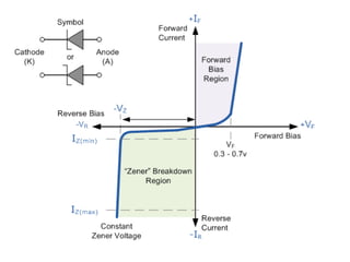
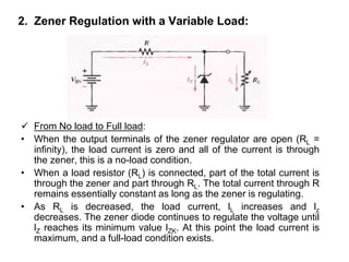
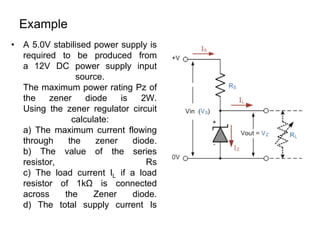
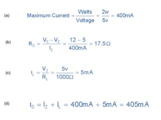
Zener Diode
• The Zener diode is like a general-purpose diode consisting of a
silicon PN junction.
• When biased in the forward direction it behaves just like a normal
diode passing the rated current,
• When a reverse voltage is applied to it the reverse current remains
fairly constant over a wide range of voltages
• The reverse voltage increases until the diodes breakdown voltage
VBR is reached at which point, Breakdown occurs in the depletion
layer and the current flowing through the zener diode increases
dramatically to the maximum circuit value (which is usually limited
by a series resistor).
• This breakdown voltage point is called the "zener voltage" for
zener diodes
• The point at which current flows can be very accurately controlled
(to less than 1% tolerance) in the doping stage of the diodes
construction giving the diode a specific zener breakdown voltage,
(Vz) ranging from a few volts up to a few hundred volts.
• This zener breakdown voltage on the I-V curve is almost a vertical
straight line
• The Zener Diode is used in its "reverse bias" or reverse breakdown
mode, i.e. the diodes anode connects to the negative supply.
• From the I-V characteristics curve, it can be seen that the zener
diode has a region in its reverse bias characteristics of almost a
constant negative voltage regardless of the value of the current
flowing through the diode and remains nearly constant even with
large changes in current as long as the zener diodes current
remains between the breakdown current IZ(min) and the maximum
current rating IZ(max).
• This ability to control itself can be used to great effect to regulate or
stabilise a voltage source against supply or load variations.
• The fact that the voltage across the diode in the breakdown region is
almost constant turns out to be an important application of the zener
diode as a voltage regulator.
• The function of a regulator is to provide a constant output voltage to
a load connected in parallel with it in spite of the ripples in the
supply voltage or the variation in the load current and the zener
diode will continue to regulate the voltage until the diodes current
falls below the minimum IZ(min value in the reverse breakdown
region.
Zener Breakdown
• Zener diodes are designed to operate in reverse breakdown.
• Two types of reverse breakdown in a zener diode are
– avalanche and zener.
• The avalanche breakdown occurs in both rectifier and zener diodes
at a sufficiently high reverse voltage.
• Zener breakdown occurs in a zener diode at low reverse voltages.
• A zener diode is heavily doped to reduce the breakdown voltage,
which causes a very thin depletion region.
• As a result, an intense electric field exists within the depletion
region.
• Near the zener breakdown voltage (Vz ), the field is intense enough
to pull electrons from their valence bands and create current,
• Zener diodes with breakdown voltages of less than approximately 5
V operate predominately in zener breakdown.
• Those with breakdown voltages greater than approximately 5 V
operate predominately in avalanche breakdown.
• Zeners are commercially available with breakdown voltages of 1.8 V
to 200 V with specified tolerances from I% to 20%.
Breakdown Characteristics
• Figure shows the reverse portion
of a zener diode's characteristic
curve,
• The reverse voltage (VR) is
increased, the reverse current (IR)
remains extremely small up to the
"knee" of the curve.
• The reverse current is also called
the zener current (lz).
• At this point, the breakdown
effect begins: the internal zener
resistance, also called zener
impedance (Zz), begins to
decrease as the reverse current
increases rapidly.
• From the bottom of the knee. the
zener breakdown voltage (Vz)
remains essentially constant
although it increases slightly as
the zener current (lz) increase.
Zener Regulation
• The ability to keep the reverse voltage across its terminals
essentially constant is the key feature of the zener diode.
• A zener diode operating in breakdown acts as a voltage regulator
because it maintains a nearly constant voltage across its
terminals over a specified range of reverse-current values.
• A minimum value of reverse current, IZK must he maintained in
order to keep the diode in breakdown for voltage regulation.
• It can be seem on the curve that when the reverse current is
reduced below the knee of the curve, the voltage decreases
drastically and regulation is lost.
• Also, there is a maximum current, IZM above which the diode may
be damaged due to excessive power dissipation.
• So, basically. the zener diode maintains a nearly constant
voltage across its terminals for values of reverse current ranging
from IZK to to IZM
• A nominal zener voltage, VZT , is usually specified on a data
sheet at a value of reverse current called the zener test current,
lZT
Zener Equivalent Circuit
• Figure shows the ideal
model of a zener diode in
reverse breakdown. It has a
constant voltage drop equal
to the nominal zener
voltage.
• This constant voltage drop
is represented by a dc
voltage source even though
the zener diode does not
actually produce an emf
voltage.
• The dc source simply
indicates that the effect of
reverse breakdown is a
constant voltage across the
zener terminals.
• Figure represents the practical
model of a zener diode, where
the zener impedance (Zz) is
included.
• Since the actual voltage curve
is not ideally vertical, a change
in zener current (Δlz) produces
a small change in zener
voltage (ΔVz).
• By Ohm's law, Zz = ΔVz / Δlz
• Normally, Zz is specified at IZT,
the zener test current, and is
designated ZZT
• In most cases, it can be
assumed that Zz is constant
over the full linear range of
zener current values and is
purely resistive.
A zener diode exhibits a certain change in V z for a certain
change in lz on a portion of the linear characteristic curve
between IZK and IZM as illustrated in Figure. What is the zener
impedance?
A zener diode has a ZZT of 3.5 Ω. The data sheet gives VZT
= 6.8 V at IZT = 37 mA and IZK = 1 mA. What is the voltage
across the zener terminals when the current is 50 mA?
When the cunent is 25 mA?
Temperature Coefficient
• The temperature coefficient specifies the percent change
in zener voltage for each degree centigrade change in
temperature.
• For example, a 12 V zener diode with a positive
temperature coefficient of 0.01% /OC will exhibit a 1.2
mV increase in Vz when the junction temperature
increases one degree centigrade.
• The formula for calculating the change in zener voltage
for a given junction temperature change, for a specified
temperature coefficient, is
Where Vz is nominal zener voltage at 250C
When temp. coefficient is expressed in mV/0C
Zener Power Dissipation
• Zener diodes are specified to operate at a maximum
power called the maximum dc power dissipation, PD(max).
• For example, the lN746 zener is rated at a PD(max) of 500
mW and the IN3305A is rated at a PD(max) of 50 W.
• The dc power dissipation is determined by the formula,
• PD = VZ IZ
Power Derating
• The maximum power dissipation of a zener
diode is typically specified for temperatures at or
below a certain value (50°C, for example).
• Above the specified temperature. the maximum
power dissipation is reduced according to a
derating factor.
• The derating factor is expressed in mW/°C.
• The maximum derated power can be determined
with the following formula:
Zener Diode Applications
1. Zener Regulation with a Varying Input Voltage:
2. Zener Regulation with a Variable Load:
 From No load to Full load:
• When the output terminals of the zener regulator are open (RL =
infinity), the load current is zero and all of the current is through
the zener, this is a no-load condition.
• When a load resistor (RL) is connected, part of the total current is
through the zener and part through RL. The total current through R
remains essentially constant as long as the zener is regulating.
• As RL is decreased, the load current, lL increases and lz
decreases. The zener diode continues to regulate the voltage until
lZ reaches its minimum value lZK. At this point the load current is
maximum, and a full-load condition exists.
3. Zener Limiting:
Example
• A 5.0V stabilised power supply is
required to be produced from
a 12V DC power supply input
source.
The maximum power rating Pz of
the zener diode is 2W.
Using the zener regulator circuit
calculate:
a) The maximum current flowing
through the zener diode.
b) The value of the series
resistor, Rs
c) The load current IL if a load
resistor of 1kΩ is connected
across the Zener diode.
d) The total supply current Is
(a)
(b)
(c)
(d)
Zener Diode Voltages
• As well as producing a single stabilised voltage
output, zener diodes can also be connected
together in series along with normal silicon
signal diodes to produce a variety of different
reference voltage output values
• The values of the individual Zener diodes can be
chosen to suit the application while the silicon
diode will always drop about 0.6 - 0.7V in the
forward bias condition.
• The supply voltage, Vin must of course be higher
than the largest output reference voltage
Zener Diode Standard Voltages
BZX55 Zener Diode Power Rating 500mW
2.4V 2.7V 3.0V 3.3V 3.6V 3.9V 4.3V 4.7V
5.1V 5.6V 6.2V 6.8V 7.5V 8.2V 9.1V 10V
11V 12V 13V 15V 16V 18V 20V 22V
24V 27V 30V 33V 36V 39V 43V 47V
BZX85 Zener Diode Power Rating 1.3W
3.3V 3.6V 3.9V 4.3V 4.7V 5.1V 5.6 6.2V
6.8V 7.5V 8.2V 9.1V 10V 11V 12V 13V
15V 16V 18V 20V 22V 24V 27V 30V
33V 36V 39V 43V 47V 51V 56V 62V
Summary
• A zener diode is always operated in its reverse biased
condition.
• A voltage regulator circuit can be designed using a zener
diode to maintain a constant DC output voltage across
the load in spite of variations in the input voltage or
changes in the load current.
• The zener voltage regulator consists of a current limiting
resistor Rs connected in series with the input voltage Vs
with the zener diode connected in parallel with the load
RL in this reverse biased condition.
• The stabilized output voltage is always selected to be the
same as the breakdown voltage Vz of the diode.

Zener Diodes.ppt

  • 1.
  • 2.
    • The Zenerdiode is like a general-purpose diode consisting of a silicon PN junction. • When biased in the forward direction it behaves just like a normal diode passing the rated current, • When a reverse voltage is applied to it the reverse current remains fairly constant over a wide range of voltages • The reverse voltage increases until the diodes breakdown voltage VBR is reached at which point, Breakdown occurs in the depletion layer and the current flowing through the zener diode increases dramatically to the maximum circuit value (which is usually limited by a series resistor). • This breakdown voltage point is called the "zener voltage" for zener diodes • The point at which current flows can be very accurately controlled (to less than 1% tolerance) in the doping stage of the diodes construction giving the diode a specific zener breakdown voltage, (Vz) ranging from a few volts up to a few hundred volts. • This zener breakdown voltage on the I-V curve is almost a vertical straight line
  • 4.
    • The ZenerDiode is used in its "reverse bias" or reverse breakdown mode, i.e. the diodes anode connects to the negative supply. • From the I-V characteristics curve, it can be seen that the zener diode has a region in its reverse bias characteristics of almost a constant negative voltage regardless of the value of the current flowing through the diode and remains nearly constant even with large changes in current as long as the zener diodes current remains between the breakdown current IZ(min) and the maximum current rating IZ(max). • This ability to control itself can be used to great effect to regulate or stabilise a voltage source against supply or load variations. • The fact that the voltage across the diode in the breakdown region is almost constant turns out to be an important application of the zener diode as a voltage regulator. • The function of a regulator is to provide a constant output voltage to a load connected in parallel with it in spite of the ripples in the supply voltage or the variation in the load current and the zener diode will continue to regulate the voltage until the diodes current falls below the minimum IZ(min value in the reverse breakdown region.
  • 6.
    Zener Breakdown • Zenerdiodes are designed to operate in reverse breakdown. • Two types of reverse breakdown in a zener diode are – avalanche and zener. • The avalanche breakdown occurs in both rectifier and zener diodes at a sufficiently high reverse voltage. • Zener breakdown occurs in a zener diode at low reverse voltages. • A zener diode is heavily doped to reduce the breakdown voltage, which causes a very thin depletion region. • As a result, an intense electric field exists within the depletion region. • Near the zener breakdown voltage (Vz ), the field is intense enough to pull electrons from their valence bands and create current, • Zener diodes with breakdown voltages of less than approximately 5 V operate predominately in zener breakdown. • Those with breakdown voltages greater than approximately 5 V operate predominately in avalanche breakdown. • Zeners are commercially available with breakdown voltages of 1.8 V to 200 V with specified tolerances from I% to 20%.
  • 7.
    Breakdown Characteristics • Figureshows the reverse portion of a zener diode's characteristic curve, • The reverse voltage (VR) is increased, the reverse current (IR) remains extremely small up to the "knee" of the curve. • The reverse current is also called the zener current (lz). • At this point, the breakdown effect begins: the internal zener resistance, also called zener impedance (Zz), begins to decrease as the reverse current increases rapidly. • From the bottom of the knee. the zener breakdown voltage (Vz) remains essentially constant although it increases slightly as the zener current (lz) increase.
  • 8.
    Zener Regulation • Theability to keep the reverse voltage across its terminals essentially constant is the key feature of the zener diode. • A zener diode operating in breakdown acts as a voltage regulator because it maintains a nearly constant voltage across its terminals over a specified range of reverse-current values. • A minimum value of reverse current, IZK must he maintained in order to keep the diode in breakdown for voltage regulation. • It can be seem on the curve that when the reverse current is reduced below the knee of the curve, the voltage decreases drastically and regulation is lost. • Also, there is a maximum current, IZM above which the diode may be damaged due to excessive power dissipation. • So, basically. the zener diode maintains a nearly constant voltage across its terminals for values of reverse current ranging from IZK to to IZM • A nominal zener voltage, VZT , is usually specified on a data sheet at a value of reverse current called the zener test current, lZT
  • 9.
    Zener Equivalent Circuit •Figure shows the ideal model of a zener diode in reverse breakdown. It has a constant voltage drop equal to the nominal zener voltage. • This constant voltage drop is represented by a dc voltage source even though the zener diode does not actually produce an emf voltage. • The dc source simply indicates that the effect of reverse breakdown is a constant voltage across the zener terminals.
  • 10.
    • Figure representsthe practical model of a zener diode, where the zener impedance (Zz) is included. • Since the actual voltage curve is not ideally vertical, a change in zener current (Δlz) produces a small change in zener voltage (ΔVz). • By Ohm's law, Zz = ΔVz / Δlz • Normally, Zz is specified at IZT, the zener test current, and is designated ZZT • In most cases, it can be assumed that Zz is constant over the full linear range of zener current values and is purely resistive.
  • 12.
    A zener diodeexhibits a certain change in V z for a certain change in lz on a portion of the linear characteristic curve between IZK and IZM as illustrated in Figure. What is the zener impedance?
  • 13.
    A zener diodehas a ZZT of 3.5 Ω. The data sheet gives VZT = 6.8 V at IZT = 37 mA and IZK = 1 mA. What is the voltage across the zener terminals when the current is 50 mA? When the cunent is 25 mA?
  • 14.
    Temperature Coefficient • Thetemperature coefficient specifies the percent change in zener voltage for each degree centigrade change in temperature. • For example, a 12 V zener diode with a positive temperature coefficient of 0.01% /OC will exhibit a 1.2 mV increase in Vz when the junction temperature increases one degree centigrade. • The formula for calculating the change in zener voltage for a given junction temperature change, for a specified temperature coefficient, is Where Vz is nominal zener voltage at 250C When temp. coefficient is expressed in mV/0C
  • 16.
    Zener Power Dissipation •Zener diodes are specified to operate at a maximum power called the maximum dc power dissipation, PD(max). • For example, the lN746 zener is rated at a PD(max) of 500 mW and the IN3305A is rated at a PD(max) of 50 W. • The dc power dissipation is determined by the formula, • PD = VZ IZ
  • 17.
    Power Derating • Themaximum power dissipation of a zener diode is typically specified for temperatures at or below a certain value (50°C, for example). • Above the specified temperature. the maximum power dissipation is reduced according to a derating factor. • The derating factor is expressed in mW/°C. • The maximum derated power can be determined with the following formula:
  • 19.
    Zener Diode Applications 1.Zener Regulation with a Varying Input Voltage:
  • 21.
    2. Zener Regulationwith a Variable Load:  From No load to Full load: • When the output terminals of the zener regulator are open (RL = infinity), the load current is zero and all of the current is through the zener, this is a no-load condition. • When a load resistor (RL) is connected, part of the total current is through the zener and part through RL. The total current through R remains essentially constant as long as the zener is regulating. • As RL is decreased, the load current, lL increases and lz decreases. The zener diode continues to regulate the voltage until lZ reaches its minimum value lZK. At this point the load current is maximum, and a full-load condition exists.
  • 22.
  • 23.
    Example • A 5.0Vstabilised power supply is required to be produced from a 12V DC power supply input source. The maximum power rating Pz of the zener diode is 2W. Using the zener regulator circuit calculate: a) The maximum current flowing through the zener diode. b) The value of the series resistor, Rs c) The load current IL if a load resistor of 1kΩ is connected across the Zener diode. d) The total supply current Is
  • 24.
  • 25.
    Zener Diode Voltages •As well as producing a single stabilised voltage output, zener diodes can also be connected together in series along with normal silicon signal diodes to produce a variety of different reference voltage output values • The values of the individual Zener diodes can be chosen to suit the application while the silicon diode will always drop about 0.6 - 0.7V in the forward bias condition. • The supply voltage, Vin must of course be higher than the largest output reference voltage
  • 27.
    Zener Diode StandardVoltages BZX55 Zener Diode Power Rating 500mW 2.4V 2.7V 3.0V 3.3V 3.6V 3.9V 4.3V 4.7V 5.1V 5.6V 6.2V 6.8V 7.5V 8.2V 9.1V 10V 11V 12V 13V 15V 16V 18V 20V 22V 24V 27V 30V 33V 36V 39V 43V 47V BZX85 Zener Diode Power Rating 1.3W 3.3V 3.6V 3.9V 4.3V 4.7V 5.1V 5.6 6.2V 6.8V 7.5V 8.2V 9.1V 10V 11V 12V 13V 15V 16V 18V 20V 22V 24V 27V 30V 33V 36V 39V 43V 47V 51V 56V 62V
  • 28.
    Summary • A zenerdiode is always operated in its reverse biased condition. • A voltage regulator circuit can be designed using a zener diode to maintain a constant DC output voltage across the load in spite of variations in the input voltage or changes in the load current. • The zener voltage regulator consists of a current limiting resistor Rs connected in series with the input voltage Vs with the zener diode connected in parallel with the load RL in this reverse biased condition. • The stabilized output voltage is always selected to be the same as the breakdown voltage Vz of the diode.