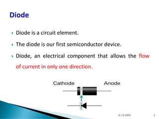
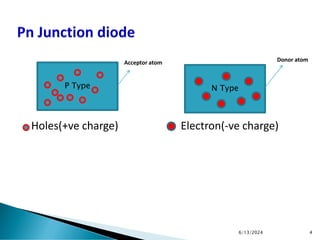
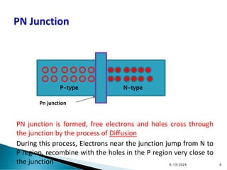
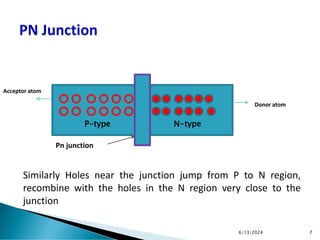
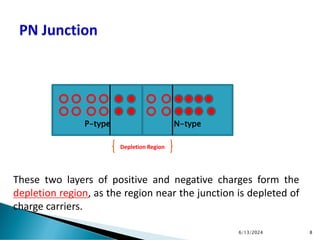
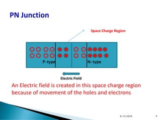
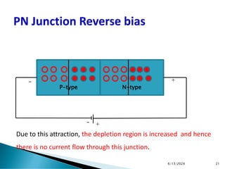
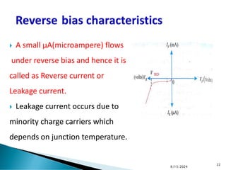
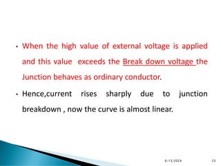
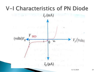
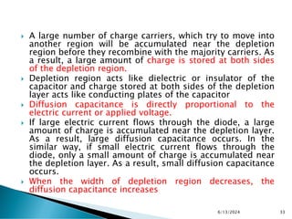
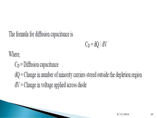
By
Ms.J.Shiny Christobel
Assistant Professor/ ECE
Sri Ramakrishna Institute of Technology, Coimbatore
1
 Diode is a circuit element.
 The diode is our first semiconductor device.
 Diode, an electrical component that allows the flow
of current in only one direction.
6/13/2024 2
 PN Junction Diode
 Zener Diode
6/13/2024 3
Holes(+ve charge) Electron(-ve charge)
P Type N Type
Acceptor atom Donor atom
6/13/2024 4
 When a p-type semiconductor is suitably joined to n-type
semiconductor, the contact surface is called pn junction.
 Most semiconductor devices contain one or more pn
junction.
 In pn junction consists of two types of materials. They are
p-type and n-type.
 The p-type material has holes while the n-type material has
free electrons.
6/13/2024 5
PN junction is formed, free electrons and holes cross through
the junction by the process of Diffusion
During this process, Electrons near the junction jump from N to
P region, recombine with the holes in the P region very close to
the junction
P-type N-type
Pn junction
6/13/2024 6
Similarly Holes near the junction jump from P to N region,
recombine with the holes in the N region very close to the
junction
P-type N-type
Pn junction
Donor atom
Acceptor atom
6/13/2024 7
P-type N-type
6/13/2024 8
Depletion Region
These two layers of positive and negative charges form the
depletion region, as the region near the junction is depleted of
charge carriers.
Electric Field
An Electric field is created in this space charge region
because of movement of the holes and electrons
P-type N-type
6/13/2024 9
Space Charge Region
 An electric field is setup, between donor and acceptor
ions in the depletion region
 The potential at the N-side is higher then the potential
at P-side.
 Therefore, electrons in the N-side are prevented to go
to the lower potential of P-side
 Similarly, holes in the P-side find themselves at a lower
potential and are prevented to cross to the N-side
6/13/2024 10
Electric Field
P-type N-type
6/13/2024 11
Space Charge Region
Depletion Region
 The electric field formed in the depletion region acts as
a barrier.
 External energy must be applied to get the electrons to
move across the barrier of the electric field.
 The potential difference required to move the
electrons through the electric field is called the barrier
potential.
 Barrier potential of a PN junction depends on the type
of semiconductor material, amount of doping and
temperature.
 This is approximately 0.7V for silicon and 0.3V for
germanium. 6/13/2024 12
Positive terminal of Negative terminal of
battery to P region battery to N region
P-type N-type
6/13/2024 13
+
_
Positive terminal
Repels the holes
P-type N-type
6/13/2024 14
+
_
Negative terminal Repels the electrons
towards the junction
Due to this repulsion, the depletion region disappears and also potential
barrier also disappears.
Hence under this action of the forward potential difference, the majority
charge carriers flow across the junction in opposite direction and
constitute current flow in the forward direction. This is called Forward
current IF
P-type N-type
6/13/2024 15
+
_
• Current increase very slowly with
respect to voltage. The curve is
nonlinear.
• When the external voltage exceeds the
potential barrier voltage the Junction
behaves as ordinary conductor.
• Hence,current rises sharply with
increase in external voltage, now the
curve is almost linear.
6/13/2024 16
P-type N-type
6/13/2024 17
_
+
Battery is connected with negative terminal to N region and positive
terminal to P region
Holes get attracted to the negative terminal of the battery
P-type N-type
6/13/2024 18
_
+
+
_
Electrons get attracted to the Positive terminal of the battery
P-type N-type
6/13/2024 19
_
+
+
_
This results in the increase of the depletion region
P-type N-type
6/13/2024 20
_
+
+
_
Due to this attraction, the depletion region is increased and hence
there is no current flow through this junction.
P-type N-type
6/13/2024 21
_
+
+
_
6/13/2024
22
 A small µA(microampere) flows
under reverse bias and hence it is
called as Reverse current or
Leakage current.
 Leakage current occurs due to
minority charge carriers which
depends on junction temperature.
• When the high value of external voltage is applied
and this value exceeds the Break down voltage the
Junction behaves as ordinary conductor.
• Hence,current rises sharply due to junction
breakdown , now the curve is almost linear.
6/13/2024 23
6/13/2024 24
VB
Basic operation of a capacitor:
 Capacitors store electric charge in the form of electric field. This
charge storage is done by using two electrically conducting plates
(placed close to each other) separated by an insulating material
called dielectric.
 The conducting plates or electrodes of the capacitor are good
conductors of electricity. Therefore, they easily allow electric current
through them. On the other hand, dielectric material or medium is
poor conductor of electricity. Therefore, it does not allow electric
current through it. However, it efficiently allows electric field.
 When voltage is applied to the capacitor, charge carriers starts
flowing through the conducting wire.
 When these charge carriers reach the electrodes of the capacitor,
they experience a strong opposition from the dielectric or insulating
material. As a result, a large number of charge carriers are trapped
at the electrodes of the capacitor. These charge carriers cannot
move between the plates. However, they exerts electric field
between the plates. The charge carriers which are trapped near the
dielectric material will stores electric charge. The ability of the
material to store electric charge is called capacitance.
6/13/2024 25
6/13/2024 26
In a basic capacitor, the capacitance is directly proportional to
the size of electrodes or plates and inversely proportional to the
distance between two plates
 In a p-n junction diode, two types of capacitance take
place. They are,
Transition capacitance (CT)
Diffusion capacitance (CD)
a) Transition capacitance (CT):
 Just like the capacitors, a reverse biased p-n junction
diode also stores electric charge at the depletion
region
 p-type and n-type regions act like the electrodes or
conducting plates of the capacitor. The depletion
region of the p-n junction diode has high resistance.
Hence, the depletion region acts like the dielectric or
insulating material
 Therefore, charge is stored at the depletion region in
the form of electric field. The ability of a material to
store electric charge is called capacitance. Thus,there
exists a capacitance at the depletion region.
6/13/2024 27
6/13/2024 28
 The p-n junction diode with narrow depletion width and
large p-type and n-type regions will store large amount of
electric charge whereas the pn junction diode with wide
depletion width and small p-type and n-type regions will
store only a small amount of electric charge. Therefore,
the capacitance of the reverse bias p-n junction diode
decreases when voltage increases.
 In a forward biased diode, the transition capacitance exist.
However, the transition capacitance is very small
compared to the diffusion capacitance. Hence, transition
capacitance is neglected in forward biased diode.
 The amount of capacitance changed with increase in
voltage is called transition capacitance. The transition
capacitance is also known as depletion region
capacitance, junction capacitance or barrier capacitance.
 Transition capacitance is denoted as CT.
6/13/2024 29
6/13/2024 30
Diffusion capacitance (CD):
 Diffusion capacitance occurs in a forward biased
p-n junction diode. Diffusion capacitance is also
sometimes referred as storage capacitance. It is
denoted as CD.
 In a forward biased diode, diffusion capacitance
is much larger than the transition capacitance.
Hence, diffusion capacitance is considered in
forward biased diode.
 The diffusion capacitance occurs due to stored
charge of minority electrons and minority holes
near the depletion region.
6/13/2024 31
 A large number of charge carriers, which try to move into
another region will be accumulated near the depletion region
before they recombine with the majority carriers. As a result,
a large amount of charge is stored at both sides of the
depletion region.
6/13/2024 32
 A large number of charge carriers, which try to move into
another region will be accumulated near the depletion
region before they recombine with the majority carriers. As
a result, a large amount of charge is stored at both sides
of the depletion region.
 Depletion region acts like dielectric or insulator of the
capacitor and charge stored at both sides of the depletion
layer acts like conducting plates of the capacitor
 Diffusion capacitance is directly proportional to the
electric current or applied voltage.
 If large electric current flows through the diode, a large
amount of charge is accumulated near the depletion layer.
As a result, large diffusion capacitance occurs. In the
similar way, if small electric current flows through the
diode, only a small amount of charge is accumulated near
the depletion layer. As a result, small diffusion capacitance
occurs.
 When the width of depletion region decreases, the
diffusion capacitance increases
6/13/2024 33
6/13/2024 34

PN Junction Diode and its V - I Characteristics

  • 1.
    By Ms.J.Shiny Christobel Assistant Professor/ECE Sri Ramakrishna Institute of Technology, Coimbatore 1
  • 2.
     Diode isa circuit element.  The diode is our first semiconductor device.  Diode, an electrical component that allows the flow of current in only one direction. 6/13/2024 2
  • 3.
     PN JunctionDiode  Zener Diode 6/13/2024 3
  • 4.
    Holes(+ve charge) Electron(-vecharge) P Type N Type Acceptor atom Donor atom 6/13/2024 4
  • 5.
     When ap-type semiconductor is suitably joined to n-type semiconductor, the contact surface is called pn junction.  Most semiconductor devices contain one or more pn junction.  In pn junction consists of two types of materials. They are p-type and n-type.  The p-type material has holes while the n-type material has free electrons. 6/13/2024 5
  • 6.
    PN junction isformed, free electrons and holes cross through the junction by the process of Diffusion During this process, Electrons near the junction jump from N to P region, recombine with the holes in the P region very close to the junction P-type N-type Pn junction 6/13/2024 6
  • 7.
    Similarly Holes nearthe junction jump from P to N region, recombine with the holes in the N region very close to the junction P-type N-type Pn junction Donor atom Acceptor atom 6/13/2024 7
  • 8.
    P-type N-type 6/13/2024 8 DepletionRegion These two layers of positive and negative charges form the depletion region, as the region near the junction is depleted of charge carriers.
  • 9.
    Electric Field An Electricfield is created in this space charge region because of movement of the holes and electrons P-type N-type 6/13/2024 9 Space Charge Region
  • 10.
     An electricfield is setup, between donor and acceptor ions in the depletion region  The potential at the N-side is higher then the potential at P-side.  Therefore, electrons in the N-side are prevented to go to the lower potential of P-side  Similarly, holes in the P-side find themselves at a lower potential and are prevented to cross to the N-side 6/13/2024 10
  • 11.
    Electric Field P-type N-type 6/13/202411 Space Charge Region Depletion Region
  • 12.
     The electricfield formed in the depletion region acts as a barrier.  External energy must be applied to get the electrons to move across the barrier of the electric field.  The potential difference required to move the electrons through the electric field is called the barrier potential.  Barrier potential of a PN junction depends on the type of semiconductor material, amount of doping and temperature.  This is approximately 0.7V for silicon and 0.3V for germanium. 6/13/2024 12
  • 13.
    Positive terminal ofNegative terminal of battery to P region battery to N region P-type N-type 6/13/2024 13 + _
  • 14.
    Positive terminal Repels theholes P-type N-type 6/13/2024 14 + _ Negative terminal Repels the electrons towards the junction
  • 15.
    Due to thisrepulsion, the depletion region disappears and also potential barrier also disappears. Hence under this action of the forward potential difference, the majority charge carriers flow across the junction in opposite direction and constitute current flow in the forward direction. This is called Forward current IF P-type N-type 6/13/2024 15 + _
  • 16.
    • Current increasevery slowly with respect to voltage. The curve is nonlinear. • When the external voltage exceeds the potential barrier voltage the Junction behaves as ordinary conductor. • Hence,current rises sharply with increase in external voltage, now the curve is almost linear. 6/13/2024 16
  • 17.
    P-type N-type 6/13/2024 17 _ + Batteryis connected with negative terminal to N region and positive terminal to P region
  • 18.
    Holes get attractedto the negative terminal of the battery P-type N-type 6/13/2024 18 _ + + _
  • 19.
    Electrons get attractedto the Positive terminal of the battery P-type N-type 6/13/2024 19 _ + + _
  • 20.
    This results inthe increase of the depletion region P-type N-type 6/13/2024 20 _ + + _
  • 21.
    Due to thisattraction, the depletion region is increased and hence there is no current flow through this junction. P-type N-type 6/13/2024 21 _ + + _
  • 22.
    6/13/2024 22  A smallµA(microampere) flows under reverse bias and hence it is called as Reverse current or Leakage current.  Leakage current occurs due to minority charge carriers which depends on junction temperature.
  • 23.
    • When thehigh value of external voltage is applied and this value exceeds the Break down voltage the Junction behaves as ordinary conductor. • Hence,current rises sharply due to junction breakdown , now the curve is almost linear. 6/13/2024 23
  • 24.
  • 25.
    Basic operation ofa capacitor:  Capacitors store electric charge in the form of electric field. This charge storage is done by using two electrically conducting plates (placed close to each other) separated by an insulating material called dielectric.  The conducting plates or electrodes of the capacitor are good conductors of electricity. Therefore, they easily allow electric current through them. On the other hand, dielectric material or medium is poor conductor of electricity. Therefore, it does not allow electric current through it. However, it efficiently allows electric field.  When voltage is applied to the capacitor, charge carriers starts flowing through the conducting wire.  When these charge carriers reach the electrodes of the capacitor, they experience a strong opposition from the dielectric or insulating material. As a result, a large number of charge carriers are trapped at the electrodes of the capacitor. These charge carriers cannot move between the plates. However, they exerts electric field between the plates. The charge carriers which are trapped near the dielectric material will stores electric charge. The ability of the material to store electric charge is called capacitance. 6/13/2024 25
  • 26.
    6/13/2024 26 In abasic capacitor, the capacitance is directly proportional to the size of electrodes or plates and inversely proportional to the distance between two plates
  • 27.
     In ap-n junction diode, two types of capacitance take place. They are, Transition capacitance (CT) Diffusion capacitance (CD) a) Transition capacitance (CT):  Just like the capacitors, a reverse biased p-n junction diode also stores electric charge at the depletion region  p-type and n-type regions act like the electrodes or conducting plates of the capacitor. The depletion region of the p-n junction diode has high resistance. Hence, the depletion region acts like the dielectric or insulating material  Therefore, charge is stored at the depletion region in the form of electric field. The ability of a material to store electric charge is called capacitance. Thus,there exists a capacitance at the depletion region. 6/13/2024 27
  • 28.
  • 29.
     The p-njunction diode with narrow depletion width and large p-type and n-type regions will store large amount of electric charge whereas the pn junction diode with wide depletion width and small p-type and n-type regions will store only a small amount of electric charge. Therefore, the capacitance of the reverse bias p-n junction diode decreases when voltage increases.  In a forward biased diode, the transition capacitance exist. However, the transition capacitance is very small compared to the diffusion capacitance. Hence, transition capacitance is neglected in forward biased diode.  The amount of capacitance changed with increase in voltage is called transition capacitance. The transition capacitance is also known as depletion region capacitance, junction capacitance or barrier capacitance.  Transition capacitance is denoted as CT. 6/13/2024 29
  • 30.
  • 31.
    Diffusion capacitance (CD): Diffusion capacitance occurs in a forward biased p-n junction diode. Diffusion capacitance is also sometimes referred as storage capacitance. It is denoted as CD.  In a forward biased diode, diffusion capacitance is much larger than the transition capacitance. Hence, diffusion capacitance is considered in forward biased diode.  The diffusion capacitance occurs due to stored charge of minority electrons and minority holes near the depletion region. 6/13/2024 31
  • 32.
     A largenumber of charge carriers, which try to move into another region will be accumulated near the depletion region before they recombine with the majority carriers. As a result, a large amount of charge is stored at both sides of the depletion region. 6/13/2024 32
  • 33.
     A largenumber of charge carriers, which try to move into another region will be accumulated near the depletion region before they recombine with the majority carriers. As a result, a large amount of charge is stored at both sides of the depletion region.  Depletion region acts like dielectric or insulator of the capacitor and charge stored at both sides of the depletion layer acts like conducting plates of the capacitor  Diffusion capacitance is directly proportional to the electric current or applied voltage.  If large electric current flows through the diode, a large amount of charge is accumulated near the depletion layer. As a result, large diffusion capacitance occurs. In the similar way, if small electric current flows through the diode, only a small amount of charge is accumulated near the depletion layer. As a result, small diffusion capacitance occurs.  When the width of depletion region decreases, the diffusion capacitance increases 6/13/2024 33
  • 34.