
Recommended
More Related Content
What's hot
Viewers also liked
Viewers also liked (14)
Similar to ArvindP1
Similar to ArvindP1 (20)
ArvindP1
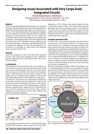
- 1. IJCST Vol. 4, Issue 2, April - June 2013 ISSN : 0976-8491 (Online) | ISSN : 2229-4333 (Print) w w w.ijcst.com92 International Journal of Computer Science And Technology Designing Issues Associated with Very Large Scale Integrated Circuits 1 Arvind Singh Rawat, 2 Amit Kumar 1 Uttarkhand Technical University, Dehradun, UK, India 2 SSGI Shahpur, Yamunanagar, Haryana, India Abstract TheVery Large Scale Integration orVLSI is the process of placing thousands or hundreds of thousands of electronic components on a single chip. Nearly all modern chips employVLSI architectures or ULSIi.e.UltraLargeScaleIntegration.Very-large-scaleintegration (VLSI) is the process of creating integrated circuits by combining thousands of transistor-based circuits into on a single chip. VLSI began when complex semiconductor and communication technologies were being developed.The first semiconductor chips held one transistor each. Subsequent advances added more and more transistors, and as a consequence more individual functions or systems were integrated over time. The microprocessor is a VLSI device. In this paper we mainly focus on the designing issues associated with the VLSI. Keyword Small Scale Integrated Circuits, Very Large Scale Integrated Circuits, Ultra Large Scale Integrated Circuits, Application Specific Integrated Circuits, Field Programmable Gate Arrays, System On Chips. I. Introduction The development of microelectronics spans a time which is even lesser than the average life expectancy of a human, and yet it has seen as many as four generations. Early 60’s saw the low density fabrication processes classified under Small Scale Integration (SSI) in which transistor count was limited to about 10. This rapidly gave way to Medium Scale Integration in the late 60’s when around 100 transistors could be placed on a single chip. It was the time when the cost of research began to decline and private firms started entering the competition in contrast to the earlier years where the main burden was borne by the military. Transistor-Transistor logic (TTL) offering higher integration densities outlasted other IC families like ECL and became the basis of the first integrated circuit revolution. Early seventies marked the growth of transistor count to about 1000 per chip called the Large Scale Integration. Fig. 1: Moore’s Law & IC’s By mid eighties, the transistor count on a single chip had already exceeded 1000 and hence came the age of Very Large Scale Integration or VLSI. Though many improvements have been made and the transistor count is still rising, further names of generations like ULSI are generally avoided. It was during this time when TTL lost the battle to MOS family owing to the same problems that had pushed vacuum tubes into negligence, power dissipation and the limit it imposed on the number of gates that could be placed on a single die. II. Factors Involved in VLSI In VLSI circuits it takes less power because each of the devices consumes only a tiny amount of power. In a switching circuit most of the power is consumed switching the charge on the capacitors that connect the switches to each other. In a large IC the components are so small and close together that that capacitance is much smaller and thus less power. It also supports less testing. If youbuiltthesamecircuitoutofdiscreteICsandothercomponents, each IC has to be tested before you use it for the many different ways it could be used in different applications. For 10000 ICs this is a lot of testing. In a VLSI the components are dedicated to a single use. Most are located in the middle of the VLSI and there is no access to them for testing. We can only test the function; the entire circuit was designed for. Normally, VLSI circuits are highly reliable. The reliability of an IC is a function depends on of how many connections it has to the outside world. So if the function is constructed with many smaller ICs connected together, then there are many connections, and the reliability is lower. Those VLSI that have fewer connections should be higher reliability. Small transistor count precision circuits such asAmplifiers, Data converters, filters, Phase Locked Loops, Sensors etc. Fig. 2: Integrated Circuit Industry Impact
- 2. IJCST Vol. 4, Issue 2, April - June 2013 w w w.ijcst.com International Journal of Computer Science And Technology 93 ISSN : 0976-8491 (Online) | ISSN : 2229-4333 (Print) VLSI's design tools eventually included not only design entry and simulation but eventually cell-based routing or chip compiler, a data-path compiler, SRAM and ROM compilers, and a state machine compiler. The tools were an integrated design solution for IC design and not just point tools, or more general purpose system tools. A designer could edit transistor-level polygons or logic schematics, then run DRC and LVS, extract parasitic from the layout and run Spice simulation, then back-annotate the timing or gate size changes into the logic schematic database. VLSI's physical design tools were critical not only to its ASIC business, but also in setting the bar for the commercial EDAindustry.When VLSI and its mainASIC competitor, LSI Logic, were establishing theASIC industry, commercially-available tools could not deliver the productivity necessary to support the physical design of hundreds of ASIC designs each year without the deployment of a substantial number of layout engineers. Unfortunately, for all VLSI's initial competence in design tools, they were not leaders in semiconductor manufacturing technology. VLSI had not been timely in developing a 1.0 μm manufacturing process as the rest of the industry moved to that geometry in the late 80s. The VLSI entered the merchant high speed static RAM (SRAM) market as they needed a product to drive the semiconductor process technology development. All the large semiconductor companies built high speed SRAMs with cost structures VLSI could never match. The first "generation" of computers relied on vacuum tubes. Then came discrete semiconductor devices, followed by integrated circuits. The first Small-Scale Integration (SSI) ICs had small numbers of devices on a single chip diodes, transistors, resistors and capacitors i.e. no inductors though, making it possible to fabricate one or more logic gates on a single device.ThefourthgenerationconsistedofLarge-ScaleIntegration (LSI), i.e. systems with at least a thousand logic gates.The natural successor to LSI was VLSI i.e. many tens of thousands of gates on a single chip. Current technology has moved far past this mark and today's microprocessors have many millions of gates and hundreds of millions of individual transistors. As of mid-2004, billion-transistor processors are not yet economically feasible for most uses, but they are achievable in laboratory settings, and they are clearly on the horizon as semiconductor fabrication moves from the current generation of 90 nanometer (90 nm) processes to the next 65 nm and 45 nm generations. At one time, there was an effort to name and calibrate various levels of large-scale integration above VLSI. Terms like Ultra-large-scale Integration (ULSI) were used. But the huge number of gates and transistors available on common devices has rendered such fine distinctions moot. Terms suggesting more-than-VLSI levels of integration are no longer in widespread use. Even VLSI is now somewhat quaint, given the common assumption that all microprocessors are VLSI. III. ASICs & FPGAs Design The High Performance Microprocessors provides an off the shelf means of addressing processing requirements. Unfortunately for many applications, a single processor is not fast enough. In addition, the power consumption and cost of these processors limits their applications in embedded field. On the other hand Application specific integrated circuits or ASIC implementation provides means of implementing the design in large amount of parallelism. This custom hardware is faster and more compact than general purpose hardware. ASIC avoids instruction fetch, decodeandexecutionbylargeamount.ASICsconsumelesspower than reconfigurable devices. An ASIC can contain just the right mix of functional units for a particular application. But ASICs, they are uneconomical for many embedded systems due to the production cost and the time to market. Only the very highest volume applications and lower per unit price warrant the high nonrecurring engineering or NRE cost of designing as ASIC. While in Reconfigurable computing (RC) systems typically contains one of more processors and a reconfigurable fabric upon which custom functional units can be built. Fig. 3: Categories and Complexity Issues in ASIC Progress in the fabrication of IC's has enabled us to create fast and powerful circuits in smaller and smaller devices. This also means that we can pack a lot more of functionality into the same area. The biggest application of this ability is found in the design of ASIC's. These are IC's that are created for specific purposes - each device is created to do a particular job, and do it well. The most common application area for this is DSP - signal filters, image compression, etc. Reconfigurable computing is a computer architecture combining some of the flexibility of software with the high performance of hardware by processing with very flexible high speed computing fabrics like Field Programmable Gate Arrays (FPGAs). The processors executes sequential and non- critical code, HDL is mapped to reconfigurable fabric. IV. System on Chips (SOC) In contrast to traditional, static hardware, reconfigurable hardware does not necessarily become obsolete when existing standards change or new standards and functionalities are introduced. It is possible to rapidly develop complete System-on-Chip (SoC) by reusing the reconfiguring hardware and software components that can be used in various topologies. In a SoC to function as a reconfigurable DSP accelerator and in a multi-core or in a many- coreprocessortobenefitfromexcellentDSPcomputationalpower and superior scalability. These are highly complex mixed signal circuits (digital and analog all on the same chip). A network processor chip or a wireless radio chip is an example of the SoC. V. VLSI Circuits Digital VLSI circuits are predominantly CMOS based. The way normal blocks like latches and gates are implemented is different from what students have seen so far, but the behavior remains the same. All the miniaturization involves new things to consider. A lot of thought has to go into actual implementations as well as design. Let us look at some of the factors involved.
- 3. IJCST Vol. 4, Issue 2, April - June 2013 ISSN : 0976-8491 (Online) | ISSN : 2229-4333 (Print) w w w.ijcst.com94 International Journal of Computer Science And Technology A. Circuit Delays Large complicated circuits running at very high frequencies have one big problem to tackle the problem of delays in propagation of signals through gates and wires. even for areas a few micrometers across! The operation speed is so large that as the delays add up, they can actually become comparable to the clock speeds. 2. Power Another effect of high operation frequencies is increased consumption of power.This has two-fold effect - devices consume batteries faster, and heat dissipation increases. Coupled with the fact that surface areas have decreased, heat poses a major threat to the stability of the circuit itself. 3. Layout Laying out the circuit components is task common to all branches of electronics. What’s so special in our case is that there are many possible ways to do this; there can be multiple layers of different materials on the same silicon, there can be different arrangements of the smaller parts for the same component and so on. There are mainly two types of silicon technologies are used for designingtheintegratedcircuitamplifiersandothercircuits.These technologies are based on bipolar and CMOS. The BJT uses bipolar technology whereas the CMOS uses p-MOS and n-MOS technology. The advantage of the BJT technology over the MOS technology is that it can generate much higher transconductance for the same value of the bias current resulting into much higher gainoftheBJTamplifierthanthecorrespondingMOSFETcircuit. Also the BJT amplifier has better higher frequency response than their MOS counterpart. The infinite input resistance offered by the MOSFET makes it more suitable as extremely high input resistance amplifier and almost zero input bias current. The MOSFET is excellent as a switch.TheV-I characteristic of the BJTexhibits an offset voltage of few tenths of volt. This characteristic of the MOSFET passes right through the origin resulting into zero offset voltage. The CMOS is the currently used semiconductor technology widely used for the digital circuits. VI. Conclusion The power dissipation and speed in a circuit present a trade-off; if wetrytooptimizeonone,theotherisaffected.Thechoicebetween the two is determined by the way we chose the layout the circuit components. Layout can also affect the fabrication ofVLSI chips, making it either easy or difficult to implement the components on the silicon. The goal was to study the various materials used in VLSI technology. The study reveals that present scaling of the CMOS technology to nano dimensions will have to limit at some point and make further scaling may be impossible while retaining all the electrical characteristics of the devices. References [1] Wiki pedia,“Phase-locked loop”, Free Encyclopedia. [2] E.Sicard,SyedMahfuzulAziz,“Introducing45nmtechnology in Microwind”, Microwind application note. [3] E. Sicard, S. Delman- Bendhia,“Deep submicron CMOS Design”. [4] FernandoRangelDeSousa,“Areconfigurablehighfrequency phase-locked loop”, IEEE trans- actions on instrumentation & measurement Vol. 53 No. 4 Aug. 2004. [5] Navid Azizi, Muhammad M. Khellah, Vivek K. De, Farid N. Najm,“Variations-Aware Low-Power Design And BlockClustering With Voltage Scaling”, IEEE Transactions On Very Large Scale Integration (VLSI) Systems Vol. 15, No. 7, July 2007. [6] E. Sicard, S. Delman- Bendhia,“Advanced CMOS Cell Design”, Tata McGraw Hill . [7] Gorth Nash,“Phase locked loop design fundamentals”, AN535 application note. [8] Recardo Gonzalex,“Supply and threshold voltage scaling for low power CMOS”, IEEE journal of solid state circuits Vol. 32, No. 8 April 1997. [9] R. E. Best,“Phase locked loops design, simulation and application”, Mc Graw Hill 2003, ISBMO-07-14/20/8. [10] R.Rogenmoseretal.,“1.16GHzdual-modulus1.2_mCMOS prescaler”, in IEEE Custom IC’s Conf., 1993. [11] N. Foroudi,“CMOS high-speed dual-modulus frequency divider for RF frequency synthesizers”, M. Eng. thesis, Carleton University, Ottawa, Canada, 199.1 [12] M. Banu,“MOS oscillators with multi-decade tuning range andgigahertzmaximumspeed”,IEEEJ.Solid-StateCircuits, Vol. 23. [13] Chih-Ming Hung, Kenneth K. O,“A Fully Integrated 1.5-V 5.5-GHz CMOS Phase-Locked Loop”, IEEE J. Solid-State Circuits Vol. 37 No. 4 April 2002. Arvind Singh Rawat is pursuing MTech – VLSI Design from Faculty of Engineering & Technology, University Campus, Uttarkhand Technical University, Uk, India Amit Kumar is pursuing MTech – ECE from SSGI Shahpur, Yamunanagar, Haryana India.