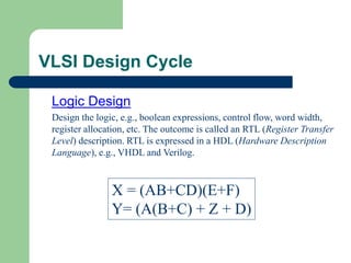
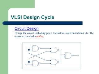
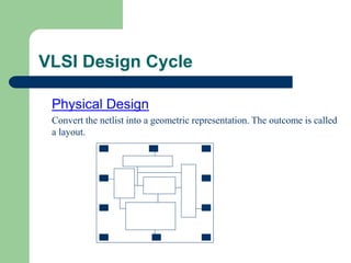
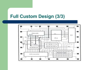
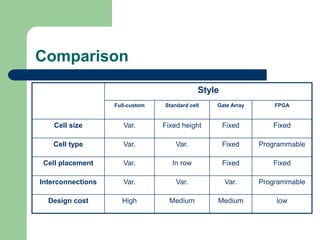
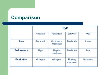
VLSI Design
Introduction
An Overview
 Acronym of VLSI
– Very-Large-Scale Integration
 A VLSI contains more than a million or so
switching devices or logic gates
 Early in the first decade of the 21st century, the
actual number of transistors has exceeded 100
million
Why Make ICs
 Integration improves
– size
– speed
– power
 Integration reduce manufacturing costs
– (almost) no manual assembly
Integrated Circuits Trends
 An entire circuit is manufactured in a single piece of silicon,
first appeared around 1960
 At that time only a few simple gates offering primitive logic
functions such as not, nand, nor etc. could be accommodated
(SSI)
 By 1970 MSI circuits with about a thousand transistors
appeared
 By 1980 LSI circuits of approximately one hundred
thousand devices were possible
IC Evolution
 SSI – Small Scale Integration (early 1970s)
– contained 1 – 10 logic gates
 MSI – Medium Scale Integration
– logic functions, counters
 LSI – Large Scale Integration
– first microprocessors on the chip
 VLSI – Very Large Scale Integration
– now offers 64-bit microprocessors,
complete with cache memory (L1 and often L2),
floating-point arithmetic unit(s), etc.
IC Evolution
 Bipolar technology
– TTL (transistor-transistor logic)
– ECL (emitter-coupled logic)
 MOS (Metal-oxide-silicon)
 Bi-CMOS - hybrid Bipolar, CMOS (for high speed)
 GaAs - Gallium Arsenide (for high speed)
 Si-Ge - Silicon Germanium (for RF)
Choice of Technology
 Two distinct types of technology are fabricated in silicon based upon
– BJT (Bipolar Junction Transistor)
– MOS (Metallic Oxide Semiconductor)
 Since processing of these technologies is very different, it is impractical
to mix them up within a chip.
 MOS logic occupies much smaller area of silicon than the equivalent
BJT logic.
 MOS technology has a much higher potential packing density.
 A MOS logic circuit requires appreciably less current and hence less
power than its bipolar counter part.
 However, bipolar circuits operate faster than MOS circuits
Choice of MOS and BJT
 Even so, the speed-power product for MOS logic compares favorably
with that of BJT logic.
 The structure of an MOS transistor is much simpler than that of bipolar
devices and this makes manufacturing process easier
 This in turn should result in fewer faults occurring in fabrication (high
yield)
 Dynamic logic circuits cannot be implemented in bipolar technology
 Thus in terms of area, power dissipated, yield and flexibility MOS
technology is superior to BJT
Moore’s Law
 Gordon Moore cofounder of Intel Corporation
visualized in the 1970’s that chip building
technology would improve very quickly
 He projected that the number of transistors on a chip
would double about every 18 months
EVIDENCE OF MOORE’S LAW
ACCORDING TO GORDEN MOORE -
(in millions)
1996 MID 1997 1999
YEAR
5 10 20 40
MID 2001
Pentium-I Came In 1996 Transistor Count – 5 Million
Pentium-IV Came In 2001 Transistor Count – 43 Million
Design Methodology
 Top-down design
- Realizing the desired complex behavior of a H/W by
partioing it into an interconnect of simpler subbehavior
- Create lower levels of abstraction from upper levels.
 Bottom-up design
-Aims at realizing the desired complex behavior by suitable
selection and interconnection of parts/components from an
available set of parts/components with known behavior.
- Creates abstractions from low-level behavior.
 Good design needs both top-down and bottom-up efforts.
VLSI Design Flow
VLSI Design Flow
Structured Design Principles
 Hierarchy:
“Divide and conquer” technique involves dividing a module into sub-
modules and then repeating this operation on the sub-modules until the
complexity of the smaller parts becomes manageable.
 Regularity:
The hierarchical decomposition of a large system should result in not
only simple, but also similar blocks, as much as possible.
Regularity usually reduces the number of different modules that need to
be designed and verified, at all levels of abstraction.
Structured Design Principles
 Modularity:
The various functional blocks which make up the larger system must
have well-defined functions and interfaces.
 Locality:
Internal details remain at the local level. The concept of locality also
ensures that connections are mostly between neighboring modules,
avoiding long-distance connections as much as possible.
VLSI design process
Major levels of abstraction:
– specification;
– architecture;
– logic design;
– circuit design;
– layout.
VLSI Design Cycle
VLSI Design Cycle
System Specification
Architectural Design
Logic Design
Circuit Design
Physical Design
Functional Design Fabrication
Packaging
VLSI Design Cycle
System Specification
Specification of the size, speed, power and functionality of the VLSI
system.
Architectural Design
Decisions on the architecture, e.g., RISC/CISC, # of ALU’s, pipeline
structure, cache size, etc. Such decisions can provide an accurate
estimation of the system performance, die size, power consumption, etc.
VLSI Design Cycle
Functional Design
Identify main functional units and their interconnections. No details of
implementation.
VLSI Design Cycle
Logic Design
Design the logic, e.g., boolean expressions, control flow, word width,
register allocation, etc. The outcome is called an RTL (Register Transfer
Level) description. RTL is expressed in a HDL (Hardware Description
Language), e.g., VHDL and Verilog.
X = (AB+CD)(E+F)
Y= (A(B+C) + Z + D)
VLSI Design Cycle
Circuit Design
Design the circuit including gates, transistors, interconnections, etc. The
outcome is called a netlist.
VLSI Design Cycle
Physical Design
Convert the netlist into a geometric representation. The outcome is called
a layout.
VLSI Design Cycle
Fabrication
Process includes lithography, polishing, deposition, diffusion, etc., to
produce a chip.
Packaging
Put together the chips on a PCB (Printed Circuit Board) or an MCM
(Multi-Chip Module)
VLSI Design Cycle
System Specification
Architectural
Specification
RTL in HDL
Netlist
Layout
Timing & relationship
between functional units
Chips
Packaged and
tested chips
Architectural
Design
Functional
Design
Logic
Design
Physical
Design
Fabrication
Packaging
Circuit Design
or
Logic Synthesis
Physical Design Cycle (1/6)
Circuit Partitioning
Floorplanning & Placement
Routing
Layout Compaction
Extraction and Verification
Physical Design Cycle (2/6)
Circuit Partitioning
Partition a large circuit into sub-circuits (called blocks). Factors like
#blocks, block sizes, interconnection between blocks, etc., are
considered.



Physical Design Cycle (3/6)
Floorplanning
Set up a plan for a good layout. Place the modules (modules can be
blocks, functional units, etc.) at an early stage when details like shape,
area, I/O pin positions of the modules, …, are not yet fixed.
Deadspace
Physical Design Cycle (4/6)
Placement – Exact placement of the modules (modules can be
gates, standard cells, etc.) when details of the module design are known.
The goal is to minimize the delay, total area and interconnect cost.
v
Feedthrough
Standard cell type 1
Standard cell type 2
Physical Design Cycle (5/6)
Routing – Complete the interconnections between modules. Factors
like critical path, clock skew, wire spacing, etc., are considered. Include
global routing and detailed routing.
v
Feedthrough
Type 1 standard cel1
Type 2 standard cell
Physical Design Cycle (6/6)
Compaction – Compress the layout from all directions to minimize the
total chip area.
Verification – Check the correctness of the layout. Include DRC (Design
Rule Checking), circuit extraction (generate a circuit from the layout to
compare with the original netlist), performance verification (extract
geometric information to compute resistance, capacitance, delay, etc.)
Design Style(1/3)
Physical design is an extremely complex process , even after breaking
the entire process into several easier steps.
Each step is computationally very hard .
Market requirements demand quick time-to-market and high yield.
As a result, restricted models and design styles are used to reduce the
complexity of physical design.
Design Styles (2/3)
 Broadly DS can be classified as
 Full-Custom ASICs
– Some (possibly all) logic cells are customized and all mask layers are
customized .
 Semicustom ASICs
– All logic cells are predesigned (defined in cell library) and some (possibly
all) of the mask layers are customized
– Types:
Standard-cell based and Gate-array-based ASICs
Design Styles (3/3)
 Programmable ASICs
– All logic cells are predesigned and none of the mask layers are customized
– Types: PLD (Programmable Logic Device) and
FPGA (Field Programmable Gate Array)
Selection of DS depends on factors like
1) type of chip
2) cost
3) time to market, etc.
Full-custom ASICs (1/3)
 Engineers design some or all of the logic cells, circuits, or layout
specifically for one ASIC
– Full-custom ICs are the most expensive to manufacture and to design
– Manufacturing lead time (the time it takes just to make an IC – not
including design time) is typically 8 weeks
Full-custom ASICs (2/3)
 When does it make sense?
– there are no suitable existing cell libraries available
– existing logic cells are not fast enough
– logic cells are not small enough
– logic cells consume too much power
 Trends: fewer and fewer full-custom ICs are being designed (excluding mixed
analog/digital ASICs)
Full Custom Design (3/3)
Standard-Cell-Based ASICs (1/3)
 Cell-Based ASIC (CBIC) uses predesigned cells (AND, OR gates, multiplexers,
flip-flops, ...)
 Standard-cell areas are built of rows of standard cells
 Standard-cell areas can be used in combination with larger predesigned cells
(microcontrollers, or even microprocessors), known as megacells
A cell-based ASIC
(CBIC) die with a
single standard-cell
area combined with 4
fixed blocks
Standard-Cell-Based ASICs(2/2)
 Characteristics
– custom blocks can be embedded;
ASIC designer defines only the placement of the standard cells and the
interconnect in a CBIC
– standard cells can be placed anywhere on a silicon =>
all mask layers of a CBIC are customized
– manufacturing lead time is 8 weeks
Standard-Cell-Based ASICs (3/3)
 Advantages
– designers save time, money, and reduce risks using a predesigned,
pretested, and precharacterized standard-cell library
– standard cells in the library are constructed using full-custom;
each standard cell can be optimized individually
(for example, to maximize speed, minimize area, etc);
 Disadvantages
– time or expense of designing or buying the standard-cell library
– time needed to fabricate all layers of the ASIC for each new design
Gate-Array-Based ASICs
 In gate-array-based ASIC transistors are predefined on the
silicon wafer
– Base cell – the smallest element that is replicated to make
the base array.
– Base array – the predefined pattern of transistors on a
gate array.
 Masked Gate Array (MGA): Only layers which define the
interconnect between transistors are defined by the designer
using custom masks.
Gate-Array-Based ASICs (1/4)
 Since only metal interconnections are unique for MGA,we can use
prefabricated wafers (with completed transistor layers)
– the turnaround time is reduced to a few days or at most a couple of
weeks
– the costs for all the initial prefabrication steps for MGA are shared
for each consumer => the cost of an MGA is reduced compared to
FC and CBIC
 Types: Channeled, Channelless, and Structured Gate Array
Gate-Array-Based ASICs (2/4)
 Channeled gate array
– we leave space between the rows of transistors for wiring
 Characteristics
– only interconnect is customized
– the interconnect uses predefined spaces between rows
– manufacturing lead time is between 2 days and 2 weeks
Gate-Array-Based ASICs (3/4)
 Channelless gate array (sea-of-gates or SOG)
– there are no predefined areas set aside for routing between cells
– we customize the contact layer that defines the connections between
metal1 and transistors
Characteristics
– only some (the top few) mask layers
are customized – the interconnect
– manufacturing lead time is
between 2 days and 2 weeks
Gate-Array-Based ASICs (4/4)
Structured gate array or embedded gate array:
Combines features of CBIC and MGA motivation:
MGA has only fixed gate-array base cell;difficult and inefficient
implementation of memory we set aside some IC area and dedicate it to a
specific function(contain different cells, more suitable for building
memory cells, for example, or complete block, such as a microcontroller)
Characteristics:
- Only some (the top few) mask layers
are customized – the interconnect
- Custom blocks can be embedded
- Manufacturing lead time is
between 2 days and 2 weeks
Problem: embedded function is fixed
Programmable Logic Devices(1/2)
 PLDs
– standard ICs, available in standard configurations
– sold in high volume to many different customers
– PLDs may be configured or programmed to create
a part customized to specific application
 Characteristics
– no customized mask layers or logic cells
– fast design turnaround
– a single large block of programmable interconnect
– a matrix of logic macrocells that usually consists of programmable
array logic followed by a flip-flop or latch
Programmable Logic Devices(2/2)
Types of PLDs
PROM: Uses metal fuse that can be blown permanently
EPROM: Used programmable MOS transistors whose characteristics are altering by
applying a high voltage.
PAL : Programmable Array Logic programmable AND logic array or AND plane,
and fixed OR plane
PLA : Programmable Logic Array programmable AND plane
followed by programmable OR plane
Depending on how the PLD is programmed
erasable PLD (EPLD) mask-programmed PLD
Field-Programmable Gate Arrays
(FPGA)
 FPGA
– a step above the PLD in complexity;
it is usually larger and more complex than a PLD
– rapidly growing in importance
 Characteristics
– none of mask layers are customized
– a method for programming basic cells
and the interconnect
– the core is regular array
of programmable basic logic cells
(combinational + sequential)
– a matrix of programmable interconnect
that surrounds the basic cells
– programmable I/O cells around the core
– design turnaround is a few hours
Comparison
 The choice of design style depends on the intended functionality of
the chip, time to market and total number of chips to be
manufactured.
 Full custom DS is used for microprocessors and other complex
volume applications.
 While FPGA may be used for simple and low volume applications.
 Mixed style may be used.
 For large circuits, it is common to partition the circuit into smaller
subcircuits which are designed using different team.
 Each team may use different DS.
Comparison
Style
Full-custom Standard cell Gate Array FPGA
Cell size Var. Fixed height Fixed Fixed
Cell type Var. Var. Fixed Programmable
Cell placement Var. In row Fixed Fixed
Interconnections Var. Var. Var. Programmable
Design cost High Medium Medium low
Comparison
Style
Full-custom Standard cell Gate Array FPGA
Area Compact Compact to
moderate
Moderate Large
Performance High High to
moderate
Moderate Low
Fabrication All layers All layers Routing
layers only
No layers

VLSI UNIT-1.1.pdf.ppt

  • 1.
  • 2.
    An Overview  Acronymof VLSI – Very-Large-Scale Integration  A VLSI contains more than a million or so switching devices or logic gates  Early in the first decade of the 21st century, the actual number of transistors has exceeded 100 million
  • 3.
    Why Make ICs Integration improves – size – speed – power  Integration reduce manufacturing costs – (almost) no manual assembly
  • 4.
    Integrated Circuits Trends An entire circuit is manufactured in a single piece of silicon, first appeared around 1960  At that time only a few simple gates offering primitive logic functions such as not, nand, nor etc. could be accommodated (SSI)  By 1970 MSI circuits with about a thousand transistors appeared  By 1980 LSI circuits of approximately one hundred thousand devices were possible
  • 5.
    IC Evolution  SSI– Small Scale Integration (early 1970s) – contained 1 – 10 logic gates  MSI – Medium Scale Integration – logic functions, counters  LSI – Large Scale Integration – first microprocessors on the chip  VLSI – Very Large Scale Integration – now offers 64-bit microprocessors, complete with cache memory (L1 and often L2), floating-point arithmetic unit(s), etc.
  • 6.
    IC Evolution  Bipolartechnology – TTL (transistor-transistor logic) – ECL (emitter-coupled logic)  MOS (Metal-oxide-silicon)  Bi-CMOS - hybrid Bipolar, CMOS (for high speed)  GaAs - Gallium Arsenide (for high speed)  Si-Ge - Silicon Germanium (for RF)
  • 7.
    Choice of Technology Two distinct types of technology are fabricated in silicon based upon – BJT (Bipolar Junction Transistor) – MOS (Metallic Oxide Semiconductor)  Since processing of these technologies is very different, it is impractical to mix them up within a chip.  MOS logic occupies much smaller area of silicon than the equivalent BJT logic.  MOS technology has a much higher potential packing density.  A MOS logic circuit requires appreciably less current and hence less power than its bipolar counter part.  However, bipolar circuits operate faster than MOS circuits
  • 8.
    Choice of MOSand BJT  Even so, the speed-power product for MOS logic compares favorably with that of BJT logic.  The structure of an MOS transistor is much simpler than that of bipolar devices and this makes manufacturing process easier  This in turn should result in fewer faults occurring in fabrication (high yield)  Dynamic logic circuits cannot be implemented in bipolar technology  Thus in terms of area, power dissipated, yield and flexibility MOS technology is superior to BJT
  • 9.
    Moore’s Law  GordonMoore cofounder of Intel Corporation visualized in the 1970’s that chip building technology would improve very quickly  He projected that the number of transistors on a chip would double about every 18 months
  • 10.
    EVIDENCE OF MOORE’SLAW ACCORDING TO GORDEN MOORE - (in millions) 1996 MID 1997 1999 YEAR 5 10 20 40 MID 2001 Pentium-I Came In 1996 Transistor Count – 5 Million Pentium-IV Came In 2001 Transistor Count – 43 Million
  • 11.
    Design Methodology  Top-downdesign - Realizing the desired complex behavior of a H/W by partioing it into an interconnect of simpler subbehavior - Create lower levels of abstraction from upper levels.  Bottom-up design -Aims at realizing the desired complex behavior by suitable selection and interconnection of parts/components from an available set of parts/components with known behavior. - Creates abstractions from low-level behavior.  Good design needs both top-down and bottom-up efforts.
  • 12.
  • 13.
  • 14.
    Structured Design Principles Hierarchy: “Divide and conquer” technique involves dividing a module into sub- modules and then repeating this operation on the sub-modules until the complexity of the smaller parts becomes manageable.  Regularity: The hierarchical decomposition of a large system should result in not only simple, but also similar blocks, as much as possible. Regularity usually reduces the number of different modules that need to be designed and verified, at all levels of abstraction.
  • 15.
    Structured Design Principles Modularity: The various functional blocks which make up the larger system must have well-defined functions and interfaces.  Locality: Internal details remain at the local level. The concept of locality also ensures that connections are mostly between neighboring modules, avoiding long-distance connections as much as possible.
  • 16.
    VLSI design process Majorlevels of abstraction: – specification; – architecture; – logic design; – circuit design; – layout.
  • 17.
  • 18.
    VLSI Design Cycle SystemSpecification Architectural Design Logic Design Circuit Design Physical Design Functional Design Fabrication Packaging
  • 19.
    VLSI Design Cycle SystemSpecification Specification of the size, speed, power and functionality of the VLSI system. Architectural Design Decisions on the architecture, e.g., RISC/CISC, # of ALU’s, pipeline structure, cache size, etc. Such decisions can provide an accurate estimation of the system performance, die size, power consumption, etc.
  • 20.
    VLSI Design Cycle FunctionalDesign Identify main functional units and their interconnections. No details of implementation.
  • 21.
    VLSI Design Cycle LogicDesign Design the logic, e.g., boolean expressions, control flow, word width, register allocation, etc. The outcome is called an RTL (Register Transfer Level) description. RTL is expressed in a HDL (Hardware Description Language), e.g., VHDL and Verilog. X = (AB+CD)(E+F) Y= (A(B+C) + Z + D)
  • 22.
    VLSI Design Cycle CircuitDesign Design the circuit including gates, transistors, interconnections, etc. The outcome is called a netlist.
  • 23.
    VLSI Design Cycle PhysicalDesign Convert the netlist into a geometric representation. The outcome is called a layout.
  • 24.
    VLSI Design Cycle Fabrication Processincludes lithography, polishing, deposition, diffusion, etc., to produce a chip. Packaging Put together the chips on a PCB (Printed Circuit Board) or an MCM (Multi-Chip Module)
  • 25.
    VLSI Design Cycle SystemSpecification Architectural Specification RTL in HDL Netlist Layout Timing & relationship between functional units Chips Packaged and tested chips Architectural Design Functional Design Logic Design Physical Design Fabrication Packaging Circuit Design or Logic Synthesis
  • 26.
    Physical Design Cycle(1/6) Circuit Partitioning Floorplanning & Placement Routing Layout Compaction Extraction and Verification
  • 27.
    Physical Design Cycle(2/6) Circuit Partitioning Partition a large circuit into sub-circuits (called blocks). Factors like #blocks, block sizes, interconnection between blocks, etc., are considered.   
  • 28.
    Physical Design Cycle(3/6) Floorplanning Set up a plan for a good layout. Place the modules (modules can be blocks, functional units, etc.) at an early stage when details like shape, area, I/O pin positions of the modules, …, are not yet fixed. Deadspace
  • 29.
    Physical Design Cycle(4/6) Placement – Exact placement of the modules (modules can be gates, standard cells, etc.) when details of the module design are known. The goal is to minimize the delay, total area and interconnect cost. v Feedthrough Standard cell type 1 Standard cell type 2
  • 30.
    Physical Design Cycle(5/6) Routing – Complete the interconnections between modules. Factors like critical path, clock skew, wire spacing, etc., are considered. Include global routing and detailed routing. v Feedthrough Type 1 standard cel1 Type 2 standard cell
  • 31.
    Physical Design Cycle(6/6) Compaction – Compress the layout from all directions to minimize the total chip area. Verification – Check the correctness of the layout. Include DRC (Design Rule Checking), circuit extraction (generate a circuit from the layout to compare with the original netlist), performance verification (extract geometric information to compute resistance, capacitance, delay, etc.)
  • 32.
    Design Style(1/3) Physical designis an extremely complex process , even after breaking the entire process into several easier steps. Each step is computationally very hard . Market requirements demand quick time-to-market and high yield. As a result, restricted models and design styles are used to reduce the complexity of physical design.
  • 33.
    Design Styles (2/3) Broadly DS can be classified as  Full-Custom ASICs – Some (possibly all) logic cells are customized and all mask layers are customized .  Semicustom ASICs – All logic cells are predesigned (defined in cell library) and some (possibly all) of the mask layers are customized – Types: Standard-cell based and Gate-array-based ASICs
  • 34.
    Design Styles (3/3) Programmable ASICs – All logic cells are predesigned and none of the mask layers are customized – Types: PLD (Programmable Logic Device) and FPGA (Field Programmable Gate Array) Selection of DS depends on factors like 1) type of chip 2) cost 3) time to market, etc.
  • 35.
    Full-custom ASICs (1/3) Engineers design some or all of the logic cells, circuits, or layout specifically for one ASIC – Full-custom ICs are the most expensive to manufacture and to design – Manufacturing lead time (the time it takes just to make an IC – not including design time) is typically 8 weeks
  • 36.
    Full-custom ASICs (2/3) When does it make sense? – there are no suitable existing cell libraries available – existing logic cells are not fast enough – logic cells are not small enough – logic cells consume too much power  Trends: fewer and fewer full-custom ICs are being designed (excluding mixed analog/digital ASICs)
  • 37.
  • 38.
    Standard-Cell-Based ASICs (1/3) Cell-Based ASIC (CBIC) uses predesigned cells (AND, OR gates, multiplexers, flip-flops, ...)  Standard-cell areas are built of rows of standard cells  Standard-cell areas can be used in combination with larger predesigned cells (microcontrollers, or even microprocessors), known as megacells A cell-based ASIC (CBIC) die with a single standard-cell area combined with 4 fixed blocks
  • 39.
    Standard-Cell-Based ASICs(2/2)  Characteristics –custom blocks can be embedded; ASIC designer defines only the placement of the standard cells and the interconnect in a CBIC – standard cells can be placed anywhere on a silicon => all mask layers of a CBIC are customized – manufacturing lead time is 8 weeks
  • 40.
    Standard-Cell-Based ASICs (3/3) Advantages – designers save time, money, and reduce risks using a predesigned, pretested, and precharacterized standard-cell library – standard cells in the library are constructed using full-custom; each standard cell can be optimized individually (for example, to maximize speed, minimize area, etc);  Disadvantages – time or expense of designing or buying the standard-cell library – time needed to fabricate all layers of the ASIC for each new design
  • 41.
    Gate-Array-Based ASICs  Ingate-array-based ASIC transistors are predefined on the silicon wafer – Base cell – the smallest element that is replicated to make the base array. – Base array – the predefined pattern of transistors on a gate array.  Masked Gate Array (MGA): Only layers which define the interconnect between transistors are defined by the designer using custom masks.
  • 42.
    Gate-Array-Based ASICs (1/4) Since only metal interconnections are unique for MGA,we can use prefabricated wafers (with completed transistor layers) – the turnaround time is reduced to a few days or at most a couple of weeks – the costs for all the initial prefabrication steps for MGA are shared for each consumer => the cost of an MGA is reduced compared to FC and CBIC  Types: Channeled, Channelless, and Structured Gate Array
  • 43.
    Gate-Array-Based ASICs (2/4) Channeled gate array – we leave space between the rows of transistors for wiring  Characteristics – only interconnect is customized – the interconnect uses predefined spaces between rows – manufacturing lead time is between 2 days and 2 weeks
  • 44.
    Gate-Array-Based ASICs (3/4) Channelless gate array (sea-of-gates or SOG) – there are no predefined areas set aside for routing between cells – we customize the contact layer that defines the connections between metal1 and transistors Characteristics – only some (the top few) mask layers are customized – the interconnect – manufacturing lead time is between 2 days and 2 weeks
  • 45.
    Gate-Array-Based ASICs (4/4) Structuredgate array or embedded gate array: Combines features of CBIC and MGA motivation: MGA has only fixed gate-array base cell;difficult and inefficient implementation of memory we set aside some IC area and dedicate it to a specific function(contain different cells, more suitable for building memory cells, for example, or complete block, such as a microcontroller) Characteristics: - Only some (the top few) mask layers are customized – the interconnect - Custom blocks can be embedded - Manufacturing lead time is between 2 days and 2 weeks Problem: embedded function is fixed
  • 46.
    Programmable Logic Devices(1/2) PLDs – standard ICs, available in standard configurations – sold in high volume to many different customers – PLDs may be configured or programmed to create a part customized to specific application  Characteristics – no customized mask layers or logic cells – fast design turnaround – a single large block of programmable interconnect – a matrix of logic macrocells that usually consists of programmable array logic followed by a flip-flop or latch
  • 47.
    Programmable Logic Devices(2/2) Typesof PLDs PROM: Uses metal fuse that can be blown permanently EPROM: Used programmable MOS transistors whose characteristics are altering by applying a high voltage. PAL : Programmable Array Logic programmable AND logic array or AND plane, and fixed OR plane PLA : Programmable Logic Array programmable AND plane followed by programmable OR plane Depending on how the PLD is programmed erasable PLD (EPLD) mask-programmed PLD
  • 48.
    Field-Programmable Gate Arrays (FPGA) FPGA – a step above the PLD in complexity; it is usually larger and more complex than a PLD – rapidly growing in importance  Characteristics – none of mask layers are customized – a method for programming basic cells and the interconnect – the core is regular array of programmable basic logic cells (combinational + sequential) – a matrix of programmable interconnect that surrounds the basic cells – programmable I/O cells around the core – design turnaround is a few hours
  • 49.
    Comparison  The choiceof design style depends on the intended functionality of the chip, time to market and total number of chips to be manufactured.  Full custom DS is used for microprocessors and other complex volume applications.  While FPGA may be used for simple and low volume applications.  Mixed style may be used.  For large circuits, it is common to partition the circuit into smaller subcircuits which are designed using different team.  Each team may use different DS.
  • 50.
    Comparison Style Full-custom Standard cellGate Array FPGA Cell size Var. Fixed height Fixed Fixed Cell type Var. Var. Fixed Programmable Cell placement Var. In row Fixed Fixed Interconnections Var. Var. Var. Programmable Design cost High Medium Medium low
  • 51.
    Comparison Style Full-custom Standard cellGate Array FPGA Area Compact Compact to moderate Moderate Large Performance High High to moderate Moderate Low Fabrication All layers All layers Routing layers only No layers