Universal asynchronous receiver-transmitter UART Dsa project report
•
0 likes•542 views

A universal asynchronous receiver-transmitter is a computer hardware device for asynchronous serial communication in which the data format and transmission speeds are configurable.

Recommended
More Related Content
What's hot
What's hot (20)
Similar to Universal asynchronous receiver-transmitter UART Dsa project report
Similar to Universal asynchronous receiver-transmitter UART Dsa project report (20)
More from Shahrukh Javed
More from Shahrukh Javed (20)
Recently uploaded
Recently uploaded (20)
Universal asynchronous receiver-transmitter UART Dsa project report
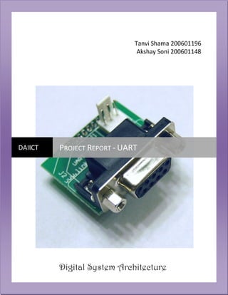
- 1. Tanvi Shama 200601196 Akshay Soni 200601148 DAIICT PROJECT REPORT - UART Digital System Architecture
- 2. 2 Project Report - UART April19,2009 S.No Topic Page No. 1. PROJECT STATEMENT 3 2. FUNCTIONAL SPECIFICATIONS INTRODUCTION 3 BASIC CONCEPT 3 SERIAL CONNECTION 4 APPROACH 4 SYSTEM DIAGRAM 5 FUNCTIONAL BLOCK DIAGRAM 6 3. WORKING TRANSMITTER 7 RECEIVER 8 4. SIMULATIONS 9 5. RTL SCHEMATIC TRANSMITTER 10 RECEIVER 11 6. SYNTHESIS REPORT AND TIMING ANALYSIS 12 7. POST PLACE AND ROUTE SIMULATION 17 8. RUNNING ON ACTUAL HARDWARE BASIC STEPS 18 HYPERTERMINAL SETUP 18 9. VERIFICATION STRATEGY 21 10. REFERENCES 21
- 3. 3 Project Report - UART April19,2009 PROJECT STATEMENT Develop a Verilog based UART (Universal Asynchronous Receiver and Transmitter), and demonstrate its working (as both transmitter and receiver) by interfacing it to Microsoft Windows HyperTerminal. FUNCTIONAL SPECIFICATIONS Introduction UART is a device that has the capability to both receive and transmit serial data. UART exchanges text data in an American Standard Code for Information Interchange (ASCII) format in which each alphabetical character is encoded by 7 bits and transmitted as 8 data bits. For transmission the UART protocol wraps this 8 bit subword with a start bit in the least significant bit (LSB) and a stop bit in the most significant bit (MSB) resulting in a 10 bit word format. Start Data 0 Data 1 Data 2 Data 3 Data 4 Data 5 Data 6 Data 7 Stop Basic Concept UART transmitter controls transmission by fetching a data word in parallel format and directing the UART to transmit it in a serial format. Likewise, the Receiver must detect transmission, receive the data in serial format, strip of the start and stop bits, and store the data word in a parallel format. Since the UART is asynchronous in working, the receiver does not know when the data will come, so receiver generate local clock in order to synchronize to transmitter whenever start bit is received. Asynchronous transmission allows data to be transmitted without the sender having to send a clock signal to the receiver. The transmitter and receiver agree on timing parameters in advance and special bits are added to each word which is used to synchronize the sending and receiving units. When a word is given to the UART for Asynchronous transmission, a bit called the “Start Bit” is added to the beginning of each word that is to be transmitted. The Star Bit is used to alert the receiver that a word of data is about to be sent, and to force the clock in the receiver into synchronization with the clock in the transmitter. After the Start Bit, the individual bits of the word of data are sent, with the Least Significant Bit (LSB) being sent first. Each bit in the transmission is transmitted for exactly the same amount of time as all of the other bits, and the receiver “looks” at the wire at approximately halfway through the period assigned to each bit to determine if the bit is a 1 or a 0. For example, if it takes two seconds to send each bit, the receiver will examine the signal to determine if it is a 1 or a 0 after one second has passed, then it will wait two seconds and then examine the value of the next bit, and so on. Then at least one
- 4. 4 Project Report - UART April19,2009 Stop Bit is sent by the transmitter. Because asynchronous data is “self synchronous”, if there is no data to transmit, the transmission line can be idle. Serial Connection Serial Port used for UART is RS-232. It is a nine pin connector with each pin assigned with different functionality. Approach We approached the given problem statement by implementing the UART receiver and transmitter independently. First we tried to implement the UART transmitter due to its less complexity in working and implementation. We used 9600 BAUD rate for transmission of serial data and divided the system clock accordingly. Then we started to implement the UART receiver. We learned the concept of clock synchronization by taking the clock many times higher that the transmitting rate. For this we generated clock which is 8 times the transmitter BAUD rate to minimize the distortions in the incoming data. We followed the Finite State Machine (FSM) approach to code both UART transmitter and receiver.
- 5. 5 Project Report - UART April19,2009 System Diagram HyperTerminal (Transmitted Data) Spartan 3E 8 – LEDs 4–PushButton 4-Switches RS- 232 Single Bit Transmission Single Bit Transmission 8 Bits 8Bits Select Load Shift Received Data Reset The above figure shows the overall working of the UART and the HyperTerminal. UART as transmitter takes 8 – bit data from the switches and then transmits it bitwise through the RS-232 port and is displayed on the HyperTerminal of target machine. The “load switch” is used to load the transmit register of the UART and the “shift switch” is used to shift the data out from the shift register of the UART. UART as a receiver accepts the 8 – bit data word from the HyperTerminal through the RS-232 port and displays it on the LED’s. The clock used by the UART receiver is 8 times the clock of the transmitter.
- 6. 6 Project Report - UART April19,2009 Functional Block Diagram o Transmitter Where [7:0] din 8 bit data to be transmitted. Load loads the transmit register with the data. Shift shifts the data out from the shift register. [1:0] select for selecting din. [3:0] CS FSM state output. Ready indicates when ready to receive data to transmit. o Receiver [7:0] din load shift [1:0] select reset clk1 UART Transmitter Datapath Controller [3:0] CS ready UART Receiver Datapath Controller read_not_ready_out shift load Error1 Error2 clr_Sample_counter inc_Sample_counter clr_Bit_counter inc_Bit_counter read_not_ready_in Serial_in Sample_counter Bit_counter Sample_clk1 enable
- 7. 7 Project Report - UART April19,2009 Where read_not_ready_in signals that the host is not ready to receive data. Serial_in serial bit stream received by the unit. enable active enable bit. Sample_counter counts the samples of a bit. Bit_counter counts the bits that have been sampled. read_not_ready_out signals that the receiver has received 8 bits. inc_sample_counter increments Sample_counter. clr_Sample_counter clears Sample_counter. inc_Bit_counter increments Bit_counter. clr_Bit_counter clears Bit_counter. load causes RCV_shftreg to transfer data to RCV_datareg. shift causes RCV_shftreg to shift towards the LSB. Error1 asserts if host is not ready to receive data. Error2 asserts if the stop bit is missing. WORKING Transmitter UART_idle UART_stopbit UART_bit0 UART_bit1 UART_bit2 UART_bit3 UART_bit5 UART_startbit UART_bit7 UART_bit6 UART_bit4 readyandshift shift shift shift shift shift shift shift shift shift !readyandshift else else else else else else else else else else else reset UARTTransmitterFSM
- 8. 8 Project Report - UART April19,2009 Receiver idle Serial_in = 0 starting Serial_in = 1 Sample_count er =3 Clr_Sample_counter Receiving / inc_Sample_counter Sample_count er = 7 Bit_counter = 8 Read_not_ready_out Clr_Sample_counter Clr_Bit_counter Read_not_rea dy_in Inc_Sample_counter Shift Inc_Bit_counter Clr_Sample_counter Error1 Serial_in = 0 Error2 load clr_Sample_counter enable 1 1 1 1 1 1 1
- 9. 9 Project Report - UART April19,2009 SIMULATIONS Transmitter Receiver We didn’t see the simulation results for the UART receiver and implemented the design directly on chip which produced the desired results.
- 10. 10 Project Report - UART April19,2009 RTL SCHEMATIC Transmitter
- 11. 11 Project Report - UART April19,2009 Receiver
- 12. 12 Project Report - UART April19,2009 SYNTHESIS REPORT AND TIMING ANALYSIS Transmitter o Synthesis Report ========================================================================= HDL Synthesis Report Macro Statistics # ROMs : 1 4x8-bit ROM : 1 # Counters : 1 32-bit up counter : 1 # Registers : 6 1-bit register : 3 4-bit register : 1 8-bit register : 1 9-bit register : 1 ========================================================================= ========================================================================= * Final Report * ========================================================================= Final Results RTL Top Level Output File Name : uarttx.ngr Top Level Output File Name : uarttx Output Format : NGC Optimization Goal : Speed Keep Hierarchy : NO Design Statistics # IOs : 12 Cell Usage : # BELS : 141 # GND : 1 # INV : 4 # LUT1 : 31 # LUT2 : 5 # LUT3 : 7 # LUT3_D : 1 # LUT4 : 17 # LUT4_D : 1 # MUXCY : 39 # MUXF5 : 3 # VCC : 1 # XORCY : 31 # FlipFlops/Latches : 52 # FDC : 4 # FDCE : 1
- 13. 13 Project Report - UART April19,2009 # FDE : 6 # FDPE : 9 # FDR : 32 # Clock Buffers : 1 # BUFGP : 1 # IO Buffers : 11 # IBUF : 5 # OBUF : 6 ========================================================================= Device utilization summary: --------------------------- Selected Device : 3s500efg320-5 Number of Slices: 35 out of 4656 0% Number of Slice Flip Flops: 52 out of 9312 0% Number of 4 input LUTs: 66 out of 9312 0% Number of IOs: 12 Number of bonded IOBs: 12 out of 232 5% Number of GCLKs: 1 out of 24 4% ========================================================================== o Timing Report ============================================================================== Clock Information: -----------------------------------+------------------------+-------+ Clock Signal | Clock buffer(FF name) | Load | -----------------------------------+------------------------+-------+ clk1 | BUFGP | 33 | clock | NONE(Hold_2) | 19 | -----------------------------------+------------------------+-------+ INFO:Xst:2169 - HDL ADVISOR - Some clock signals were not automatically buffered by XST with BUFG/BUFR resources. Please use the buffer_type constraint in order to insert these buffers to the clock signals to help prevent skew problems. Asynchronous Control Signals Information: ---------------------------------------- -----------------------------------+------------------------+-------+ Control Signal | Buffer(FF name) | Load | -----------------------------------+------------------------+-------+ reset | IBUF | 14 | -----------------------------------+------------------------+-------+
- 14. 14 Project Report - UART April19,2009 Timing Summary: --------------- Speed Grade: -5 Minimum period: 6.207ns (Maximum Frequency: 161.095MHz) Minimum input arrival time before clock: 6.804ns Maximum output required time after clock: 4.655ns Maximum combinational path delay: No path found ========================================================================= Timing constraint: Default period analysis for Clock 'clock' Clock period: 6.207ns (frequency: 161.095MHz) Total number of paths / destination ports: 173 / 24 ------------------------------------------------------------------------- Delay: 6.207ns (Levels of Logic = 3) Source: CS_0 (FF) Destination: ready (FF) Source Clock: clock rising Destination Clock: clock rising Receiver o Synthesis Report ========================================================================= HDL Synthesis Report Macro Statistics # Counters : 3 32-bit up counter : 1 4-bit up counter : 1 5-bit up counter : 1 # Registers : 3 1-bit register : 1 8-bit register : 2 # Comparators : 1 4-bit comparator less : 1 ========================================================================= ========================================================================= * Final Report * ========================================================================= Final Results RTL Top Level Output File Name : UART_RX.ngr Top Level Output File Name : UART_RX Output Format : NGC Optimization Goal : Speed Keep Hierarchy : NO Design Statistics
- 15. 15 Project Report - UART April19,2009 # IOs : 15 Cell Usage : # BELS : 143 # GND : 1 # INV : 5 # LUT1 : 31 # LUT2 : 3 # LUT2_L : 1 # LUT3 : 7 # LUT3_L : 1 # LUT4 : 19 # LUT4_D : 2 # MUXCY : 39 # MUXF5 : 2 # VCC : 1 # XORCY : 31 # FlipFlops/Latches : 60 # FDE : 1 # FDR : 33 # FDRE : 25 # FDRS : 1 # Clock Buffers : 2 # BUFG : 1 # BUFGP : 1 # IO Buffers : 14 # IBUF : 3 # OBUF : 11 ========================================================================= Device utilization summary: --------------------------- Selected Device : 3s500efg320-5 Number of Slices: 42 out of 4656 0% Number of Slice Flip Flops: 60 out of 9312 0% Number of 4 input LUTs: 69 out of 9312 0% Number of IOs: 15 Number of bonded IOBs: 15 out of 232 6% Number of GCLKs: 2 out of 24 8% =========================================================================
- 16. 16 Project Report - UART April19,2009 o Timing Report ========================================================================= Clock Information: ------------------ -----------------------------------+------------------------+-------+ Clock Signal | Clock buffer(FF name) | Load | -----------------------------------+------------------------+-------+ Sample_clk1 | BUFGP | 33 | Sample_clk2 | BUFG | 27 | -----------------------------------+------------------------+-------+ Asynchronous Control Signals Information: ---------------------------------------- No asynchronous control signals found in this design Timing Summary: --------------- Speed Grade: -5 Minimum period: 5.790ns (Maximum Frequency: 172.701MHz) Minimum input arrival time before clock: 5.624ns Maximum output required time after clock: 9.315ns Maximum combinational path delay: 6.543ns ========================================================================= Timing constraint: Default period analysis for Clock 'Sample_clk2' Clock period: 5.790ns (frequency: 172.701MHz) Total number of paths / destination ports: 405 / 61 ------------------------------------------------------------------------- Delay: 5.790ns (Levels of Logic = 3) Source: Sample_counter_3 (FF) Destination: Sample_counter_0 (FF) Source Clock: Sample_clk2 rising Destination Clock: Sample_clk2 rising
- 17. 17 Project Report - UART April19,2009 POST PLACE AND ROUTE SIMULATION Floor plan
- 18. 18 Project Report - UART April19,2009 RUNNING ON ACTUAL HARDWARE Basic Steps In Xilinx click on Generate Programming File and then when it is complete click on Configure device (iMPACT). Then program the chip using this utility and on successful completion we will get an alert. Now we are ready to use it on hardware. We then have to configure the HyperTerminal as explained in next section. Now for receiver code if we type something on HyperTerminal, the value will be reflected on LEDs and in transmitter anything given from switches will be displayed on HyperTerminal. For transmitter first we select from two switches what we want to send. Then we reset, followed by load followed by shift. The character chosen will be then displayed on HyperTerminal. For receiver first we need to put on the enable switch and then anything typed on HyperTerminal will be displayed on LEDs. HyperTerminal Setup Figure 1: New Connection Screen
- 19. 19 Project Report - UART April19,2009 Figure 2: Connect To Screen Figure 3: Settings
- 20. 20 Project Report - UART April19,2009 Figure 4: Transmitter Settings Figure 5: Receiver Settings
- 21. 21 Project Report - UART April19,2009 VERIFICATION STRATEGY For verification we followed the White Box Testing approach. While doing testing, we took into consideration following points: Is the data being sent from HyperTerminal is displayed properly on LEDs. Are we able to see the desired data on HyperTerminal when we send something from FPGA? Is the sample clock (8 times transmission clock) generated properly? We did simulations for both transmitter and receiver (not giving the simulation but working fine with hardware) on Xilinx ISE and the results are displayed in the Simulation section above. We calculated the Hexadecimal values of all the characters by hand and then matched the results of the kit with the calculations done by hand. For black box testing we gave different inputs and observed the outputs and matched them with desired ones which are beforehand known. If the sample clock generated at the receiver is not 8 times the transmitter clock then the output will differ from those of the correct ones. REFERENCES Advance Digital Design using Verilog HDL by Michael D Ciletti. http://bwrc.eecs.berkeley.edu/people/grad_students/tinas/Fall04SFSU852/Lectures/UARTTrans mitterdoneinclassRev1.doc http://www.lammertbies.nl/comm/info/serial-uart.html http://www.linksprite.com/images/UART-RS232-1.jpg http://www.cyq.com/htdocs/hyperterminal.htm
- 22. 22 Project Report - UART April19,2009 ANNEXURE A Transmitter //------------------------------------------------------------------------ --------- // Uart Transmit Module // // Author: Akshay Soni (200601148) // Tanvi Sharma (200601196) // // parameters: // din.........8 bit bus of data that is to be sent out // load........This signal write the data to a holding register and sets a Ready flag to let the // transmitter know that there is data ready to go out. // clk1........system clock. // reset.......system reset, returns uart to an idle state and clears ready. // shift.......signal to let the system know when it is time to shift a bit(this is the baud rate). // txd.........transmit data output. // ready.......status: 0 indicates no data in holding register. // status: 1 indicates holding register is full. //------------------------------------------------------------------------ -------------------------- module uarttx(load,clk1,reset,shift,txd,ready,CS,select); input load; // loads the transmit register input clk1; // 1x transmit clock input reset; // resets the registers input [1:0] select; // to select the data to be transmitted input shift; // this is when the shift register is supposed to shift output txd; // output data output ready; // indicates ready to recieve char to transmit output [3:0]CS; // states of the output reg ready; // ready status bit reg txd; // transmit bit reg [8:0] INT; // nine bit shift register reg [7:0] Hold; // holding register for the data reg doshift; // tells the shift register to shift its data reg doload; // tells the shift register to load its data reg clearready; // tells the ready bit to clear reg setready; // tells the ready bit to set reg clock = 1'b0; reg [7:0] din = 8'h61; // data to be transmitted integer a = 0; // integer used for clock division
- 23. 23 Project Report - UART April19,2009 always @(select) begin case(select) 2'b00: din = 8'h62; 2'b01: din = 8'h63; 2'b10: din = 8'h64; 2'b11: din = 8'h65; default: din = 8'h61; endcase end always @(posedge clk1) begin if(a == 2604) begin a = 0; clock = ~clock; end else a = a+1; end always @(posedge clock) begin if(load) begin Hold <= din; //load data into holding register end end always @(load) if(load) setready <= 1; else setready <= 0; //------------------------------------------------------------------------ // Uart State machine // // LSB is the first bit to be transmitted in UART transmission. // But the naming of the states is different from that. // //------------------------------------------------------------------------ - parameter [3:0] UART_IDLE = 4'b0000, UART_STARTBIT = 4'b0001, UART_BIT7 = 4'b0010, UART_BIT6 = 4'b0011,
- 24. 24 Project Report - UART April19,2009 UART_BIT5 = 4'b0100, UART_BIT4 = 4'b0101, UART_BIT3 = 4'b0110, UART_BIT2 = 4'b0111, UART_BIT1 = 4'b1000, UART_BIT0 = 4'b1001, UART_STOPBIT = 4'b1010; // Declaration of current state and next state variables reg [3:0] CS; reg [3:0] NS; always @ (posedge clock or posedge reset) begin if (reset) CS <= UART_IDLE; else CS <= NS; end always @ (CS or ready or shift) begin case (CS) // case statement for the states UART_IDLE: begin if (ready && shift) begin NS <= UART_STARTBIT; doshift = 0; doload = 1; //load data into shift register clearready = 1; //clear ready bit end else begin NS <= UART_IDLE; doshift = 0; doload = 0; clearready = 0; end end UART_STARTBIT: begin if(shift) begin NS <= UART_BIT7; //go to next state doshift = 1; //shift data out register doload = 0; clearready = 0; end else begin NS <= UART_STARTBIT; //hold this state doshift = 0; doload = 0; clearready = 0; end end UART_BIT7: begin if(shift) begin NS <= UART_BIT6; //go to next state
- 25. 25 Project Report - UART April19,2009 doshift = 1; //shift data out register doload = 0; clearready = 0; end else begin NS <= UART_BIT7; //hold this state doshift = 0; doload = 0; clearready = 0; end end UART_BIT6: begin if(shift) begin NS <= UART_BIT5; //go to next state doshift = 1; //shift data out register doload = 0; clearready = 0; end else begin NS <= UART_BIT6; //hold this state doshift = 0; doload = 0; clearready = 0; end end UART_BIT5: begin if(shift) begin NS <= UART_BIT4; //go to next state doshift = 1; //shift data out register doload = 0; clearready = 0; end else begin NS <= UART_BIT5; //hold this state doshift = 0; doload = 0; clearready = 0; end end UART_BIT4: begin if(shift) begin NS <= UART_BIT3; //go to next state doshift = 1; //shift data out register doload = 0; clearready = 0; end else begin NS <= UART_BIT4; //hold this state doshift = 0; doload = 0; clearready = 0; end end
- 26. 26 Project Report - UART April19,2009 UART_BIT3: begin if(shift) begin NS <= UART_BIT2; //go to next state doshift = 1; //shift data out register doload = 0; clearready = 0; end else begin NS <= UART_BIT3; //hold this state doshift = 0; doload = 0; clearready = 0; end end UART_BIT2: begin if(shift) begin NS <= UART_BIT1; //go to next state doshift = 1; //shift data out register doload = 0; clearready = 0; end else begin NS <= UART_BIT2; //hold this state doshift = 0; doload = 0; clearready = 0; end end UART_BIT1: begin if(shift) begin NS <= UART_BIT0; //go to next state doshift = 1; //shift data out register doload = 0; clearready = 0; end else begin NS <= UART_BIT1; //hold this state doshift = 0; doload = 0; clearready = 0; end end UART_BIT0: begin if(shift) begin NS <= UART_STOPBIT; //go to next state doshift = 1; //shift data out register doload = 0; clearready = 0; end else begin NS <= UART_BIT0; //hold this state doshift = 0; doload = 0; clearready = 0;
- 27. 27 Project Report - UART April19,2009 end end UART_STOPBIT: begin if(shift && !ready) begin NS <= UART_IDLE; //nothing more to do, so idle doshift = 0; doload = 0; clearready = 0; end else if (shift && ready) begin NS <= UART_STARTBIT; //another byte waiting, go do it doshift = 0; doload = 1; //load data into shift register clearready = 1; //clear ready bit end else begin NS <= UART_STOPBIT; //hold this state doshift = 0; doload = 0; clearready = 0; end end default: begin doshift = 0; doload = 0; clearready = 0; NS <= UART_IDLE; end endcase end //--------------------------------------------------------------- // shift register // // shift register can do a load, and do a shift //--------------------------------------------------------------- always @(posedge clock or posedge reset) begin if(reset) begin INT <= 9'b111111111; //reset transmit register to all 1's end else begin if(doload) begin INT <= {Hold,1'b0}; //load data and set start bit to 0 txd <= INT[0]; end else if (doshift) begin INT <= {1'b1,INT[8:1]}; //shift data, shift in 1's txd <= INT[0]; end else begin
- 28. 28 Project Report - UART April19,2009 INT <= INT; //hold data txd <= INT[0]; end end end //--------------------------------------------------------------- // ready status bit // when status == 1, this indicates that there is data waiting // in the data holding register ready to be // transmitted. // when status == 0, data holding register is empty //--------------------------------------------------------------- always @ (posedge clock or posedge reset) begin if(reset) ready <= 0; //always not ready at reset else begin if(setready) ready <= 1; else if(clearready) ready <= 0; else ready <= ready; //hold ready end end endmodule
- 29. 29 Project Report - UART April19,2009 Receiver `timescale 1ns / 1ps ///////////////////////////////////////////////////////////////////////////// ///// // Uart Transmit Module // // Author: Akshay Soni (200601148) // Tanvi Sharma (200601196) // // // // // // // ///////////////////////////////////////////////////////////////////////////// ///// module UART_RX(RCV_datareg,read_not_ready_out,Error1,Error2,Serial_in,read_not_ready _in,Sample_clk1, enable); parameter word_size = 8; parameter half_word = word_size/2; parameter Num_counter_bits = 4; parameter Num_state_bits = 2; parameter idle = 2'b00; parameter starting = 2'b01; parameter receiving = 2'b10; output [word_size-1:0] RCV_datareg; output read_not_ready_out, Error1, Error2; input Serial_in, Sample_clk1, enable, read_not_ready_in; reg Sample_clk = 1'b0; reg RCV_datareg; reg [word_size-1:0] RCV_shftreg; reg [Num_counter_bits-1:0] Sample_counter; reg [Num_counter_bits:0] Bit_counter; reg [Num_state_bits-1:0] state,next_state; reg inc_Bit_counter, clr_Bit_counter; reg inc_Sample_counter,clr_Sample_counter; reg shift, load, read_not_ready_out; reg Error1, Error2; integer a = 0;
- 30. 30 Project Report - UART April19,2009 always @(posedge Sample_clk1) begin if(a == 326) begin Sample_clk <= ~Sample_clk; a <= 0; end else a <= a+1; end always @ (state or Serial_in or read_not_ready_in or Sample_counter or Bit_counter) begin read_not_ready_out = 0; clr_Sample_counter = 0; clr_Bit_counter = 0; inc_Sample_counter = 0; inc_Bit_counter = 0; shift = 0; Error1 = 0; Error2 = 0; load = 0; next_state = state; case(state) idle: if(Serial_in == 0)begin next_state = starting; end starting: if(Serial_in == 1)begin next_state = idle; clr_Sample_counter = 1; end else if(Sample_counter == half_word-1)begin next_state = receiving; clr_Sample_counter = 1; end else inc_Sample_counter = 1; receiving: if(Sample_counter < word_size-1) begin inc_Sample_counter = 1; next_state = receiving; end else begin clr_Sample_counter = 1; if(Bit_counter != word_size)begin shift = 1; inc_Bit_counter = 1; end else begin next_state = idle;
- 31. 31 Project Report - UART April19,2009 read_not_ready_out = 1; clr_Bit_counter = 1; if(read_not_ready_in == 1)Error1 = 1; else if(Serial_in == 0)Error2 = 1; else load = 1; end end default: next_state = idle; endcase end always @ (posedge Sample_clk) begin if(enable == 0)begin state <= idle; Sample_counter <= 0; Bit_counter <= 0; RCV_datareg <= 0; RCV_shftreg <= 0; end else begin state <= next_state; if(clr_Sample_counter == 1)Sample_counter<=0; else if(inc_Sample_counter == 1)Sample_counter <= Sample_counter + 1; if(clr_Bit_counter == 1)Bit_counter <= 0; else if(inc_Bit_counter == 1)Bit_counter <= Bit_counter + 1; if(shift == 1)RCV_shftreg <= {Serial_in, RCV_shftreg[word_size-1:1]}; if(load == 1)RCV_datareg <= RCV_shftreg; end end endmodule