Downloaded 167 times

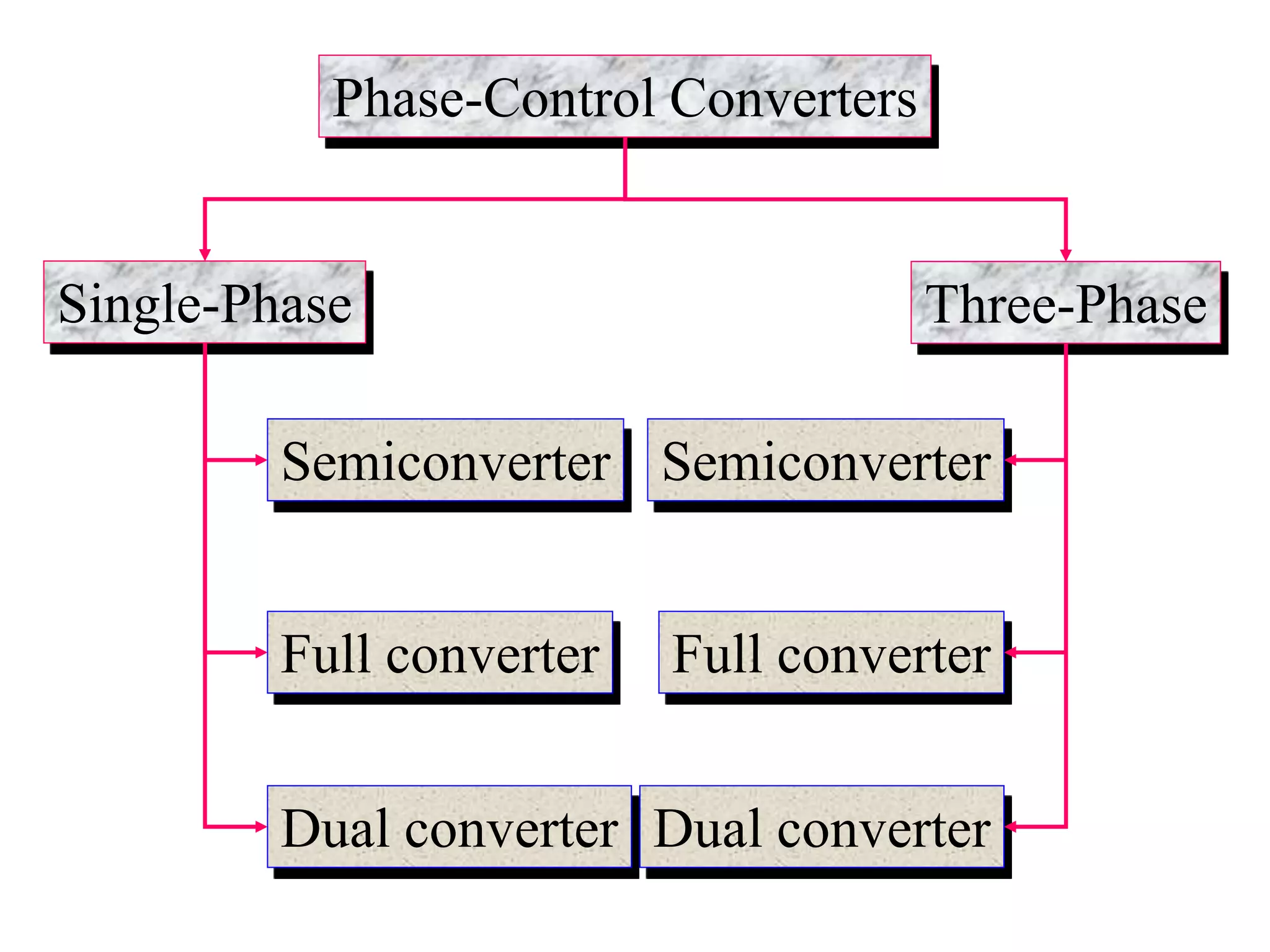
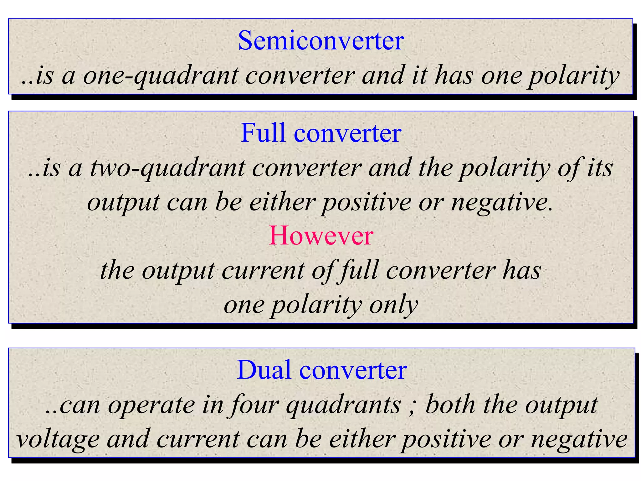


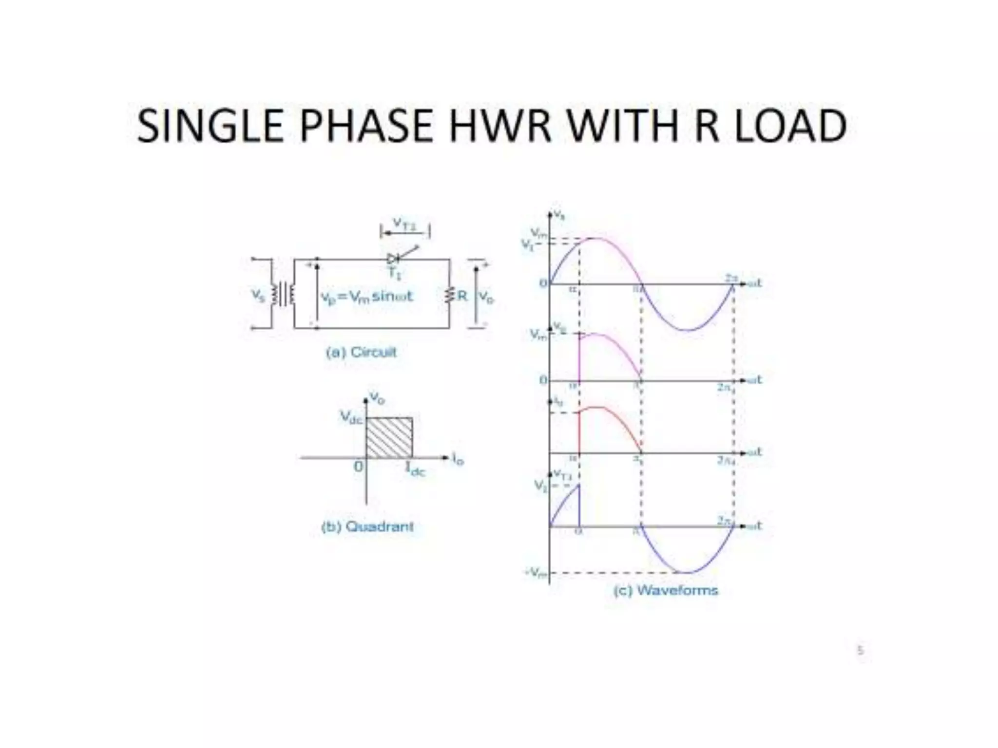


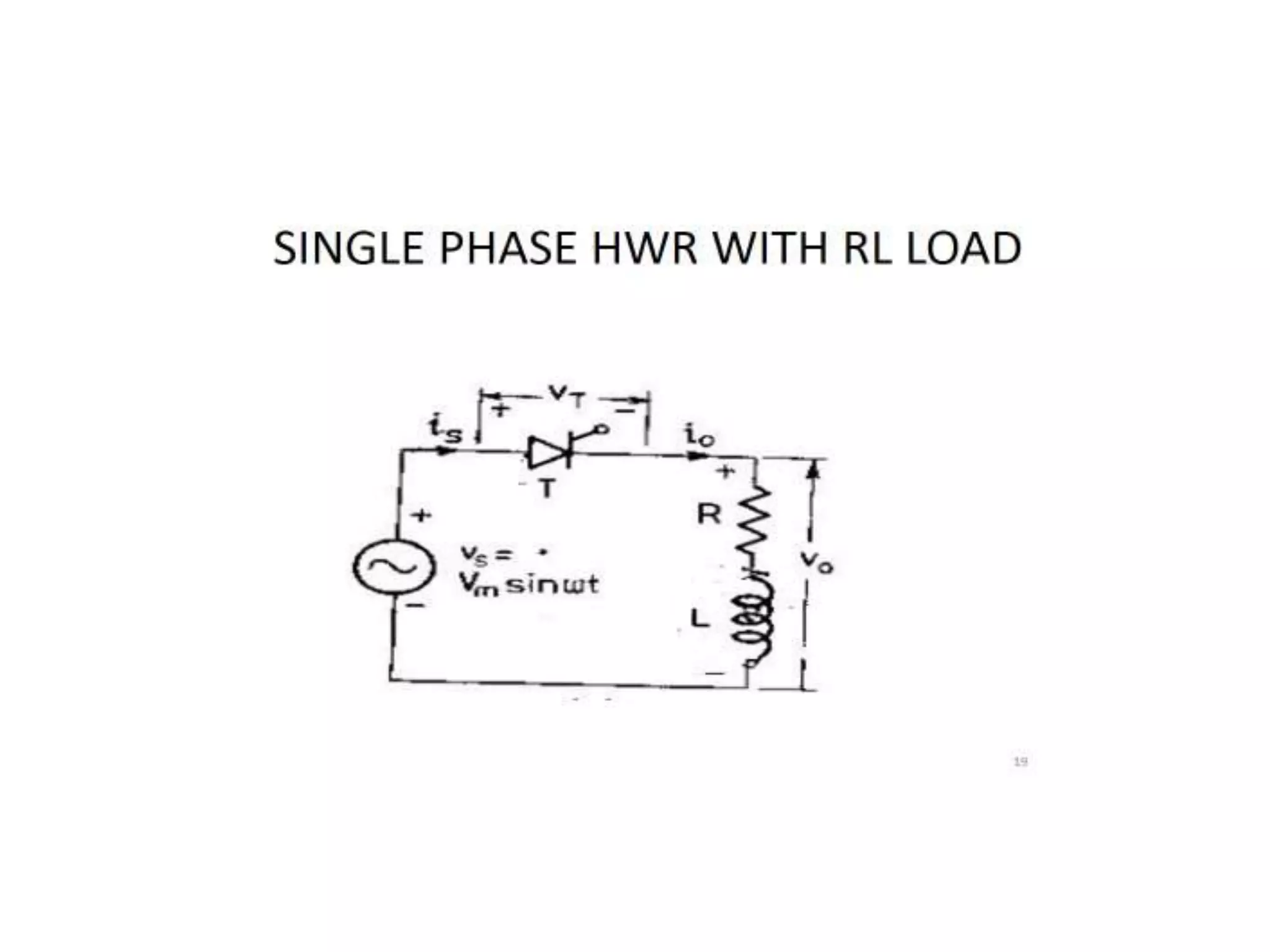


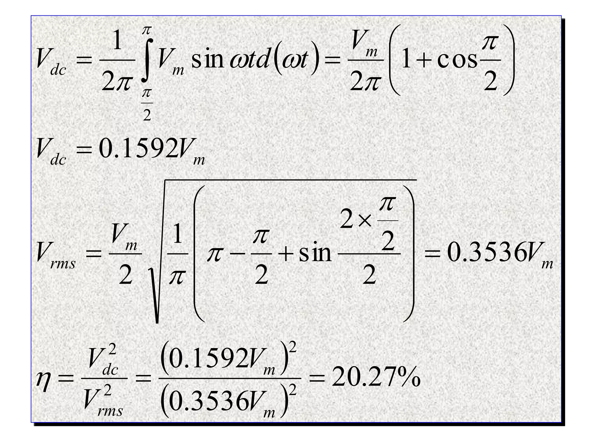


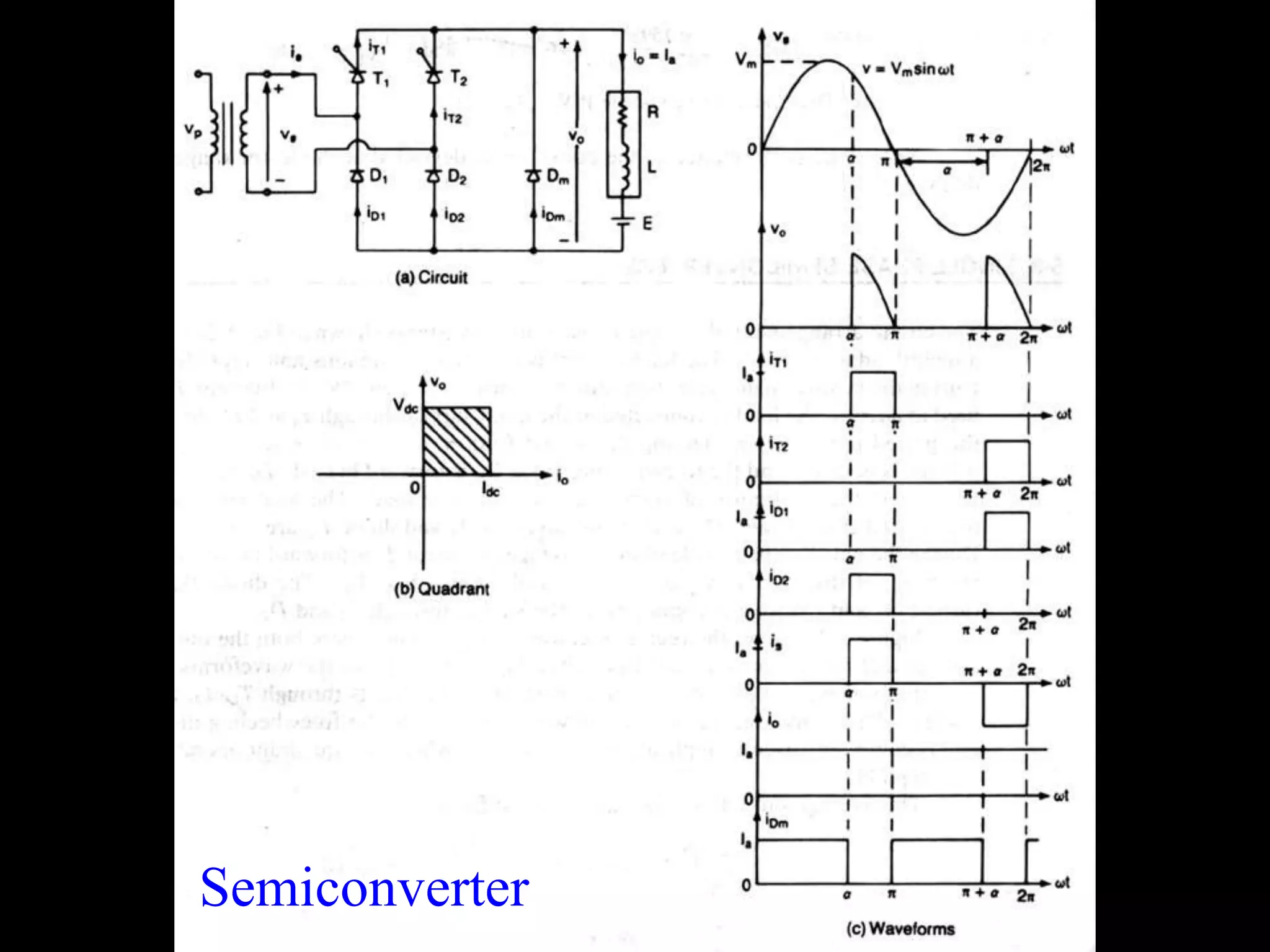
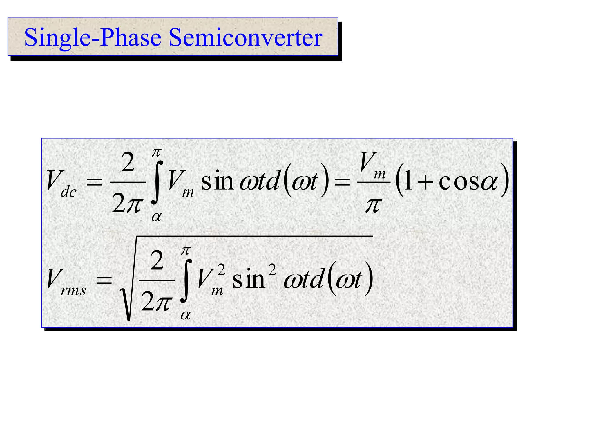


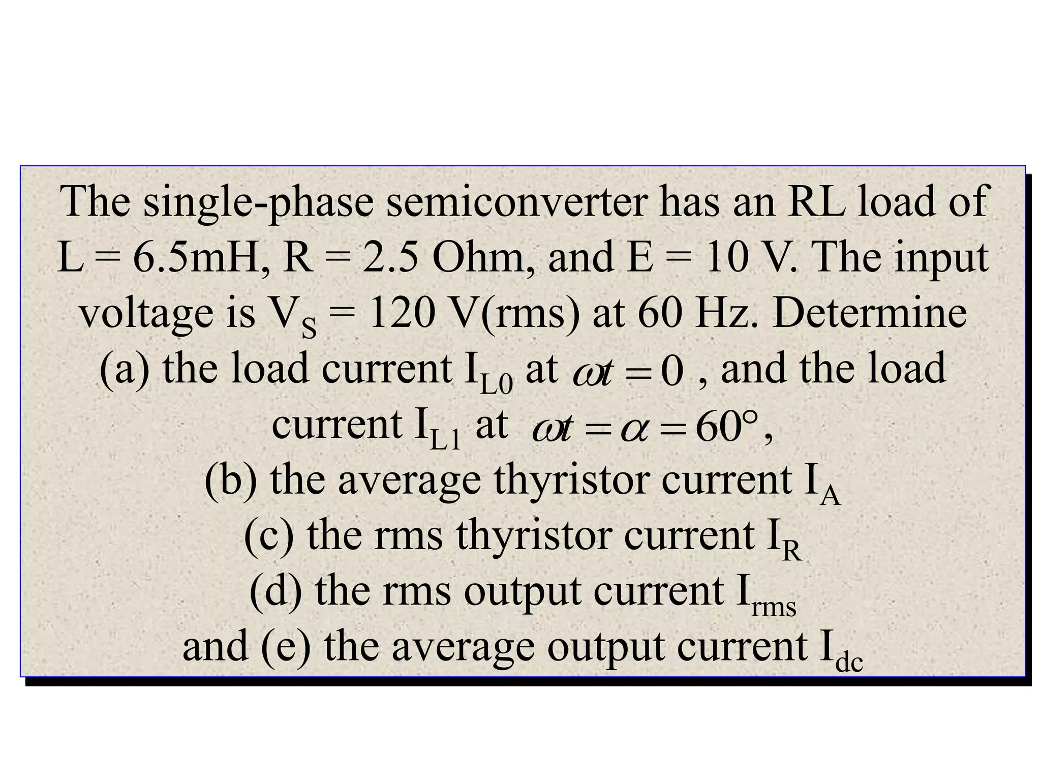
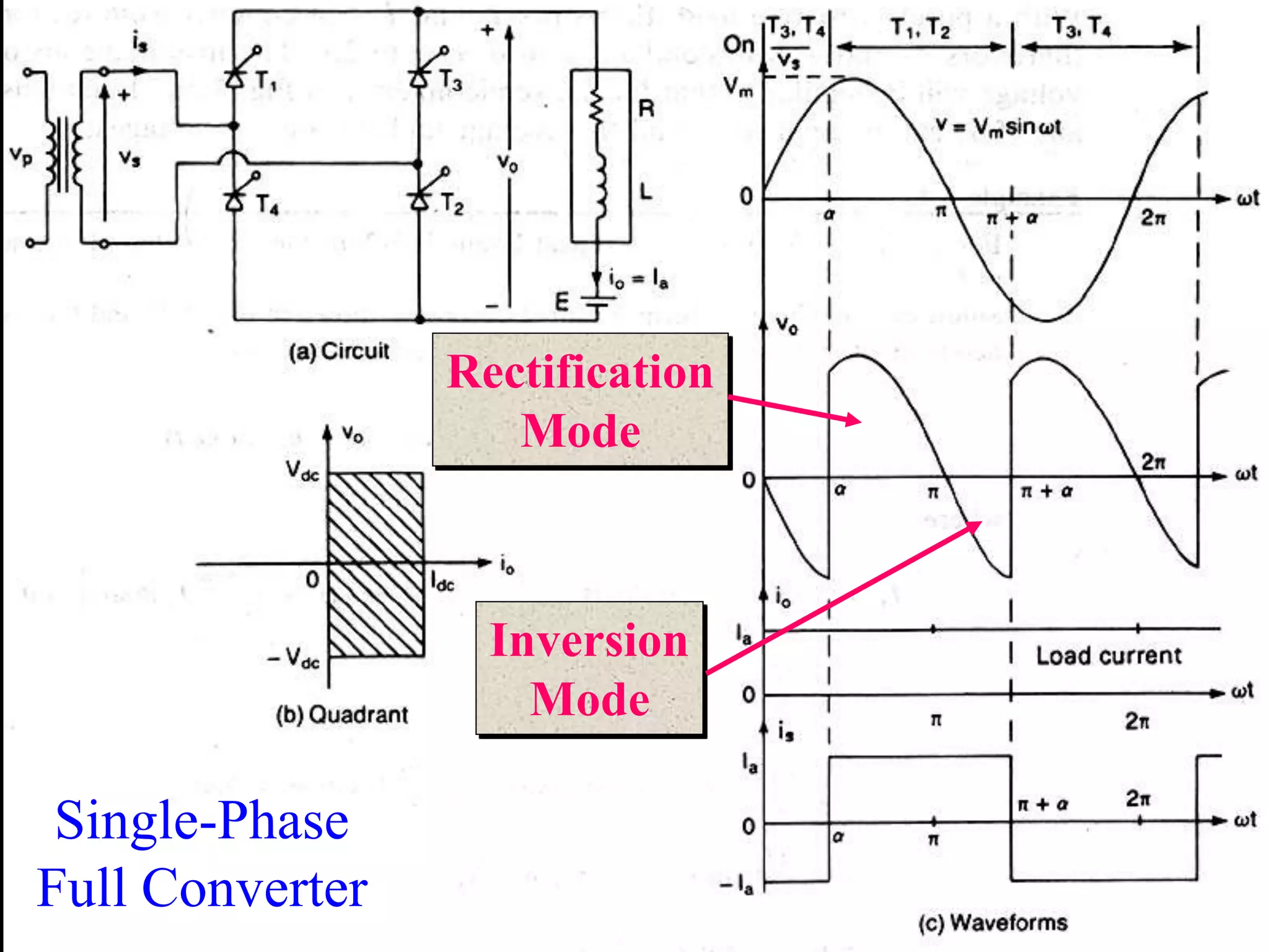
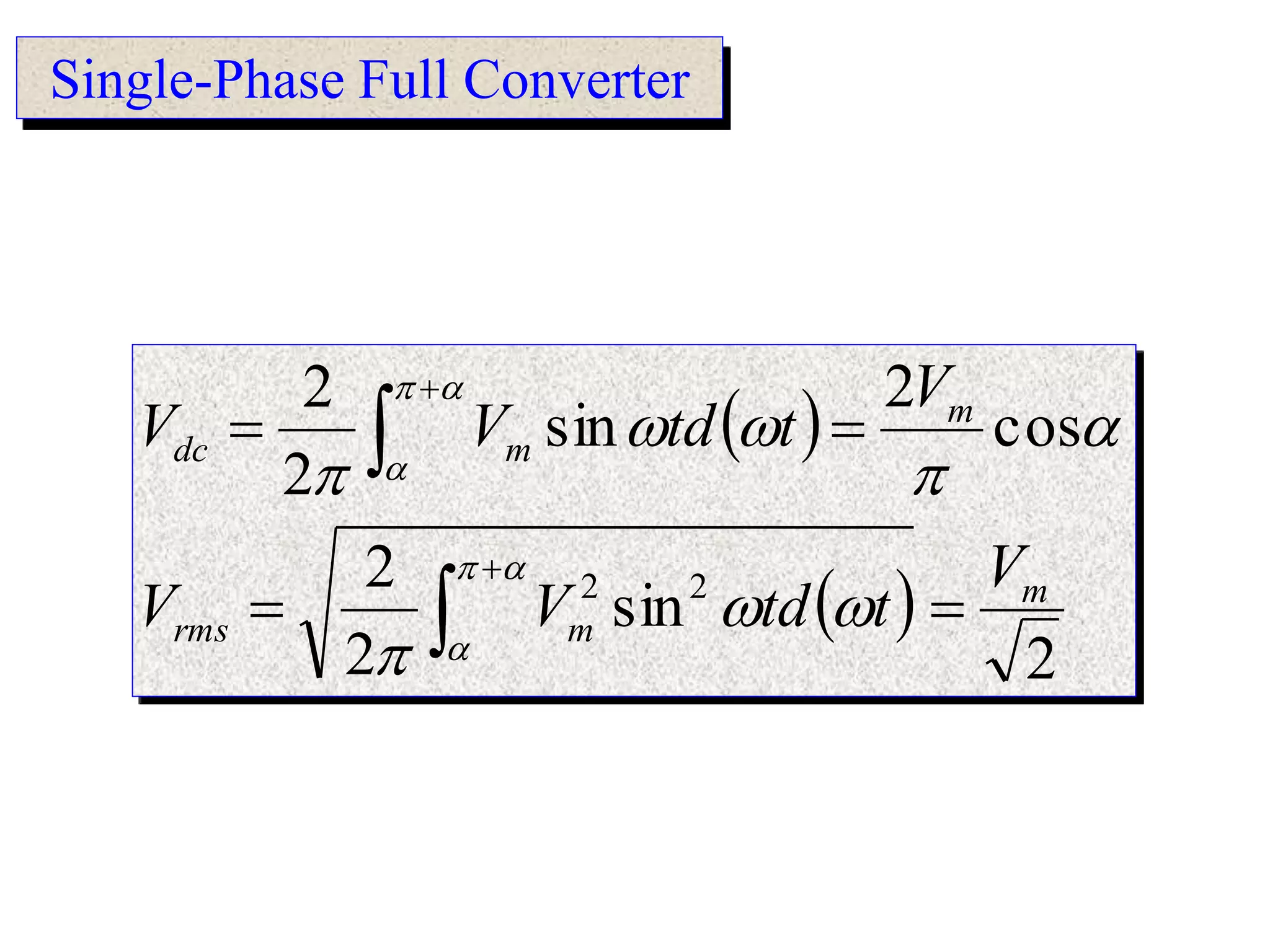


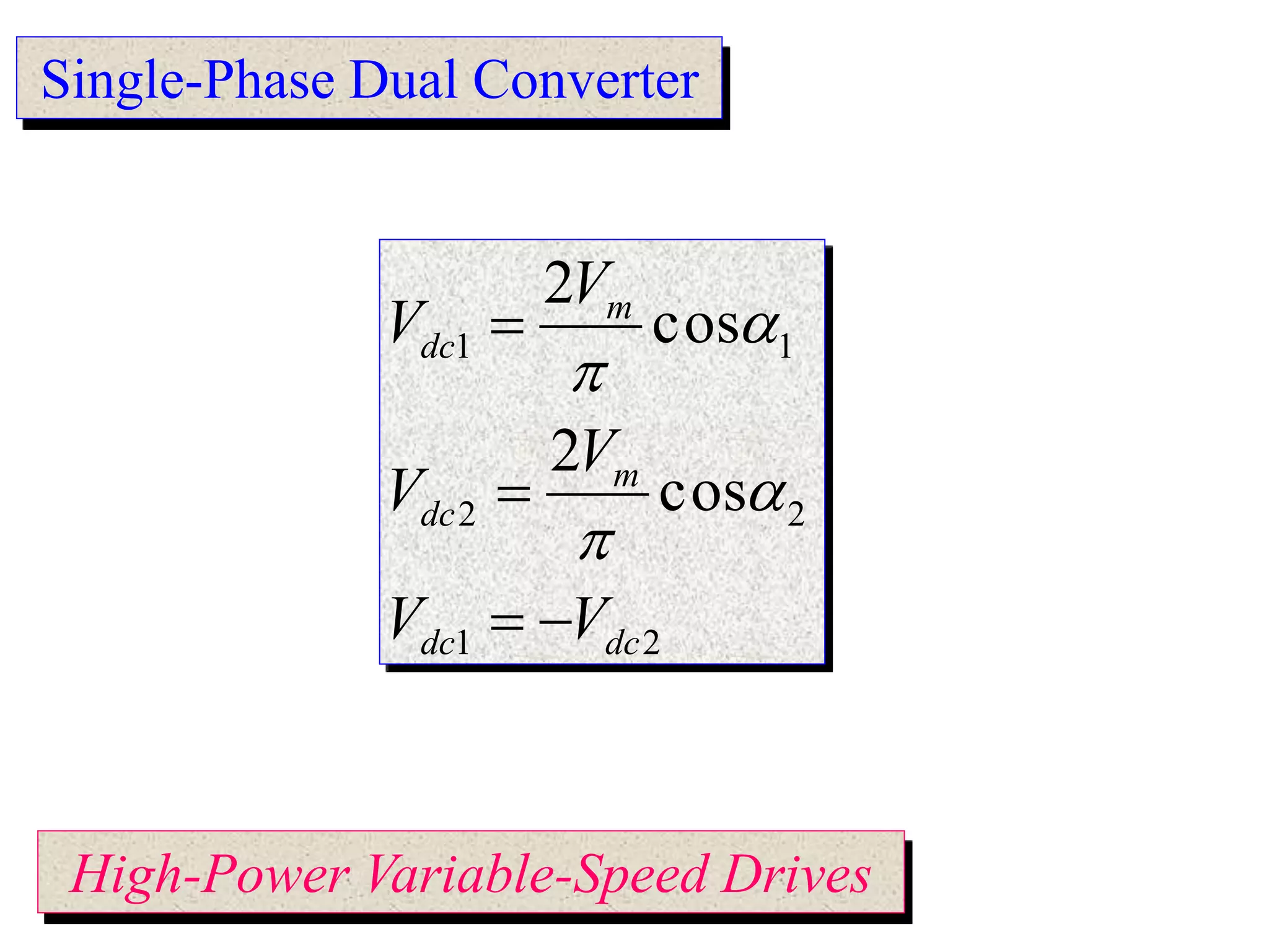


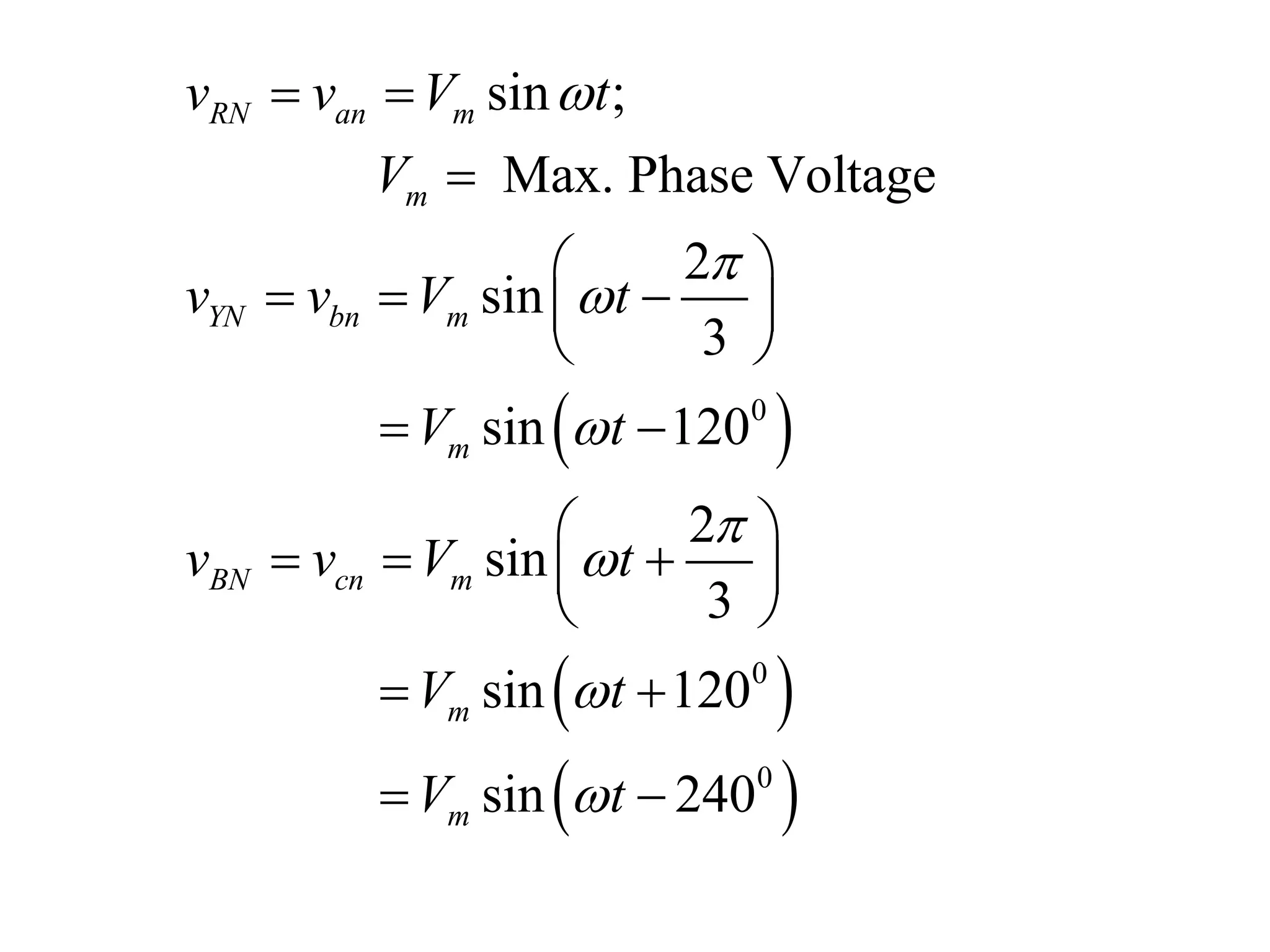
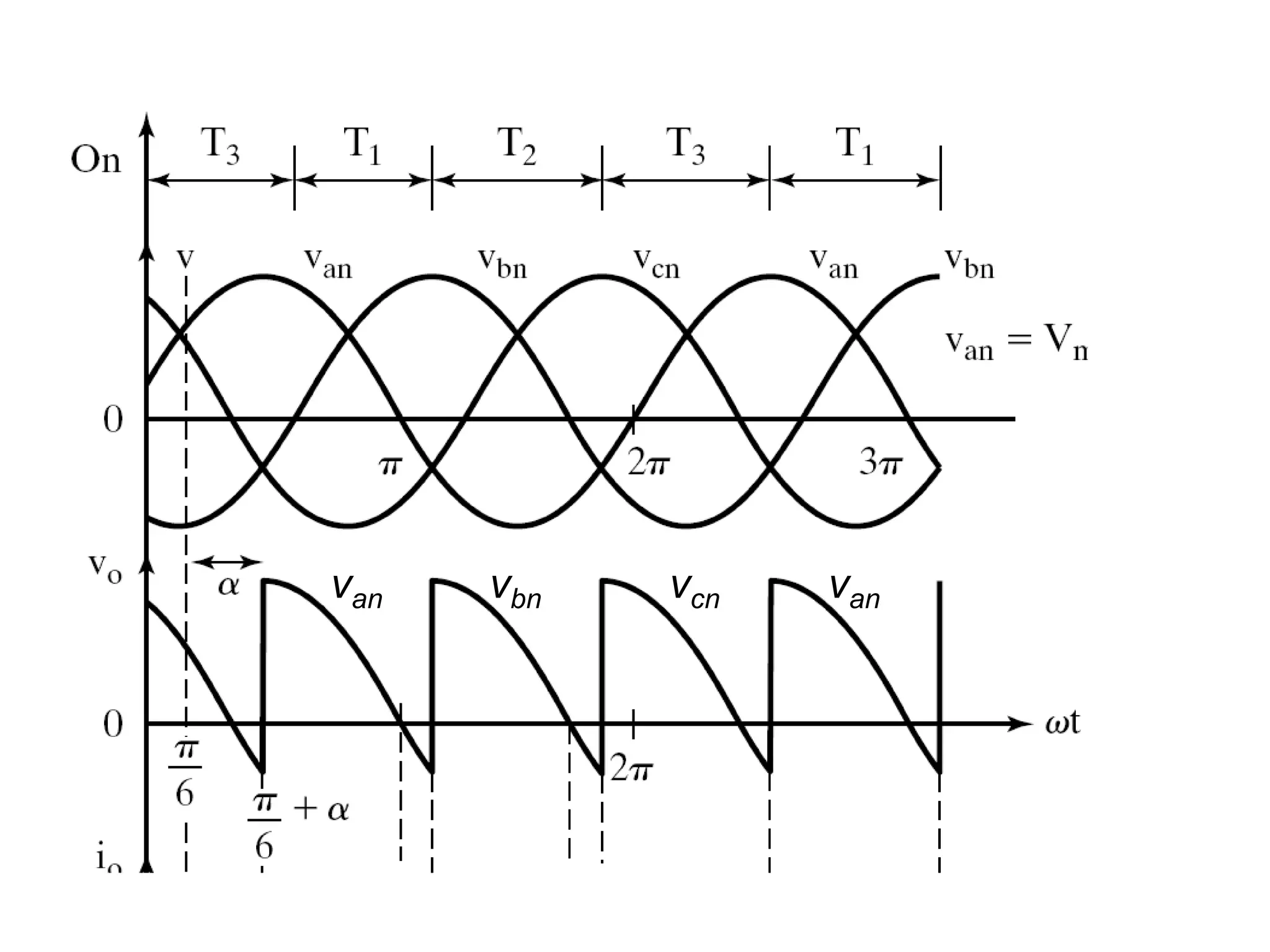


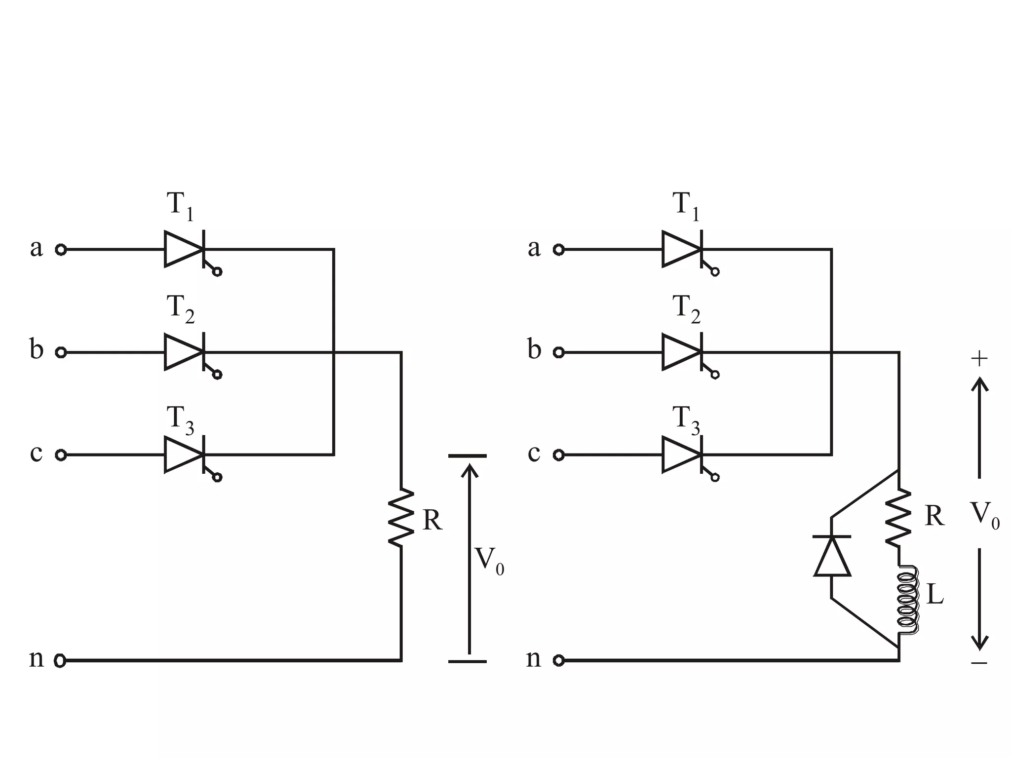

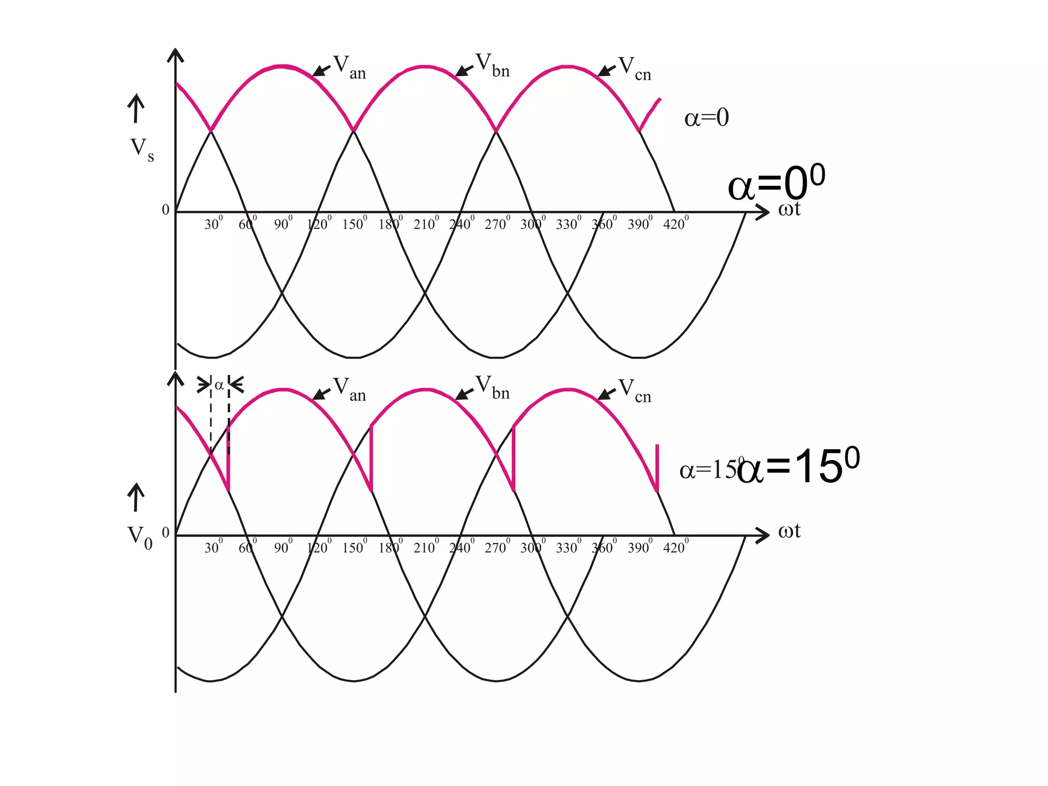
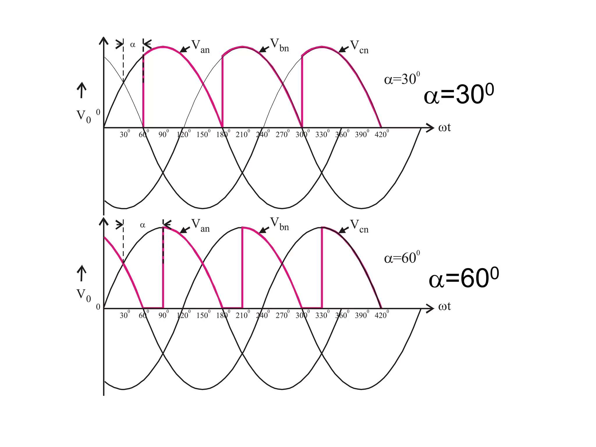


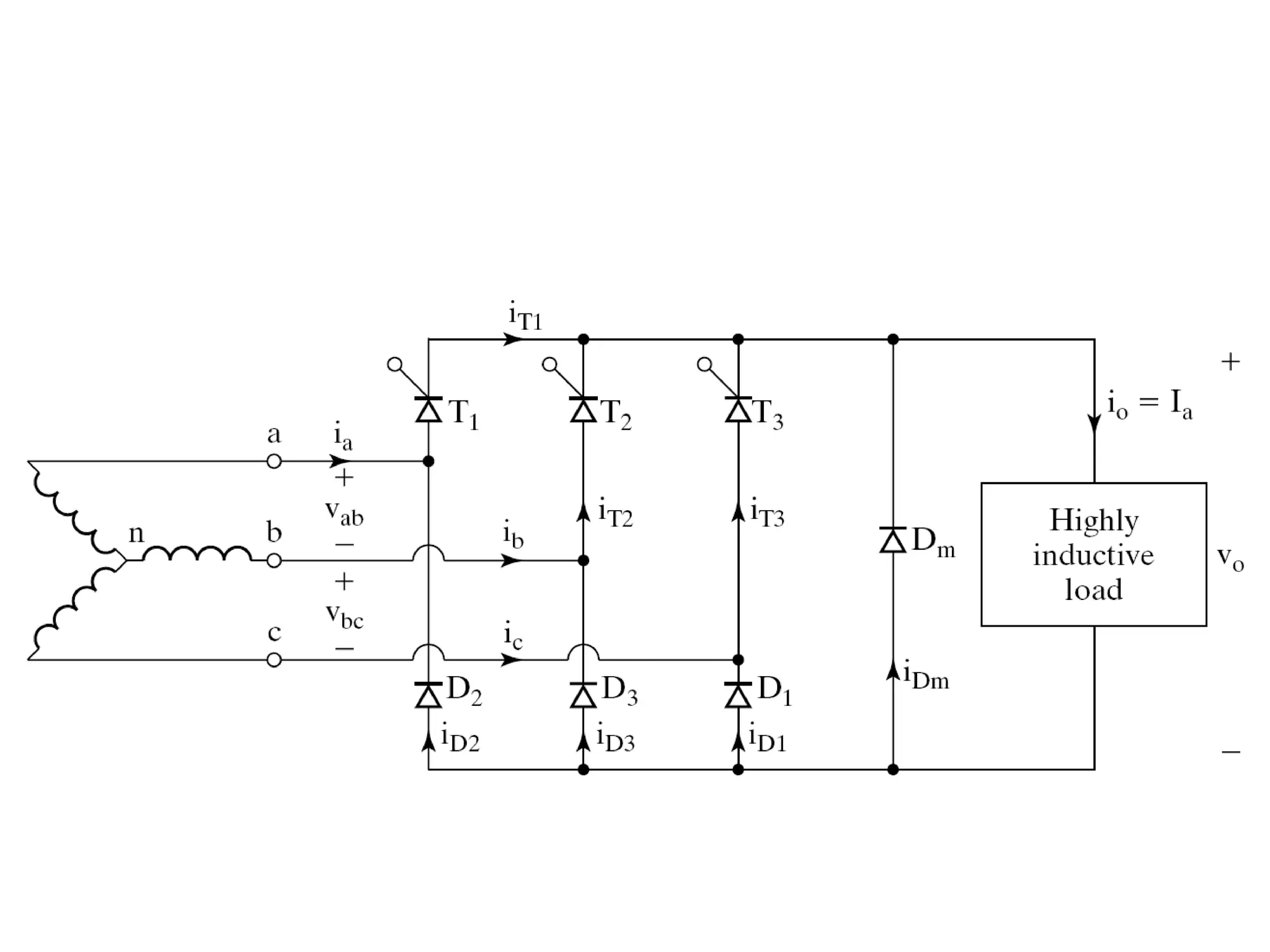
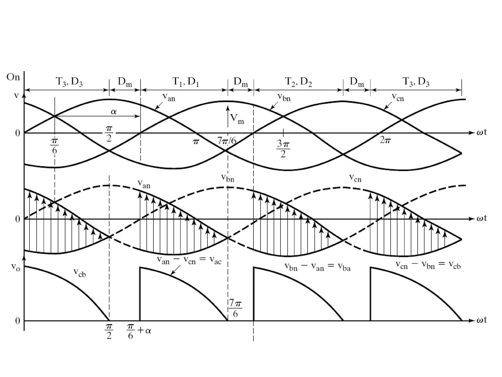


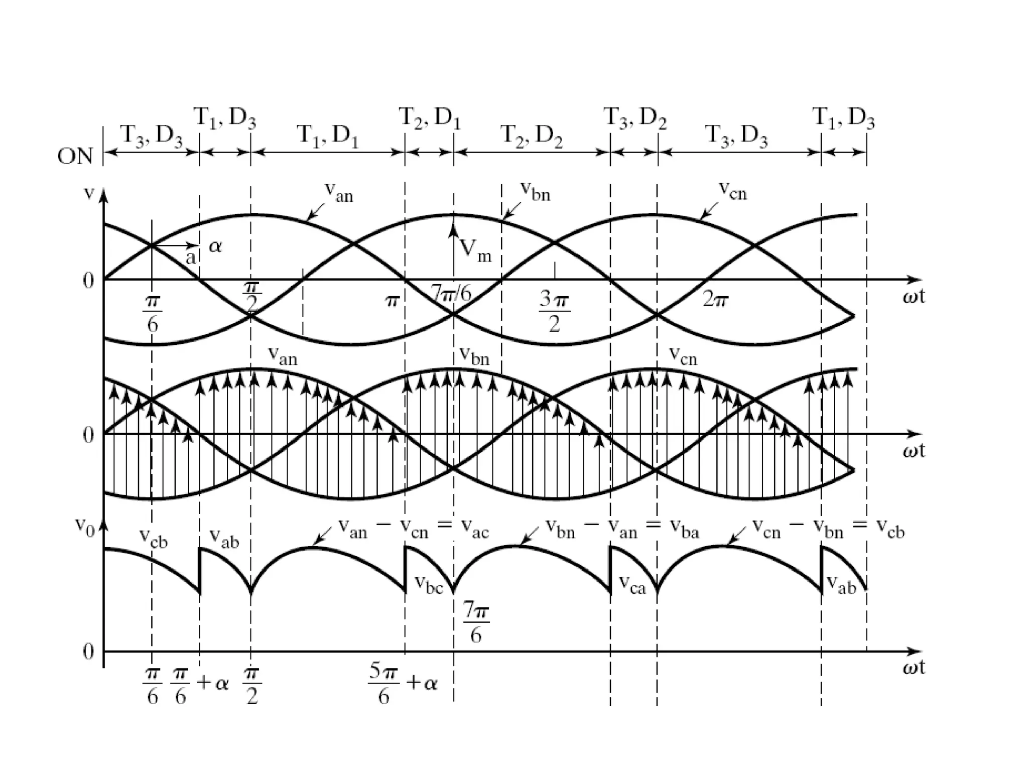
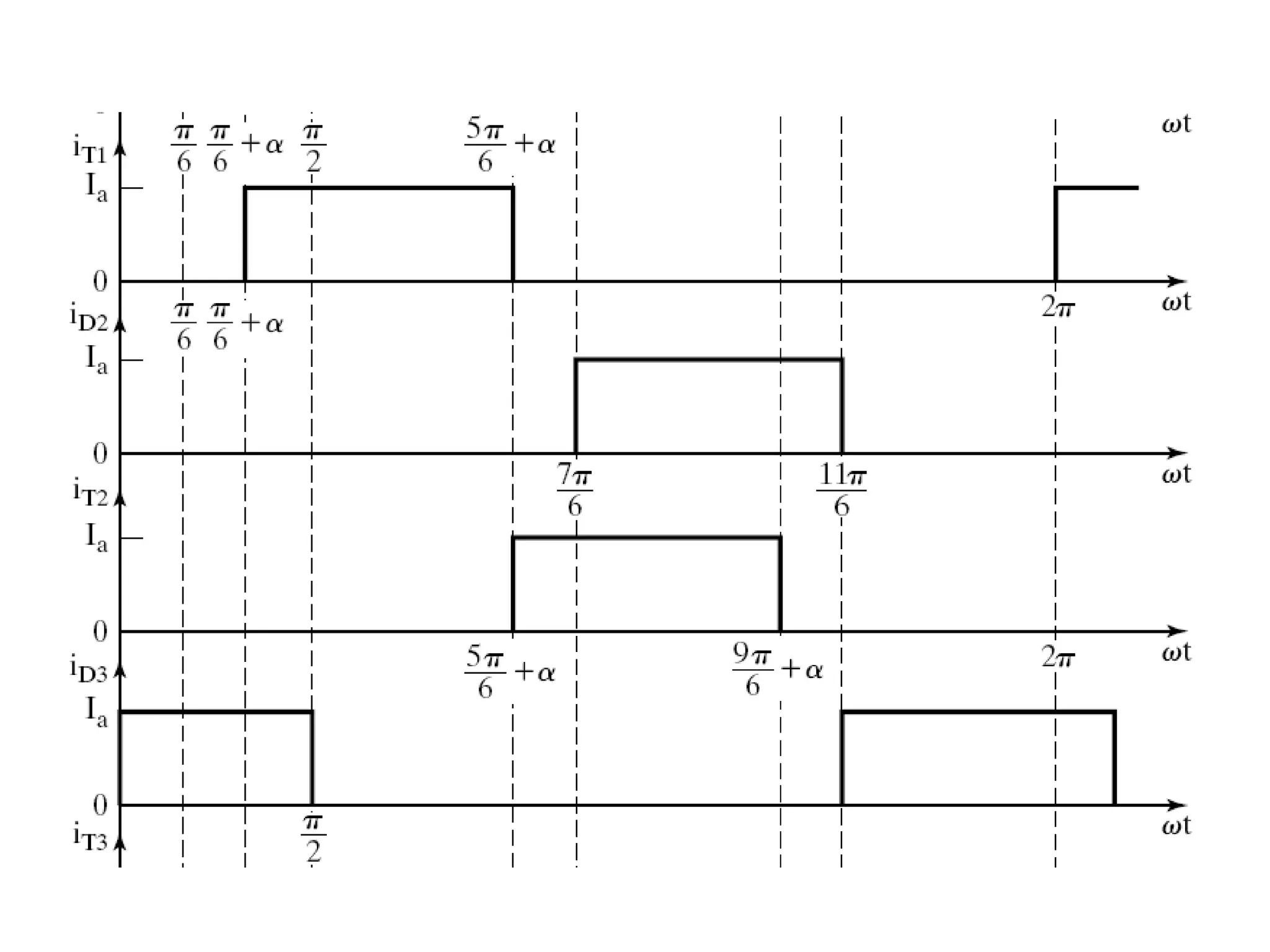
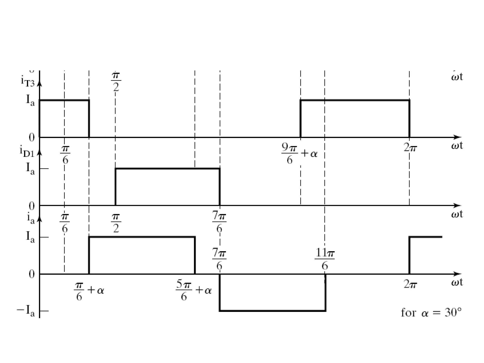

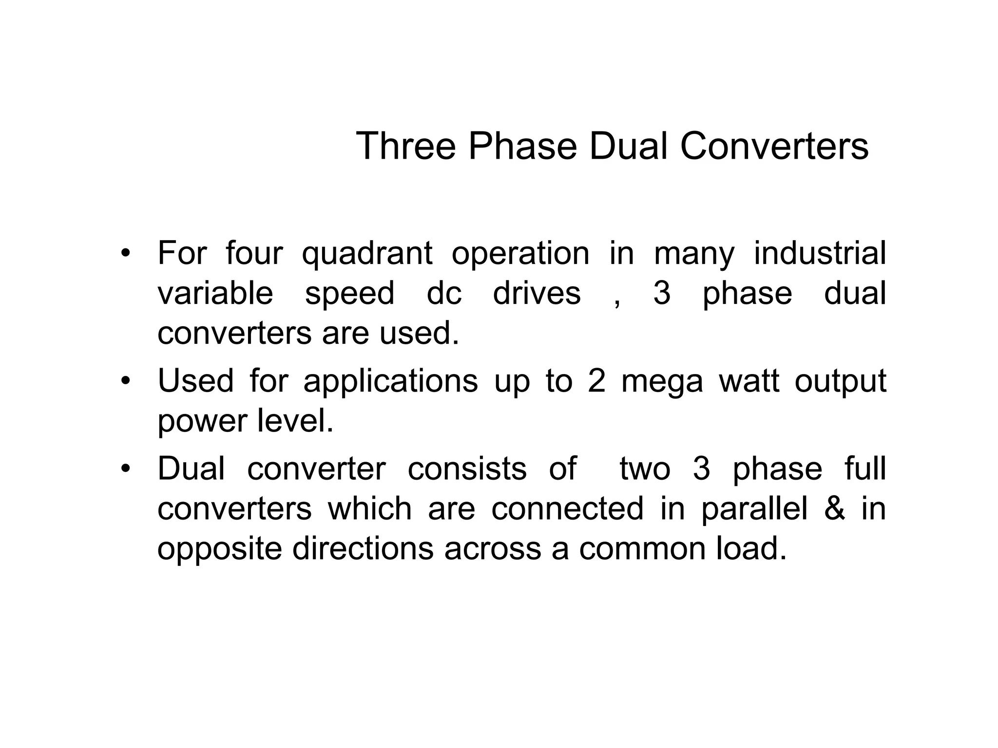


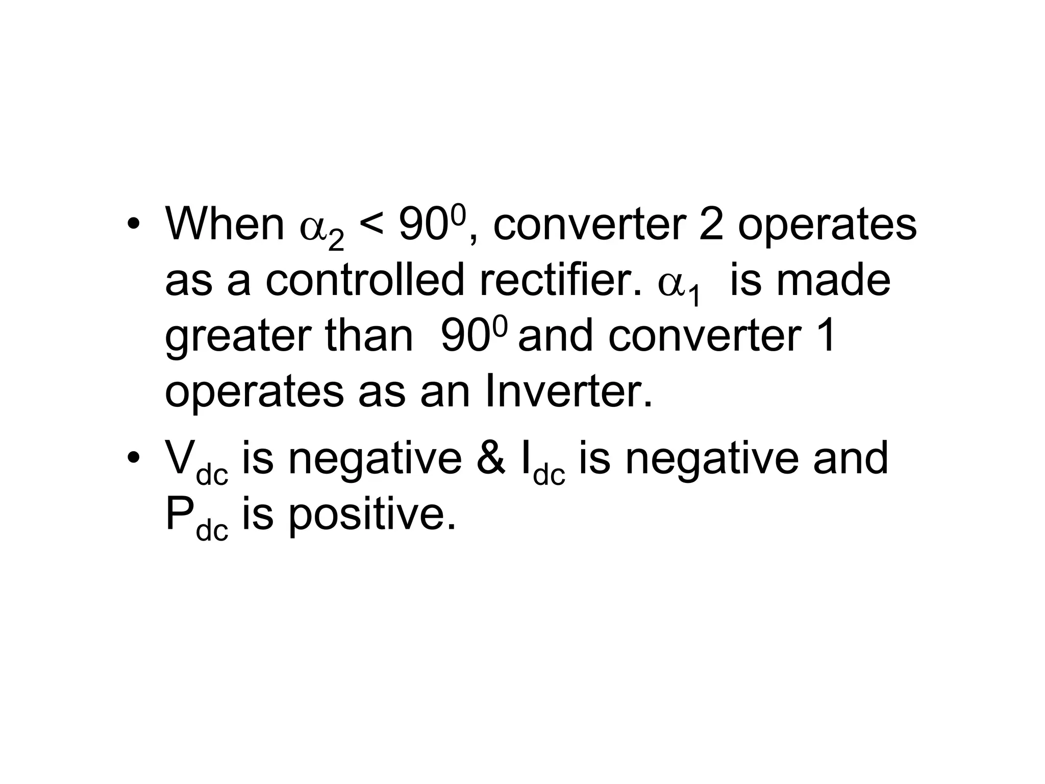

This document discusses various types of phase controlled converters including single-phase and three-phase semiconverters, full converters, and dual converters. It provides equations for the average and RMS output voltage of single-phase converters with resistive and RL loads. It also derives an expression for the average output voltage of a three-phase half wave converter with continuous and constant load current. Key aspects of three-phase half wave, full wave, and dual converters are summarized.


