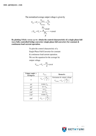
1) The document discusses line-commutated AC to DC converters and phase-controlled rectifiers. Phase-controlled rectifiers can control the DC output voltage by varying the trigger angle, unlike uncontrolled diode rectifiers which provide a fixed output.
2) Applications of phase-controlled rectifiers include DC motor control, AC traction systems, electrochemical processes, and portable tool drives.
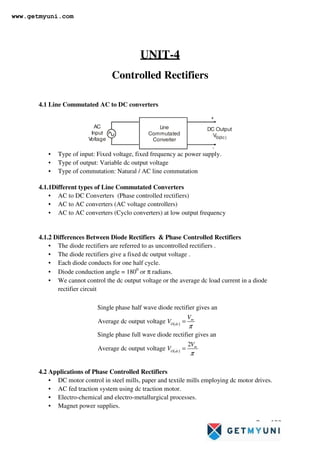
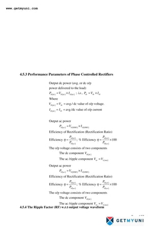
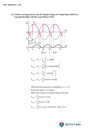
3) Key principles of phase-controlled rectifier operation are derived, including expressions for average DC output voltage and RMS output voltage of a single phase half-wave thyristor converter.

![Page 132
Equations:
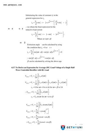
4.4.1 To Derive an Expression for the Average (DC) Output Voltage across the Load
sin i/p ac supply voltage
max. value of i/p ac supply voltage
RMS value of i/p ac supply voltage
2
output voltage across the load
s m
m
m
S
O L
v V t
V
V
V
v v
ω
= =
=
= =
= =
When the thyristor is triggered at
sin ; to
Load current; to
sin
sin ; to
Where max. value of load current
O L m
O
O L
m
O L m
m
m
t
v v V t t
v
i i t
R
V t
i i I t t
R
V
I
R
ω α
ω ω α π
ω α π
ω
ω ω α π
=
= = =
= = = =
= = = =
= =
( ) ( )
( ) ( )
( ) ( )
2
0
1
. ;
2
sin
1
sin .
2
1
sin .
2
dc O
O dc
O m
dc m
O dc
m
O dc
V V v d t
v V t for t to
V V V t d t
V V t d t
π
π
α
π
α
ω
π
ω ω α π
ω ω
π
ω ω
π
= =
= =
= =
=
∫
∫
∫
( ) ( )
( )
( ) [ ]
( ) [ ]
sin .
2
cos
2
cos cos ; cos 1
2
1 cos ; 2
2
m
O dc
m
O dc
m
O dc
m
m S
O dc
V
V t d t
V
V t
V
V
V
V V V
π
α
π
α
ω ω
π
ω
π
π α π
π
α
π
=
= −
= − + = −
= + =
∫
www.getmyuni.com](https://image.slidesharecdn.com/electrical-engineeringengineeringpower-electronicscontrolled-rectifiersnotes-230120172126-0b4249aa/85/electrical-engineering_engineering_power-electronics_controlled-rectifiers_notes-pdf-3-320.jpg)
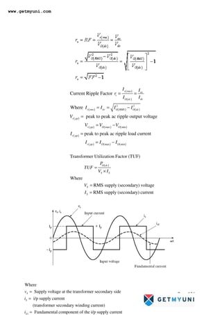
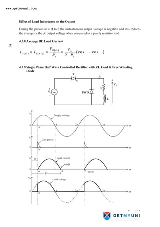
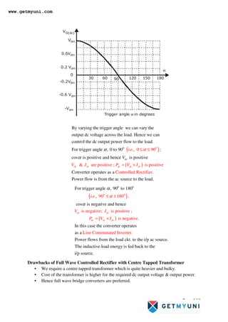
![Page 133
4.5 Control Characteristic of Single Phase Half Wave Phase Controlled Rectifier with
Resistive Load
4.5.1 Control Characteristic
( ) ( ) ( )
( )
max
max
Maximum average (dc) o/p
voltage is obtained when 0
and the maximum dc output voltage
1 cos0 ; cos 0 1
2
m
dm
dc
m
dm
dc
V
V V
V
V V
α
π
π
=
= = + =
∴ = =
( ) [ ]
( )
( )
( )
0
1 cos ; 2
2
The average dc output voltage can be varied
by varying the trigger angle from 0 to a
maximum of 180 radians
We can plot the control characteristic
v by using the eq
m
m S
O dc
O dc
V
V V V
V s
α
π
α
π
α
= + =
( )
uation for O dc
V
( ) [ ]
The average dc output voltage is given by the
expression
1 cos
2
We can obtain the control characteristic by
plotting the expression for the dc output
voltage as a function of trigger angle
m
O dc
V
V α
π
α
= +
www.getmyuni.com](https://image.slidesharecdn.com/electrical-engineeringengineeringpower-electronicscontrolled-rectifiersnotes-230120172126-0b4249aa/85/electrical-engineering_engineering_power-electronics_controlled-rectifiers_notes-pdf-4-320.jpg)
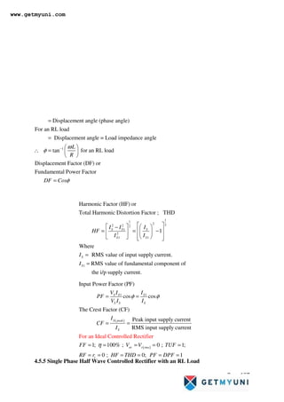

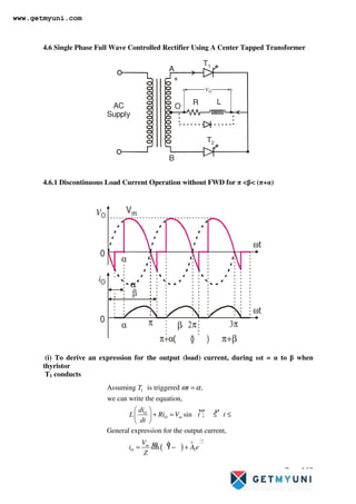
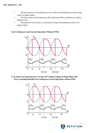
![Page 142
For Large Load Inductance the load current does not reach zero, & we obtain
continuous load current.
2π 3π
π
α
0 ωt
2π+α
t1
i0
SCR SCR
FWD FWD
t3
t2 t4
[ ]
The followi
The average
ng points a
output voltage
1 cos which is the same as that
2
of a purely resistive load.
For low value of inductance, the load current
tends to become dis
re to be noted
cont
m
dc
V
V α
π
= +
inuous.
During the period to
the load current is carried by the SCR.
During the period to load current is
carried by the free wheeling diode.
The value of depends on the value of
R and L and the forwa
α π
π β
β
rd resistance
of the FWD.
www.getmyuni.com](https://image.slidesharecdn.com/electrical-engineeringengineeringpower-electronicscontrolled-rectifiersnotes-230120172126-0b4249aa/85/electrical-engineering_engineering_power-electronics_controlled-rectifiers_notes-pdf-13-320.jpg)
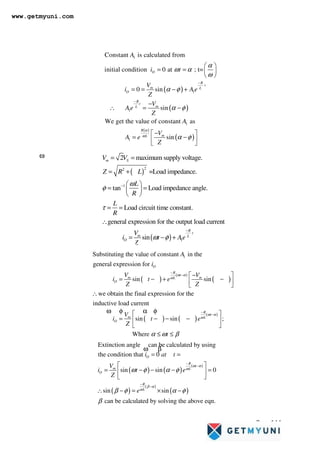
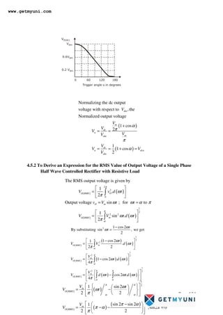
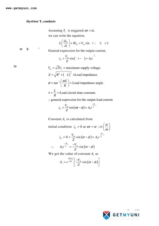
![Page 146
(iii) To calculate the RMS output voltage we use the expression
(iv) Discontinuous Load Current Operation with FWD
vO
Vm
0
α
2π 3π
α π β
( )
π+α ( )
π+β
α
β
iO
ωt
ωt
0
(v) To Derive an Expression for the DC Output Voltage for a Single Phase Full
Wave Controlled Rectifier with RL Load & FWD
( )
( )
2
2
1
1
Thyristor is trigger
Thyristor is triggered at ;
conducts from to
FWD conducts from to &
0 during discontinuous loa
ed at ;
conducts from t
d current.
o 2
O
T t
T
T t
t
T t
t
v
ω π α
ω
ω α
ω
π
ω π β
α
α π
π
= +
=
=
≈
= +
=
( ) ( )
( ) ( )
( )
( ) [ ]
( ) ( )
0
1
.
1
sin .
cos
cos cos ; cos 1
1 cos
dc O
O dc
t
dc m
O dc
m
dc
O dc
m
dc
O dc
m
dc
O dc
V V v d t
V V V t d t
V
V V t
V
V V
V
V V
π
ω
π
α
π
α
ω
π
ω ω
π
ω
π
π α π
π
α
π
=
= =
∴ = =
= = −
= = − + = −
∴ = = +
∫
∫
www.getmyuni.com](https://image.slidesharecdn.com/electrical-engineeringengineeringpower-electronicscontrolled-rectifiersnotes-230120172126-0b4249aa/85/electrical-engineering_engineering_power-electronics_controlled-rectifiers_notes-pdf-17-320.jpg)
![Page 148
• By plotting VO(dc) versus α, we obtain the control characteristic of a single phase
full wave controlled rectifier with RL load for continuous load current operation
without FWD
( ) ( )
( )
( ) ( )
( )
( )
( )
1
.
1
sin .
cos
dc O
O dc
t
dc m
O dc
m
dc
O dc
V V v d t
V V V t d t
V
V V t
π α
ω α
π α
α
π α
α
ω
π
ω ω
π
ω
π
+
=
+
+
= =
= =
= = −
∫
∫
( )
( )
( )
( ) [ ]
( )
cos cos ;
cos cos
cos cos
2
cos
dc
O dc
m
m
dc
O dc
m
dc
O dc
V V
V
V
V V
V
V V
α π α
π
π α α
α α
π
α
π
=
= − +
+ = −
= = +
∴ = =
c o s
d c d m
V V α
= ×
www.getmyuni.com](https://image.slidesharecdn.com/electrical-engineeringengineeringpower-electronicscontrolled-rectifiersnotes-230120172126-0b4249aa/85/electrical-engineering_engineering_power-electronics_controlled-rectifiers_notes-pdf-19-320.jpg)
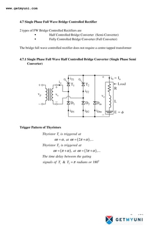
![Page 152
Thyristor T1 and D1 conduct from ωt = α to π
Thyristor T2 and D2 conduct from ωt = (π + α) to 2 π
FWD conducts during ωt = 0 to α, π to (π + α) , …..
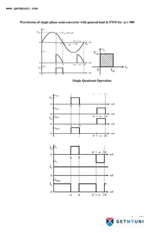
Load Voltage Load Current Waveform of Single Phase Semi Converter for α
α
α
α 900
Continuous load current operation
vO
Vm
0
α
iO
ωt
2π 3π
α π
( )
π+α
α
ωt
0
α α
( )
2π+α
(i) To Derive an Expression for The DC Output Voltage of A Single Phase Semi
Converter with R, L, E Load FWD For Continuous, Ripple Free Load Current
Operation
( ) ( )
( ) ( )
( )
( ) [ ]
( ) ( )
0
1
.
1
sin .
cos
cos cos ; cos 1
1 cos
dc O
O dc
t
dc m
O dc
m
dc
O dc
m
dc
O dc
m
dc
O dc
V V v d t
V V V t d t
V
V V t
V
V V
V
V V
π
ω
π
α
π
α
ω
π
ω ω
π
ω
π
π α π
π
α
π
=
= =
∴ = =
= = −
= = − + = −
∴ = = +
∫
∫
www.getmyuni.com](https://image.slidesharecdn.com/electrical-engineeringengineeringpower-electronicscontrolled-rectifiersnotes-230120172126-0b4249aa/85/electrical-engineering_engineering_power-electronics_controlled-rectifiers_notes-pdf-23-320.jpg)
![Page 155
iO
Constant Load Current
i =I
O a
α π+α
α π+α 2π+α
i
i
T1
T2
Ia
π+α 2π+α 3π+α
ωt
ωt
ωt
Ia
i
i
T3
T4
Ia
Ia
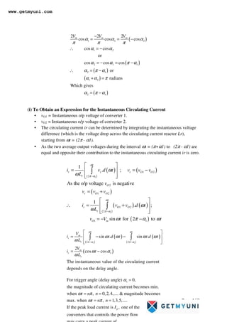
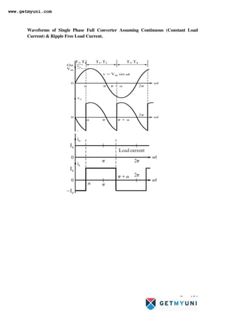
(i) To Derive An Expression For The Average DC Output Voltage of a Single Phase Full
Converter assuming Continuous Constant Load Current
( ) ( )
2
0
The average dc output voltage
can be determined by using the expression
1
. ;
2
The o/p voltage waveform consists of two o/p
pulses during the input supply time period of
0 to 2 r
dc O
O dc
V V v d t
π
ω
π
π
= =
∫
adians. Hence the Average or dc
o/p voltage can be calculated as
( ) ( )
( ) [ ]
( )
2
sin .
2
2
cos
2
2
cos
dc m
O dc
m
dc
O dc
m
dc
O dc
V V V t d t
V
V V t
V
V V
π α
α
π α
α
ω ω
π
ω
π
α
π
+
+
= =
= = −
= =
∫
( ) ( )
( )
0
max
max
Maximum average dc output voltage is
calculated for a trigger angle 0
and is obtained as
2 2
cos 0
2
m m
dm
dc
m
dm
dc
V V
V V
V
V V
α
π π
π
=
= = × =
∴ = =
www.getmyuni.com](https://image.slidesharecdn.com/electrical-engineeringengineeringpower-electronicscontrolled-rectifiersnotes-230120172126-0b4249aa/85/electrical-engineering_engineering_power-electronics_controlled-rectifiers_notes-pdf-26-320.jpg)